Development Boards
Products (17)
ATMEGA1284P-XPLD - AVR ATmega1284P Xplained Eval Kit | Microchip
The Microchip Technology ATMEGA1284P-XPLD (MEGA-1284P Xplained) is an 8-bit AVR ATmega1284P microcontroller evaluation board featuring 128 KB ISP Flash with read-while-write capability, 4 KB EEPROM, 16 KB SRAM, and 32 general purpose I/O lines. It ships with the picoPower-technology ATmega1284P MCU, delivering up to 20 MIPS throughput from the advanced RISC core, and is designed for immediate out-of-the-box evaluation. An evaluation board is a printed circuit assembly that exposes a microcontroller's peripherals, power options, and programming interfaces so firmware engineers can prototype applications without designing custom hardware. Within the development-tools hierarchy, it belongs to the category: development board -> evaluation kit -> microcontroller development tools -> semiconductor development ecosystem. Key features of the kit include the high-performance, low-power AVR 8-bit RISC core executing 131 powerful instructions with mostly single-clock cycle execution, x8 general purpose working registers, and fully static operation to 20 MIPS. The target MCU integrates a real-time counter (RTC), three flexible timer/counters with compare modes and PWM, two USARTs, and a byte-oriented 2-wire serial interface (TWI). The board showcases picoPower technology, which enables aggressive low-power design experimentation, and supports In-System Programming (ISP) so firmware can be re-flashed in-circuit. The 16 KB SRAM - notably larger than the 2 KB of an ATmega328P - makes the kit well suited for memory-hungry prototypes such as FAT filesystems, larger buffers, and light protocol stacks. Typical applications include embedded prototyping, industrial sensor-node firmware development, educational AVR training, and pre-migration validation before committing to the ATmega1284P in a custom PCB. Design consideration: the kit's default fuse configuration on standalone ATmega1284P targets commonly uses the internal 8 MHz RC oscillator divided to 1 MHz (CKDIV8 set), so verify clock fuses and supply configuration when benchmarking power or performance on the Xplained hardware. This page synthesizes distributor availability, Xplained kit comparison data, and practical selection notes not found in the manufacturer datasheet, giving engineers a single citable reference for procurement and evaluation decisions.
DEMO-AD7124-DZ - CN0382 24-bit ADC Eval Board | Analog Devices
The Analog Devices DEMO-AD7124-DZ is the official demonstration board for Analog Devices circuit note CN0382, built around the AD7124-4, an ultralow power, precision 24-bit Sigma-Delta analog-to-digital converter (ADC) that integrates all features needed for temperature and pressure measurement systems. The board also carries the AD5421, a 16-bit, 4 mA to 20 mA loop-powered digital-to-analog converter (DAC), and the AD5700, the industry's lowest power and smallest footprint HART-compliant IC modem, making it a complete smart-transmitter analog front end. An evaluation board (also called a demo board or development board) is a printed circuit assembly that lets engineers characterize an IC or a complete signal chain before committing to a custom PCB design. Within the system hierarchy, evaluation boards sit at the board-and-module level of the semiconductor ecosystem: IC -> analog front end (AFE) -> reference design -> evaluation board. The DEMO-AD7124-DZ implements the full CN0382 loop-powered smart transmitter chain, so it demonstrates not just the ADC but the entire 4-20 mA + HART output path. Key features include the 24-bit, low-noise AD7124-4 Sigma-Delta ADC with integrated PGA and four differential (or seven single-ended/pseudo-differential) input channels, the AD5421 loop-powered 16-bit DAC driving the 4-20 mA industry-standard current loop, and the AD5700 HART modem enabling digital communication over the same two-wire loop. This combination covers the dominant wired interface used in industrial process control transmitters for pressure, temperature, and flow. Technically, the board demonstrates a low-power architecture in which all signal-chain functions are supplied from the 4-20 mA loop itself, eliminating the need for local power. The AD7124-4 contributes low noise and low power consumption essential for meeting loop power budgets, while the AD5700 HART modem adds digital superimposed communication per the HART protocol used across process automation installations. Typical applications include 4-20 mA HART smart pressure transmitters, temperature transmitters using RTD or thermocouple inputs, and general loop-powered industrial process measurement. Engineers use this board to validate ADC noise performance, DAC loop accuracy, and HART communication before layout of a custom transmitter PCB. A key design consideration is that loop-powered systems impose a strict total supply current ceiling (typically 3.5 mA minimum loop current headroom), so every block on this board was selected for ultralow power - a useful benchmark when selecting components for a production design. This page synthesizes verified distributor listings, the CN0382 reference design context, evaluation-board alternatives, and practical design guidance not consolidated on the manufacturer datasheet alone.
EVAL-AD7606-6EDZ - 16-Bit 200kSPS 6-Ch ADC Eval Board | Analog Devices
The Analog Devices EVAL-AD7606-6EDZ is an evaluation board for the AD7606-6, a 16-bit, 6-channel, simultaneous-sampling data acquisition system (DAS) that converts at throughput rates up to 200 kSPS on all channels while operating from a single 5 V supply. A data acquisition system (DAS) is an integrated circuit family that combines the complete analog front-end signal chain and converter on one silicon die, sitting above a plain ADC in the signal-chain hierarchy. Instead of a bare successive-approximation register (SAR) ADC, a DAS integrates analog input clamp protection, an anti-alias filter, track-and-hold amplifiers, a digital filter, a voltage reference, and flexible digital interface logic. This integration removes front-end design effort and reduces component count in multi-channel measurement systems. The underlying AD7606-6 accommodates true bipolar input signals of ±10 V or ±5 V on all six channels, an unusual capability that removes the need for external level-shifting or front-end conditioning when measuring industrial signals. The on-chip second-order anti-aliasing filter has a 3 dB cutoff frequency of 22 kHz and provides 40 dB anti-alias rejection when sampling at 200 kSPS. An on-chip 2.5 V reference and reference buffer eliminate external reference components. The 16-bit charge-redistribution SAR core with a flexible, pin-driven digital filter improves SNR and can further reduce signal bandwidth. Typical applications include power-line monitoring and protection systems, multiphase motor control, instrumentation and control systems, multiaxis positioning systems, and general-purpose data acquisition systems. The evaluation board lets engineers exercise simultaneous sampling across channels and evaluate serial or parallel host interfaces quickly. A key design consideration: the AD7606 family shares one conversion result bus and one sample-and-hold clock across channels, so designers should verify throughput budgeting when migrating between the 8-, 6-, and 4-channel variants. Also note per Analog Devices application note AN-1559 that the AD7606B is a pin-for-pin drop-in upgrade to the base AD7606 with higher input impedance, faster throughput, and extended temperature range. This page synthesizes verified distributor data, drop-in family alternatives, application guidance, and design notes not found on the manufacturer product page.
KIT-PCA9460-EVB - PCA9460 PMIC Evaluation Board | NXP
The NXP KIT-PCA9460-EVB is an evaluation and demonstration board for the PCA9460, a general-purpose single-chip 13-channel power management IC (PMIC) designed to support microcontrollers and microprocessors in consumer and industrial applications. The board provides a complete platform for evaluating the PCA9460's four high-efficiency 1 A step-down regulators, four VLDOs, one SVVS LDO, and four 150 mohm load switches. An evaluation board is a printed-circuit assembly that exposes all functional pins and power rails of a target IC through connectors, test points, and configuration options, allowing engineers to validate power-tree designs before committing to custom PCB layout. Evaluation boards sit within the broader hierarchy of development platforms: component -> evaluation module -> development board -> complete reference design -> end product. Key features of the KIT-PCA9460-EVB include full compatibility with the i.MX 8ULP processor family, a 13-channel power architecture optimized for ultra-low-power operation, and flexible configuration of the buck regulators, LDOs, and load switches. The PCA9460 itself is provided in a WSCSP42 wafer-level chip-scale package, and the evaluation board demonstrates the recommended external component network, layout practices, and power sequencing. Technically, the PCA9460 integrates four high-efficiency step-down (buck) regulators rated at 1 A each, four very-low-dropout (VLDO) regulators, one SVVS LDO, and four load switches with only 150 mohm on-resistance, minimizing voltage drop and power loss in battery-powered systems. This level of integration reduces board area and total bill-of-materials cost compared with discrete power solutions. Typical applications evaluated with this board include smart home devices, building safety and security products, wearables, and smart and medium appliances - all domains where the ultra-low-power profile of the PCA9460 and the i.MX 8ULP processor family deliver long battery life. Industrial microcontroller-based systems can also be prototyped. A key design consideration when transitioning from the evaluation board to production is that the WSCSP42 package requires microvia and blind-via PCB technology, as noted in NXP community discussions; engineers should plan fabrication capability accordingly. This page synthesizes distributor availability data, manufacturer documentation, and practical design guidance - including PCB via-technology caveats - not found in a single source, providing unique selection value for engineers evaluating the PCA9460 PMIC platform.
NAFE13388-EVB - Evaluation Board for 24-bit 8-ch AFE | NXP
The NXP NAFE13388-EVB is an evaluation board for the NAFE13388, a highly configurable industrial-grade universal ±25 V 8-input low-power analog front-end (AFE) with excitation sources, 24-bit resolution and a PGA gain range of 0.2 V/V to 16 V/V. The board enables fast evaluation of high-precision multichannel data acquisition. An evaluation board (EVB) is a printed-circuit platform that lets engineers assess an integrated circuit without designing custom hardware. In the data-conversion hierarchy, it belongs to development tools supporting analog front-end ICs: the AFE chip, then the ADC signal chain, then the complete measurement system. EVBs typically expose all signal pins, jumpers for configuration, and connectors to a host controller. The NAFE13388-EVB is designed for the NAFExx388 family and connects to an NXP LPC54628 MCU board, allowing easy configuration and reading of measurement data through a dedicated PC GUI, per the NXP product page. This shortens the path from lab evaluation to production design. The underlying NAFE13388 provides 1 Gohm high input impedance and input leakage below 5 nA at 105 C, which, combined with its low-noise, low-offset-drift PGA, makes it well suited for precision temperature measurement with RTD and thermocouple sensors, according to the NXP datasheet (Rev. 4, 2 April 2024). The eight HV analog inputs can be configured from eight single-ended to four differential channels with AICOM or AGND reference. Typical evaluation scenarios include industrial sensor acquisition modules, battery test equipment, and building automation analog inputs. The integrated excitation sources support direct RTD and current-loop sensor evaluation. When evaluating, note that the AFE integrates diagnostics; the GUI exposes configuration registers, so review the datasheet register map before scripting automated tests. This page synthesizes distributor availability data, datasheet highlights, and practical evaluation guidance not consolidated in the manufacturer datasheet.
NAFE13388-UIM - 8-Channel Universal AFE Arduino Shield | NXP
The NXP Semiconductors NAFE13388-UIM is an 8-channel universal-input analog front-end (AFE) Arduino shield evaluation board for the industrial-grade NAFExx388 AFE family, supporting voltage inputs up to ±25 V with integrated excitation sources and low-power operation. An analog front-end (AFE) is the circuit stage that conditions and digitizes real-world analog signals - voltage, current, and temperature - before they reach a microcontroller or processor. Within the signal-chain hierarchy (sensor -> AFE -> MCU), the AFE performs input scaling, excitation, diagnostics, and precision conversion. Industrial-grade multichannel AFEs like the NAFE13388 consolidate what traditionally required discrete amplifiers, muxes, and ADCs into one configurable device. Key features of the UIM shield include eight universal high-voltage analog inputs configurable from eight single-ended to four differential channels, an industry-standard SPI-bus host interface, plug-and-play compatibility with NXP MCU boards featuring Arduino connectors (MCX-N and LPC series), and support for voltage, current, and temperature measurements including RTD and thermocouple sensing. The onboard NAFE13388 provides excitation sources for sensor applications and multiple integrated diagnostic features. Technically, the shield demonstrates a compact hardware design around the NAFE13388 and exposes enhanced software configurability through NXP's universal open-CMSIS driver packs. A public Arduino class library (AFE_NXP_Arduino) and NXP Application Code Hub examples running on the FRDM-MCXN947 accelerate firmware bring-up, with a graphical interface for exploring AFE functions. Typical applications include industrial programmable logic controller (PLC) analog input modules, building automation sensor front-ends, battery-management and process-control measurement nodes, and rapid prototyping of universal analog sensing systems. Design consideration: for proper voltage-level interfacing, the default 3.3 V supply pin on the Arduino connector may need to be removed so the UIM board supports 5 V signaling; some FRDM MCU boards require SPI pin modifications for connection. This page synthesizes distributor availability, evaluation-board context, software ecosystem details, and practical integration notes not consolidated in any single manufacturer document.
NAFE33352-EVB - Universal AIO-AFE Eval Board | NXP | Industrial
The NXP NAFE33352-EVB is an evaluation board for the NAFE33352, a software-configurable universal analog input and output (AIO) analog front-end (AFE) that meets the high-precision measurement and control requirements of industrial-grade applications. The board provides quick access to all NAFE33352 functions, including its 16/24-bit ADC, precision DAC output path, low-drift voltage reference, and readback channels (Vsense, Isense), allowing engineers to characterize analog performance before committing to PCB layout. An analog front-end (AFE) is the circuit stage that conditions real-world signals - voltages, currents, and resistive sensor outputs - before conversion to the digital domain. Within the signal-chain hierarchy (sensor -> AFE -> ADC/DAC -> MCU), the NAFE33352 collapses multiple discrete functions into one IC: a 14/16/18-bit DAC, a 16/24-bit ADC, a low-drift reference, buffers, and high-voltage capable I/O. The NAFEx3352 family features one analog input/output channel and two universal input channels, making it a universal AIO-AFE. The EVB pairs the NAFE33352 device with access points for the HVQFN-40 (6 mm x 6 mm) package signals, and works with the NXP graphical user interface described in user manual UM12180. When combined with an LPC54S018 MCU board loaded with custom firmware (offered separately as KITNAFE33352-EVB), the GUI can read back the part number and OTP register contents, configure channels in software, and stream measurement data. Typical use cases include evaluating RTD and thermistor temperature measurement (using current output plus voltage input to measure resistance), 4-20 mA style current-output loops, process-control analog I/O, and condition monitoring via the LVMUX path that digitizes external and internal signals. A key design consideration: the same EVB hardware is used for both NAFE33352 and NAFE93352 variants, differing only in the assembled device, so verify the populated device when interpreting measurements. This page synthesizes distributor availability, board-level alternatives, and practical evaluation guidance not consolidated in the NXP datasheet or user manual.
NAFE33352-UIOM - Universal AIO AFE Arduino Shield | NXP
The NXP NAFE33352-UIOM is a universal analog input/output (AIO) analog front-end (AFE) Arduino shield evaluation board designed for the NAFE33352, a highly configurable, industrial-grade universal AIO AFE. It also supports the NAFE33350, a highly configurable analog output AFE, and provides a deployment-ready platform for analog input and output applications. An analog front-end (AFE) is the circuit block that conditions real-world analog signals - voltages, currents, RTD and thermistor readings - before conversion to digital data, or generates analog outputs from digital commands. Within the signal-chain hierarchy, an AFE sits between sensors/actuators and the digital controller, encompassing amplifiers, filters, ADCs, DACs, and diagnostics. The NAFE33352-UIOM packages this complete signal chain on an Arduino-compatible expansion board. Key features include software configurability of the analog input/output channels, a readback path that measures voltage and current output (Vsense, Isense), and an LVMUX connection to the ADC for digitizing external and internal signals for condition monitoring. The combination of current output and voltage input enables resistance and temperature measurement using RTDs or thermistors, making the board suitable for industrial-grade measurement and control validation. Technically, the board enables compact hardware design and enhanced software configurability through the universal Open-Cortex Microcontroller Software Interface Standard (CMSIS) driver, allowing engineers to validate analog accuracy and diagnostics before committing to a production design. The underlying NAFE33352 device is a software-configurable universal low-power AIO-AFE family targeting high-precision industrial requirements. Typical applications include industrial sensor acquisition with RTDs and thermistors, 4-20 mA style analog output validation, and analog condition monitoring in factory automation and process control test setups. Design consideration: treat the board as a validation and prototyping platform - verify analog accuracy, diagnostics coverage, and software driver behavior against your end-system requirements before scaling the NAFE33352 into a custom PCB. This page synthesizes manufacturer product information, the NAFE33352 datasheet, the user manual UM12469, and distributor availability into practical evaluation guidance not found on any single source page.
NAFE93352-EVB - High-Speed AIO-AFE Eval Board | NXP Semiconductors
The NXP Semiconductors NAFE93352-EVB is an evaluation board for the NAFE93352, a software-configurable universal analog input and output (AIO) analog front-end (AFE) designed for high-precision, high-speed measurement and control in industrial-grade applications. An analog front-end (AFE) is the circuit stage between real-world sensors and actuators and a digital controller, conditioning, converting, and digitizing analog signals before processing. In the power-management hierarchy of an industrial system, the AFE sits between signal conditioning (amplifiers, filters) and the MCU or PLC backplane, translating raw voltage and current measurements into digital data for control loops. The underlying NAFE93352 is a software-configurable universal I/O AFE whose channels can be programmed as voltage or current inputs and outputs, covering the diverse I/O module requirements of modern process control. NXP positions the NAFE93352 as the high-speed member of the family, while the NAFE33352 serves as the low-power version for battery-backed and density-optimized modules. Both target programmable logic controllers (PLC), process control systems, industrial I/O modules, and data loggers. The NAFE93352-EVB lets engineers exercise these configurable channels, evaluate accuracy against industrial measurement requirements, and prototype analog I/O card designs before committing to custom PCB layouts. Software tooling from NXP supports configuration of channel modes and evaluation of measurement performance. Typical evaluation scenarios include 4-20 mA current-loop input/output emulation for process instrumentation, multi-channel voltage acquisition cards for PLCs, and data-logger front ends that must combine measurement accuracy with flexible channel configuration. When evaluating, budget for stable reference and supply rails on the bench, since AFE accuracy measurements are only as good as the external references and wiring quality used during testing. This page synthesizes distributor availability data, the manufacturer datasheet and product documentation, evaluation guidance, and same-family board alternatives in one place - information not consolidated in any single NXP document.
NVIDIA RTX A5000 - 24GB GDDR6 Workstation GPU | NVIDIA
The NVIDIA RTX A5000 is a professional workstation graphics card built on the NVIDIA Ampere architecture, combining 8,192 CUDA cores, 256 third-generation Tensor Cores, 64 second-generation RT Cores, and 24 GB of GDDR6 graphics memory on a 384-bit interface with 768 GB/s memory bandwidth. A workstation GPU is a specialized graphics processing unit designed for professional workloads such as 3D rendering, AI training and inference, scientific simulation, and broadcast production. Within NVIDIA's product hierarchy, the RTX A5000 sits in the mid-to-upper Ampere workstation family between the RTX A4000 and the RTX A6000, delivering certified drivers and ISV application support that consumer GeForce cards do not provide. Key features include 24 GB of ECC-enabled GDDR6 memory, which protects long-running renders and AI datasets from silent memory errors; single-precision performance of 27.8 TFLOPS; third-generation NVLink support for scaling two RTX A5000 cards into a single 48 GB multi-GPU pool; and PCI Express Gen 4.0 host bandwidth. AV1 decode support makes it suitable for modern video streaming and broadcast pipelines. The Ampere architecture pairs RT Cores for hardware-accelerated ray tracing with Tensor Cores for DLSS and AI acceleration, allowing photorealistic rendering and neural workloads to run on the same board. The GA102-class silicon is optimized for sustained professional duty cycles with workstation-grade reliability targets. Typical applications include AI model development and inference, real-time ray-traced rendering in DCC tools such as Autodesk Maya and Blender, medical imaging, and broadcast video production. Design consideration: verify workstation power envelope and airflow; professional cards are tuned for continuous 24/7 load rather than bursty gaming duty. This page synthesizes datasheet specifications, same-family drop-in alternatives, application guidance, and FAQs not consolidated in the NVIDIA datasheet.
PCA9421UK-EVM - PCA9421 PMIC Evaluation Board | NXP
The NXP Semiconductors PCA9421UK-EVM is an evaluation board for the PCA9421, a highly integrated Power Management IC (PMIC) targeted at low-power microcontroller applications powered by Li-ion batteries. The board exposes all PCA9421 power rails and control interfaces, allowing engineers to measure efficiency, sequencing behavior, and load-transient response before committing to a production PCB design. A PMIC (Power Management IC) is a class of power management semiconductor that integrates multiple voltage regulators, load switches, and control logic into a single device. In the power-management hierarchy, a PMIC sits above individual LDOs and buck converters, combining them with I2C-configurable sequencing to serve an entire low-power system from one battery input. The PCA9420/PCA9421 family is specifically aimed at battery-powered microcontroller systems. Key features of the evaluation platform include direct access to the PCA9421 regulator outputs, configuration of the device through its serial control interface, and test points for measuring regulator performance. According to NXP, the board is designed to help users evaluate the features and performance of both the PCA9420 and PCA9421 devices, since the two PMICs share the same evaluation platform and differ mainly in their configuration options. Technical depth: the PCA9421 integrates multiple regulated outputs intended to power MCU cores, peripherals, and RF or sensor rails from a single-cell Li-ion source. The EVM routes these outputs to headers and measurement points so that ripple, startup sequencing, and quiescent current can be characterized with standard bench instrumentation. NXP user manual UM11987 documents the Getting Started tab, downloadable assets, and quick-reference setup information for the board. Typical applications include low-power microcontroller systems, battery-powered IoT sensor nodes, portable devices running from a Li-ion cell, and any design evaluating the PCA9420/PCA9421 PMIC family for production use. Design consideration: the board is intended for engineering development or evaluation purposes only, per the NXP user manual; it is not a reference design for direct production copy, so production layouts should follow the PCA9421 datasheet layout guidelines. This page synthesizes distributor availability data, the NXP product page, and the evaluation board user manual, plus practical evaluation guidance not found in the datasheet alone.
PCA9422-EVB - PCA9422 PMIC Evaluation Board | NXP
The NXP PCA9422-EVB is an evaluation board for the PCA9422 Power Management IC (PMIC), supporting the Arduino UNO interface with an onboard ADC for GUI-based monitoring of all regulator voltages. An evaluation board is a pre-assembled circuit platform that lets engineers exercise every function of an integrated circuit before committing to a custom PCB design. Within the product hierarchy, evaluation boards sit in the development tools category, above bare ICs (here, the PCA9422 PMIC -> power management IC -> semiconductor), and typically include all supporting circuitry: regulators, connectors, configuration jumpers, and software hooks. The PCA9422-EVB exemplifies this category by exposing the full PCA9422 feature set through standard interfaces and a graphical user interface. Key features include the Arduino UNO compatible expansion interface, an onboard analog-to-digital converter that streams all regulator voltages to a PC GUI, and pre-populated external components matching the recommended PCA9422 application circuit. The board allows rapid configuration of the PMIC regulators and modes without soldering. The underlying PCA9422 is a highly-integrated PMIC targeted at full power management solutions for low-power microcontroller applications or applications with small batteries, as described by NXP documentation. It provides multiple regulators in a single device, reducing board area and BOM count in battery-powered designs. Typical use cases include early-stage evaluation of the PCA9422 for low-power MCU power supplies, validation of regulator sequencing and modes, prototyping of small-battery power architectures for i.MX RT-class or general microcontroller systems, and training or demonstration platforms. A key design consideration is that the EVB reflects the NXP reference layout; results obtained on this board, including regulator thermal behavior and EMI, may differ from a custom layout, so final validation on production hardware is still required. This page synthesizes distributor availability, board-level design notes, and practical evaluation guidance not found in the manufacturer datasheet alone.
PCA9451A-EVK - PMIC Eval Kit for i.MX 93x | NXP Semiconductors
The NXP Semiconductors PCA9451A-EVK is an evaluation kit for the PCA9451A single-chip power management IC (PMIC) designed to support the i.MX 93x processor family, providing full access to all PMIC features through a 6-buck, 3-LDO power architecture and an included FTDI USB-to-I2C interface cable. A power management IC (PMIC) is an integrated circuit that consolidates multiple voltage regulators, load switches, and supervisory functions into one device, sitting at the top of the power management IC hierarchy alongside voltage regulators and battery management ICs. In battery-powered and adapter-powered embedded systems, a PMIC replaces a multi-chip power tree, reducing board area, bill-of-materials count, and power-sequencing complexity for application processors such as the NXP i.MX 93x family. The PCA9451A-EVK provides out-of-the-box access to the underlying PCA9451A features: six high-efficiency step-down (buck) regulators, three LDOs, one 400 mA load switch, a 2-channel level translator, and a 32.768 kHz crystal oscillator driver. The board supports both 1-cell Li-ion and Li-polymer battery applications and 5 V adapter (non-portable) applications, mirroring the two power scenarios targeted by the PMIC. Technically, the kit ships with an FTDI cable that acts as an I2C-to-USB communication interface, allowing engineers to read and write the PMIC configuration registers from a PC using the companion PCA9451A GUI software. This enables interactive adjustment of regulator output voltages, sequencing order, and protection thresholds without soldering or firmware changes, dramatically shortening power-tree bring-up time on i.MX 93x based designs. Typical applications include evaluating the PCA9451A before board spin for portable i.MX 93x products, prototyping power sequencing for industrial and consumer microcontroller/microprocessor systems, and validating battery-charger and load-switch behavior under real firmware control. A key design consideration: configuration changes made through the GUI reside in PMIC registers; final production designs should implement the validated register map in hardware OTP or host firmware, not rely on the EVK configuration path. This page synthesizes distributor pricing, evaluation-kit alternatives, and practical bring-up design notes not found together in the manufacturer documentation.
PCF8525-ARD - RTC Evaluation Board for PCF8525 | NXP
The NXP Semiconductors PCF8525-ARD is an Arduino-form-factor expansion evaluation board for the PCF8525, a nano-powered high-accuracy real-time clock (RTC) IC with I2C-bus interface. The board lets designers prototype timekeeping circuits around the PCF8525, whose HVSON package variant delivers temperature-compensated accuracy of up to plus or minus 30 ppm, roughly 5x better than competing RTC solutions. A real-time clock (RTC) integrated circuit is a timing device that maintains seconds, minutes, hours, day, date, month, and year information even when the main system is powered down, typically from a small backup cell. Within the power-management and timing hierarchy, an RTC sits alongside supervisors and microcontrollers, providing a low-power calendar and alarm engine that wakes the host MCU only when needed. Key features of the underlying PCF8525 include an internal temperature compensation engine, a first for external-crystal RTC ICs, which corrects typical crystal drift using a selectable parabolic coefficient of -0.035 ppm/C2 or -0.04 ppm/C2. This software compensation approach removes the need for an expensive temperature-compensated crystal (TCXO) or RTC module, cutting bill-of-materials cost while retaining plus or minus 30 ppm accuracy over temperature in the HVSON variant. The Arduino-compatible (ARD) header format means the board plugs directly onto NXP FRDM development platforms and standard Arduino UNO footprints, exposing the I2C bus (SDA/SCL), power rails, and RTC interrupt outputs to the host MCU. Nano-powered operation keeps backup current extremely low, extending coin-cell life in end products. Typical applications include evaluation of timekeeping for smart meters, battery-powered data loggers, industrial PLCs, and IoT sensor nodes where calendar and alarm functions must survive main-power loss. When evaluating, note that accuracy depends on the chosen crystal and the compensation coefficient setting programmed over I2C, so validate across the full temperature range of your end application. This page synthesizes distributor availability data, the NXP product page, and the PCF8525 datasheet into a single engineering reference, adding drop-in board alternatives and design guidance not found on the manufacturer site.
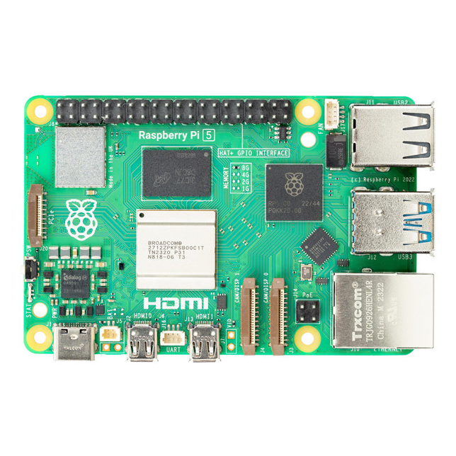
SC1111 - Raspberry Pi 5 4GB SBC 2.4GHz Cortex-A76 | Raspberry Pi | Desktop & Industrial
The Raspberry Pi 5 (SC1111, 4GB) is a single-board computer built upon a 64-bit quad-core 2.4 GHz Arm Cortex-A76 processor with 4GB of RAM on the full-size Raspberry Pi form factor. Per the official product data, its CPU delivers a two to three times increase in performance compared to Raspberry Pi 4, and it is the first full-size Raspberry Pi computer developed with silicon designed in-house by Raspberry Pi. Data verified as of 2026-09-13. A single-board computer (SBC) is a complete computer system integrated onto one printed circuit board, combining processor, memory, I/O interfaces, and power management without the need for a separate motherboard. Within the category hierarchy, the SBC sits between embedded compute modules and full desktop PCs, making it the standard platform for prototyping, education, and industrial edge deployments. Raspberry Pi popularized this form factor, and the Raspberry Pi 5 is its current full-size generation. Key characteristics of the SC1111 include the in-house-developed application processor running at 2.4 GHz, the substantial generational CPU performance uplift over Raspberry Pi 4, and the retained compatibility ethos of the full-size Raspberry Pi layout, which preserves the ecosystem of HAT add-on boards, cases, cameras, and displays that the community and industry have built over multiple generations. From a technical standpoint, the move to custom in-house silicon marks a strategic shift for Raspberry Pi: controlling the SoC design allows tighter integration between CPU, peripherals, and power architecture, which historically translates into better performance per watt and more predictable long-term supply. The quad-core Cortex-A76 core is an Armv8.2-A 64-bit architecture widely deployed in mainstream Android and Chromebook devices, so software toolchains, compilers, and Linux distributions are mature for this target. Typical applications include desktop-class computing and productivity use, industrial automation and edge data logging, robotics control, digital signage, and networked media or AI inference at the edge where local processing avoids cloud dependency. The 4GB memory configuration suits workloads such as lightweight servers, automation controllers, and multi-service IoT gateways. A practical design consideration: verify your power supply meets the board requirements from the official Raspberry Pi documentation before deployment, and confirm HAT mechanical and electrical compatibility when migrating from Raspberry Pi 4, since peripheral interfaces have been updated on this generation. What this page adds beyond the datasheet: a consolidated SC1111 price comparison across authorized distributors (Octopart lists 3 distributors, with PCBX quoting $68.56056 as of 2026-09-13), drop-in and functional alternative analysis within and beyond the Raspberry Pi 5 series, and practical deployment notes for desktop, industrial, and robotics use of this Arm Cortex-A76 single-board computer.
SC1112 - Raspberry Pi 5 8GB SBC, 2.4GHz Cortex-A76 | Raspberry Pi | Edge AI & IoT
The Raspberry Pi 5 (SC1112, 8GB) is a single-board computer built around a 64-bit quad-core 2.4GHz Arm Cortex-A76 processor (Broadcom BCM2712) with 8GB of LPDDR4X SDRAM, delivering two to three times the CPU performance of Raspberry Pi 4 on the standard full-size Raspberry Pi form factor. Data verified as of 2026-09-13. A single-board computer (SBC) is a complete computer fabricated on a single printed circuit board, integrating processor, memory, storage I/O, and connectivity. The Raspberry Pi 5 sits at the top of the Raspberry Pi single-board computer family, which belongs to the broader category of embedded computers, and was developed by Raspberry Pi with its own in-house silicon (BCM2712), a first for the company. Key features of the SC1112 include the 2.4GHz Cortex-A76 quad-core CPU, an 8GB memory configuration (a mid-tier option in the Raspberry Pi 5 series), and the standard 40-pin GPIO header for Hardware Attached on Top (HAT) expansion. Per the official Raspberry Pi product brief, the Pi 5 architecture enables two to three times the speed of other generations. From a technical standpoint, the BCM2712 integrates four Arm Cortex-A76 cores, a high-performance Armv8.2-A-class microarchitecture, with a modern GPU subsystem and I/O fabric. The 8GB LPDDR4X memory pool is the defining differentiator of SC1112 versus the 2GB, 4GB, and 8GB variants, allowing larger working sets for in-memory data processing, multi-container edge deployments, and desktop-class multitasking. Typical applications include edge AI inference and data logging, industrial IoT gateways, robotics control, and desktop-class computing where a compact, low-power Linux computer is required. The 40-pin GPIO header and broad OS support (Raspberry Pi OS, Ubuntu, and others) make it a strong fit for automation and prototyping. A practical design consideration: the higher CPU and memory throughput of Raspberry Pi 5 increases sustained power draw versus Raspberry Pi 4; plan the 5V USB-C power supply and thermal management (heatsink or fan) according to the official Raspberry Pi documentation. Beyond the datasheet, this page provides an SC1112 vs SC1111 (4GB) vs cross-brand SBC comparison, terminal-level 40-pin GPIO wiring reference, design notes, and sourcing information with prices refreshed as of 2026-09-13.
SC1113 - Raspberry Pi 5 16GB SBC, 2.4GHz Cortex-A76 | Raspberry Pi | Edge AI
The Raspberry Pi 5 (SC1113, 16GB) is a single-board computer built around a Broadcom BCM2712 SoC with a 4-core 64-bit Arm Cortex-A76 CPU running at 2.4GHz, 16GB of LPDDR4X SDRAM, and a VideoCore VII GPU, on the standard 85.6 x 56.5mm Raspberry Pi form factor. Data verified as of 2026-09-13. A single-board computer (SBC) is a complete computer system fabricated on a single printed circuit board, integrating the processor, memory, power management, storage interface, and I/O connectors on one board. SBCs sit within the broader category of embedded computers and are widely used where a full PC is unnecessary but general-purpose computing, networking, and expandable I/O are still required. Key features of the SC1113 include the largest memory option in the Raspberry Pi 5 family (16GB LPDDR4X, shared as system and GPU memory), dual 4Kp60-capable HDMI outputs, USB 3.0 and USB 2.0 ports, a PCI Express interface for NVMe storage, dual-band Wi-Fi and Bluetooth, Gigabit Ethernet, and the 40-pin GPIO header that supports HAT expansion boards. The updated power management IC integrates a real-time clock and charging circuitry, and heat dissipation was improved over the Raspberry Pi 4 generation. On the technical side, the VideoCore VII GPU supports OpenGL ES 3.1 and Vulkan 1.2, enabling modern graphics stacks and compute workloads. The faster BCM2712, camera/display interfaces (MIPI), and USB improvements over the predecessor make the Raspberry Pi 5 the most capable board in the Raspberry Pi lineup. The PCIe 2.0 x1 lane allows high-speed NVMe SSDs for storage-heavy applications, while the 40-pin header retains compatibility with the broad HAT ecosystem. Typical applications for the 16GB variant include edge AI inference where large models benefit from higher RAM, desktop computing with many open applications, lightweight virtualization or container hosting, media servers, and industrial gateways aggregating multiple data streams. A practical design consideration: use the recommended 5V/5A USB-C power supply; under sustained multi-core load the board draws significant power, and undervoltage from weak supplies is the most common cause of instability and SD card filesystem corruption. This page adds value beyond the datasheet by cross-referencing SC1113 against other Raspberry Pi 5 memory variants (SC1111 8GB, SC1112 4GB), detailing the 40-pin GPIO terminal map, and giving selection guidance for choosing between RAM tiers based on workload and budget.