FPGA & CPLD
Products (137)
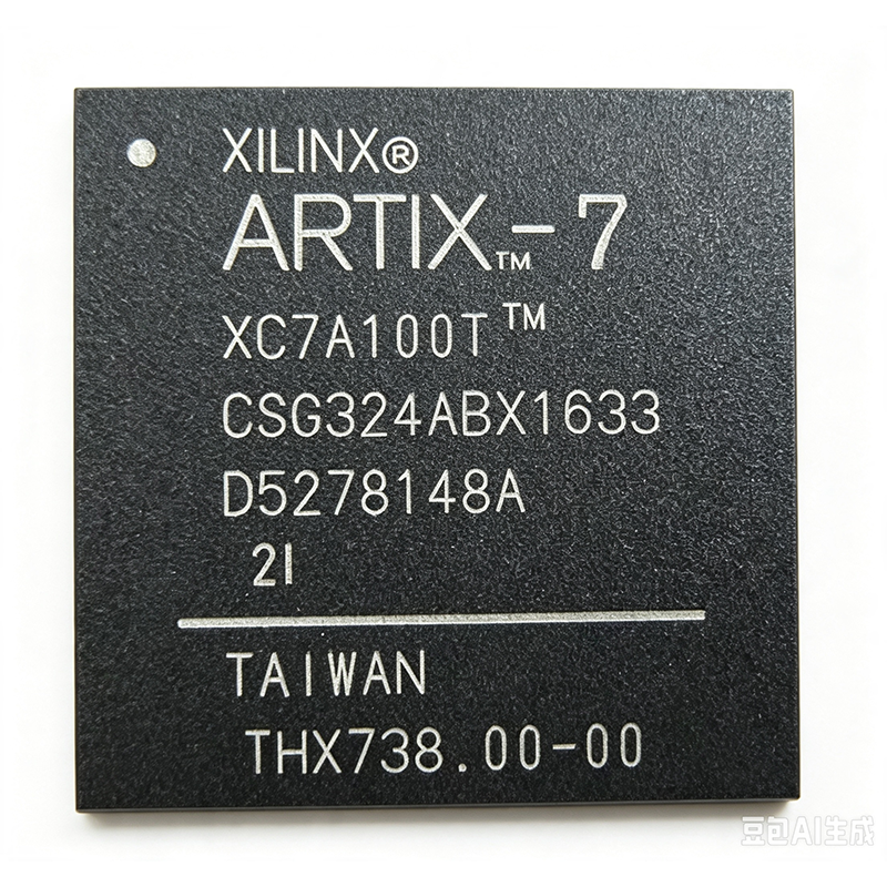
XC7A100T-1CSG324I-Q1 - Artix-7 FPGA, 101K Logic Cells | AMD
The AMD XC7A100T-1CSG324I-Q1 is an Artix-7 family FPGA delivering 101,440 logic cells, 240 DSP slices, and 4,860 Kb of block RAM in a 324-ball CSG (Chip Scale) package. It operates with a core voltage of 1.0V and supports up to 210 user I/O pins, making it a versatile choice for cost-sensitive, high-volume applications. An FPGA (Field-Programmable Gate Array) is a semiconductor device containing configurable logic blocks and programmable interconnects, allowing designers to implement custom digital logic after manufacturing. Within the broader hierarchy, an FPGA is a type of programmable logic device (PLD), which falls under the category of integrated circuits (ICs) and ultimately semiconductors. The Artix-7 family specifically targets low-power, high-performance applications, balancing logic density with power efficiency. Key features include 101,440 logic cells, 240 DSP48E1 slices for digital signal processing, and 4,860 Kb of block RAM. The device supports multiple I/O standards including LVCMOS, LVDS, and HSTL, and includes integrated PCIe blocks and GTP transceivers for high-speed serial communication. The -1 speed grade indicates a balanced performance level, while the I temperature grade supports operation from -40°C to +100°C (Tj). The XC7A100T-1CSG324I-Q1 is built on AMD's 28nm process technology, offering a favorable balance of performance, power, and cost. The CSG324 package provides a compact footprint with 324 balls, enabling dense PCB layouts. The device includes configuration support via JTAG, SPI, and BPI interfaces, and features AES bitstream encryption for design security. Typical applications include motor control in industrial automation, software-defined radio (SDR) for communications, medical imaging equipment, and automotive infotainment systems. The -Q1 suffix indicates automotive qualification, making it suitable for automotive applications requiring extended temperature ranges and reliability. When designing with this FPGA, careful attention must be paid to power supply decoupling, with multiple 100nF capacitors placed near each power pin. The configuration interface should be selected based on the system boot requirements, with SPI flash being the most common choice for standalone operation. This page synthesizes distributor pricing, drop-in alternatives, and practical design notes not found in the AMD datasheet, providing engineers with a comprehensive resource for design-in decisions.
XC7A100T-1FGG484I - Artix-7 FPGA, 285 I/O | AMD
The AMD XC7A100T-1FGG484I is an Artix-7 Field Programmable Gate Array (FPGA) from the 7 series family, offering a balance of low cost, small form factor, and high performance-per-watt for cost-sensitive, high-volume applications. It features 101,440 logic cells, 285 user I/Os, and 4,976,640 bits of block RAM, all in a 484-pin BGA (FGG484) package. The device operates on a 1V core voltage and is built on 28nm technology, providing a robust platform for a wide range of digital designs. An FPGA (Field Programmable Gate Array) is an integrated circuit that can be configured by the customer or designer after manufacturing. Unlike fixed-function ASICs, FPGAs contain an array of programmable logic blocks and a hierarchy of reconfigurable interconnects that allow the blocks to be wired together in different configurations. This flexibility makes FPGAs ideal for prototyping, low-to-mid volume production, and applications requiring hardware reconfiguration. In the system hierarchy, an FPGA sits above microcontrollers in complexity and parallelism, offering massive parallel processing capabilities for tasks like digital signal processing (DSP), high-speed I/O, and custom logic implementation. Key features of the XC7A100T-1FGG484I include 285 user I/Os, which provide ample connectivity for interfacing with external peripherals and memory. The device also integrates Mixed-Mode Clock Managers (MMCM) and Phase-Locked Loops (PLL) for robust clock generation and management. With 4,976,640 bits of block RAM, it can handle substantial data buffering and storage requirements. The Artix-7 family is optimized for highest performance-per-watt, making it suitable for power-sensitive applications. Technically, the Artix-7 series is built on a 28nm high-k metal gate (HKMG) process, offering a significant improvement in performance and power efficiency over older generations. The device supports various I/O standards, including LVCMOS, LVDS, and HSTL, enabling flexible interfacing. The FGG484 package provides a compact footprint while still offering a high pin count for complex designs. The 'I' suffix indicates an industrial temperature grade, allowing operation from -40°C to +100°C (Tj). Typical applications include software-defined radio, motor control, industrial networking, and video processing. The XC7A100T's combination of logic density, I/O count, and DSP capabilities makes it ideal for these mid-range applications where cost and power are critical. For example, in software-defined radio, the FPGA can handle multiple channels of digital down-conversion and filtering in parallel, offloading the host processor. When designing with this device, careful attention must be paid to power supply decoupling and sequencing. The FPGA requires multiple voltage rails (VCCINT, VCCAUX, VCCO), and proper sequencing is essential to avoid latch-up or damage. Refer to the Xilinx 7 Series FPGAs Power Management Application Note (XAPP) for detailed guidance.
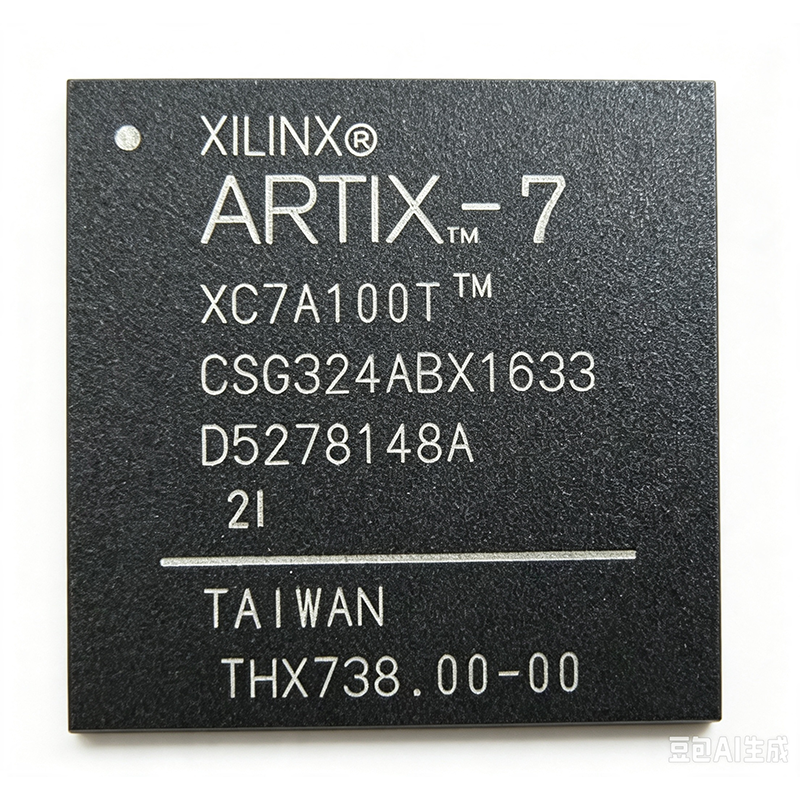
XC7A100T-2CSG324C - Artix-7 FPGA, 101K Logic Cells | AMD Xilinx
The AMD Xilinx XC7A100T-2CSG324C is a high-performance Artix-7 family FPGA delivering 101,440 logic cells, 240 DSP48E1 slices, and 4,860 Kb of block RAM in a 324-ball CSBGA (CSG324) package. It operates with a core voltage of 1.0V and supports I/O standards including LVCMOS, LVDS, and HSTL across 210 user I/O pins. Data verified as of 2026-08-04. An FPGA (Field-Programmable Gate Array) is a semiconductor device containing configurable logic blocks (CLBs), programmable interconnects, and I/O blocks that can be programmed after manufacturing to implement custom digital logic circuits. FPGAs sit within the broader category of programmable logic devices (PLDs), which are part of the application-specific integrated circuit (ASIC) family, but unlike ASICs, FPGAs offer reconfigurability, making them ideal for prototyping, low-volume production, and applications requiring in-field updates. Key features of the XC7A100T-2CSG324C include 101,440 logic cells, 240 DSP slices for high-speed signal processing, 4,860 Kb of block RAM, and 6 CMTs (Clock Management Tiles) providing PLL and MMCM for robust clock generation. The device supports PCIe Gen2 x1, Gigabit Ethernet, and DDR3 memory interfaces, making it suitable for a wide range of embedded and communications applications. The -2 speed grade offers a balance of performance and power, with a maximum clock frequency of 400 MHz for block RAM and 600 MHz for I/O. The Artix-7 architecture is built on a 28nm high-k metal gate (HKMG) process, delivering low static power consumption and high logic density. The device includes hardened memory controllers for DDR3, and its SelectIO technology supports up to 1.25 Gbps LVDS, enabling high-speed data transfer. The CSG324 package measures 15x15 mm with a 0.8 mm ball pitch, providing a compact footprint for space-constrained designs. Typical applications include software-defined radio (SDR), motor control, industrial Ethernet, medical imaging, and video processing. The XC7A100T-2CSG324C is particularly suited for applications requiring high DSP throughput and moderate logic capacity, such as digital signal processing in radar and communication systems. When designing with this FPGA, careful attention must be paid to power supply decoupling, with multiple 100nF capacitors placed near each power pin, and to thermal management, as the device can dissipate up to 2.5W under full utilization. The configuration bitstream can be stored in SPI flash, and the device supports multi-boot for remote updates. This page synthesizes distributor pricing, drop-in alternatives, and practical design notes not found in the AMD Xilinx datasheet, providing engineers with a comprehensive resource for selecting and implementing the XC7A100T-2CSG324C.
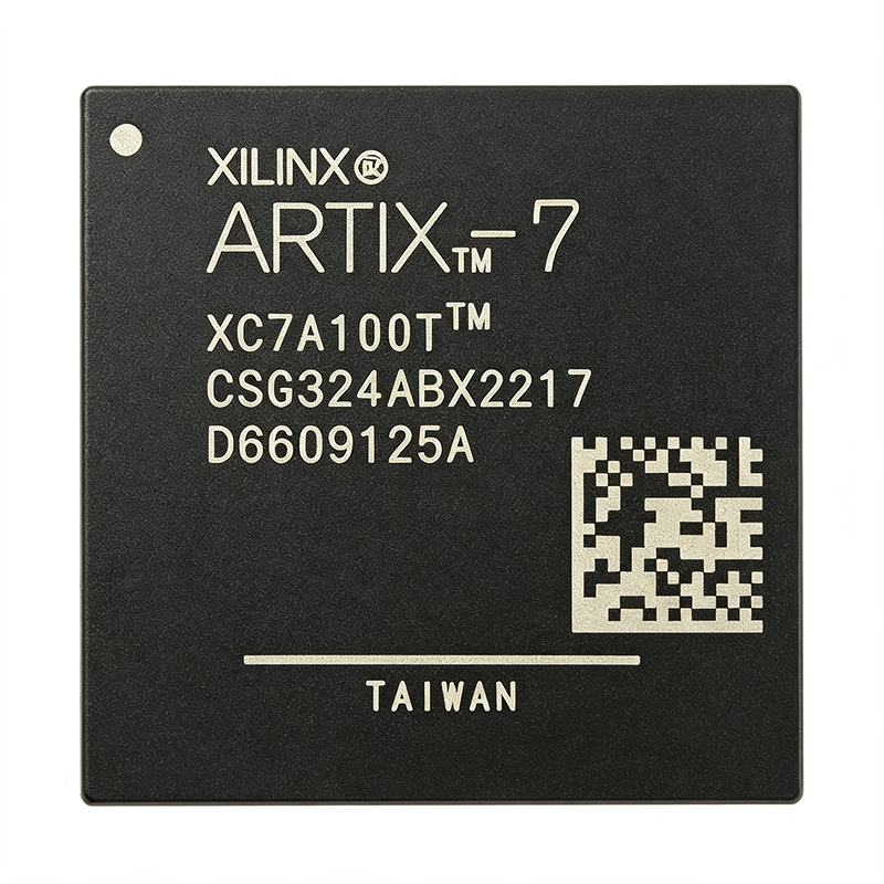
XC7A100T-2CSG324I - Artix-7 FPGA, 101K Logic Cells | AMD Xilinx
The AMD Xilinx XC7A100T-2CSG324I is a high-performance Artix-7 family FPGA delivering 101,440 logic cells, 240 DSP slices, and 4,860 Kb of block RAM in a 324-ball CSG (Chip-Scale BGA) package. It operates over the industrial temperature range (-40°C to +100°C) and is designed for cost-sensitive, high-volume applications requiring low power and high throughput. An FPGA (Field-Programmable Gate Array) is a semiconductor device containing a matrix of configurable logic blocks (CLBs) connected by programmable interconnects, allowing designers to implement custom digital logic circuits after manufacturing. FPGAs sit within the broader category of programmable logic devices (PLDs), which are part of the larger family of integrated circuits (ICs). Unlike fixed-function ASICs, FPGAs offer reconfigurability, enabling rapid prototyping and field upgrades, making them essential in applications ranging from embedded vision to software-defined radio. Key features of the XC7A100T-2CSG324I include 285,120 flip-flops, 240 DSP48E1 slices (each capable of 25x18 multiplication), and 135 Block RAM blocks (36 Kb each) totaling 4,860 Kb. The device supports up to 300 user I/O pins with support for multiple I/O standards including LVCMOS, LVDS, and HSTL. It integrates a 12-bit, 1 MSPS XADC for analog monitoring and supports PCIe Gen2 x1 and 10/100/1000 Ethernet via hardened blocks. The -2 speed grade provides balanced performance, with internal clock speeds up to 628 MHz. The Artix-7 architecture is built on a 28 nm high-k metal gate (HKMG) process, offering a 50% lower static power compared to previous generations. The device includes a unified configuration interface supporting JTAG, SelectMAP, and Quad-SPI flash programming. Its low-power transceivers (up to 16 GTP transceivers at 6.6 Gbps) enable high-speed serial connectivity for applications like video over SDI and CPRI. Typical applications include software-defined radio (SDR), medical imaging, motor control, and industrial Ethernet. The XC7A100T-2CSG324I is particularly suited for designs requiring high logic density with moderate I/O counts, such as camera-based vision systems and test equipment. Its industrial temperature grade makes it reliable for harsh environments. For detailed specifications, refer to the official AMD Xilinx datasheet (DS181) and the Artix-7 FPGA product page at https://www.xilinx.com/products/silicon-devices/fpga/artix-7.html. When designing with this FPGA, careful attention must be paid to power supply decoupling and PCB layout to ensure signal integrity at high speeds. The device requires multiple supply rails (VCCINT, VCCAUX, VCCO) with specific sequencing, and the use of the XADC for thermal monitoring is recommended to prevent overheating.
XC7A100T-2FBG484I - Artix-7 FPGA, 101K Logic Cells | AMD
The AMD XC7A100T-2FBG484I is a high-performance Artix-7 Field Programmable Gate Array (FPGA) from the 7 Series family, offering 101,440 logic cells, 285 user I/Os, and 4,976,640 bits of block RAM in a 484-ball FBGA package. It operates over an industrial temperature range of -40°C to +100°C and is designed for cost-sensitive applications requiring high performance-per-watt. An FPGA (Field Programmable Gate Array) is an integrated circuit that can be configured by the customer after manufacturing to implement arbitrary digital logic functions. FPGAs sit between ASICs (application-specific ICs) and microprocessors in the design hierarchy: they offer the parallelism and determinism of custom hardware with the reconfigurability of software. The Artix-7 family is optimized for the lowest power and cost at 28nm, making it a popular choice for embedded vision, software-defined radio, and industrial automation. Key features of the XC7A100T-2FBG484I include 285 user I/Os, 4,976,640 bits of block RAM, 240 DSP slices, and support for MMCM and PLL clock management. The -2 speed grade provides a maximum clock frequency of 628 MHz, while the industrial temperature rating ensures reliable operation in harsh environments. The device supports VCCINT from 0.95V to 1.05V, enabling flexible power supply design. Architecturally, the Artix-7 fabric is built on a 28nm high-k metal gate (HKMG) process, delivering a 50% reduction in power consumption compared to previous generations. The device integrates AMS (Analog Mixed Signal) blocks, including a 12-bit 1 MSPS ADC, for on-chip monitoring of voltage and temperature. This integration reduces external component count and simplifies board design. Typical applications include software-defined radio, motor control, industrial Ethernet, and medical imaging. The 484-ball FBGA package provides a balanced pin count for medium-complexity designs, while the industrial temperature range makes it suitable for outdoor and automotive-adjacent deployments. When designing with this device, ensure adequate decoupling on all power rails (VCCINT, VCCAUX, VCCO) and follow AMD's power-on sequencing guidelines to avoid latch-up. The configuration bitstream can be stored in external SPI flash or loaded via JTAG, with support for multi-boot for remote updates.
XC7A100T-2FGG484I - Artix-7 FPGA, 285 I/O | AMD
The AMD XC7A100T-2FGG484I is a high-performance Artix-7 Field Programmable Gate Array (FPGA) in a 484-ball FBGA package. It delivers 101,440 logic cells, 285 user I/Os, and 4,976,640 bits of block RAM, operating from a 0.95V to 1.05V core supply. This industrial-temperature (-40°C to +100°C) device is optimized for cost-sensitive applications requiring high performance-per-watt. An FPGA is an integrated circuit whose logic fabric can be reconfigured after manufacturing. Unlike fixed-function ASICs, FPGAs contain programmable logic blocks, interconnects, and I/O cells that implement custom digital circuits. The Artix-7 family sits between the smaller Spartan-7 and larger Kintex-7 in AMD's 7-series, balancing logic density, DSP capability, and transceiver performance for mid-range applications. Key features include 285 I/O pins supporting various voltage standards, 240 DSP48E1 slices for signal processing, and 10 clock management tiles (CMTs) with MMCM and PLL. The device supports MicroBlaze soft processor cores and DDR3 memory interfaces up to 1,066 Mb/s. Its 28nm process technology enables low power consumption while maintaining high logic utilization. The XC7A100T-2FGG484I integrates AMS (Analog Mixed Signal) blocks with 12-bit ADC, enabling on-chip voltage and temperature monitoring. The fabric runs at up to 628 MHz, and the device supports partial reconfiguration for flexible system updates. Industrial temperature rating ensures reliable operation in harsh environments. Typical applications include motor control, industrial networking, medical imaging, and software-defined radio. The 484-ball package provides a balanced pin count for moderate I/O requirements while maintaining signal integrity. For designs needing more I/O, the FGG676 variant offers additional connectivity. When designing with this FPGA, proper power sequencing and decoupling are critical. The device requires multiple supply rails (VCCINT, VCCAUX, VCCO) with specific ramp rates. Use AMD's Vivado Design Suite for configuration and the provided pinout files (UG475) for PCB layout.
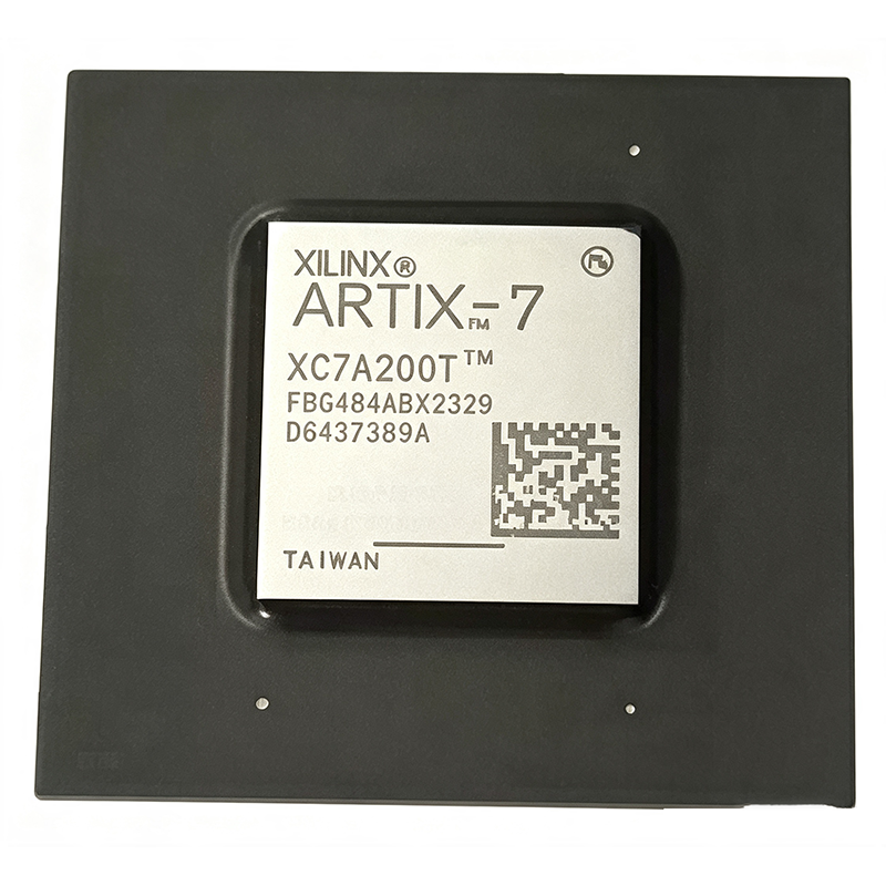
XC7A200T-1FBG484I - 740K Logic Cells FPGA | AMD Xilinx
The AMD Xilinx XC7A200T-1FBG484I is a high-performance Artix-7 family FPGA delivering 740K logic cells, 215K logic slices, and 13 Mb of block RAM in a 484-ball FBGA package. It operates from 0.95V to 1.05V core voltage and supports up to 285 user I/O pins with multiple I/O standards including LVCMOS, LVDS, and HSTL. The device features 740 DSP48E1 slices for high-speed digital signal processing and 10 clock management tiles (CMTs) for robust clock generation and distribution. An FPGA (Field-Programmable Gate Array) is a semiconductor device containing programmable logic blocks and interconnects that can be configured after manufacturing to implement custom digital circuits. FPGAs sit between ASICs (application-specific integrated circuits) and microprocessors in the design hierarchy, offering the flexibility of software-defined hardware with the parallelism of dedicated logic. The Artix-7 family is optimized for cost-sensitive, high-volume applications requiring high logic density and low power, positioned below the Kintex-7 and Virtex-7 families in AMD's 7-series portfolio. Key features include 285 user I/O pins supporting up to 1.25 Gbps LVDS, 740 DSP48E1 slices with 25x18 multiplier capability, and 10 CMTs providing PLL and MMCM functions. The device also offers 13 Mb of block RAM organized as 365 36Kb blocks, enabling substantial on-chip data storage. The -1 speed grade provides balanced performance with 550 MHz maximum clock frequency, while the industrial temperature range (-40C to +100C) ensures reliable operation in harsh environments. The XC7A200T-1FBG484I is built on AMD's 28nm high-k metal gate (HKMG) process technology, delivering high performance with low static power. The architecture includes configurable logic blocks (CLBs) with 6-input look-up tables (LUTs), dedicated carry chains for arithmetic functions, and shift register capabilities. The device supports partial reconfiguration, allowing dynamic updates to logic functions without full device reprogramming, which is valuable for adaptive systems. Typical applications include software-defined radio (SDR), medical imaging, industrial motor control, and high-performance computing acceleration. The high DSP count and low-latency I/O make it ideal for real-time signal processing in communications and defense systems. The 484-ball FBGA package with 1.0mm ball pitch enables compact PCB designs while providing adequate thermal dissipation for moderate power levels. When designing with this FPGA, ensure adequate decoupling capacitors on all power rails (VCCINT, VCCAUX, VCCO) and follow AMD's PCB design guidelines for high-speed I/O. The configuration interface supports multiple modes including JTAG, SPI, and SelectMAP, allowing flexible system integration. Power sequencing must follow the recommended ramp rates to avoid latch-up or configuration failures.
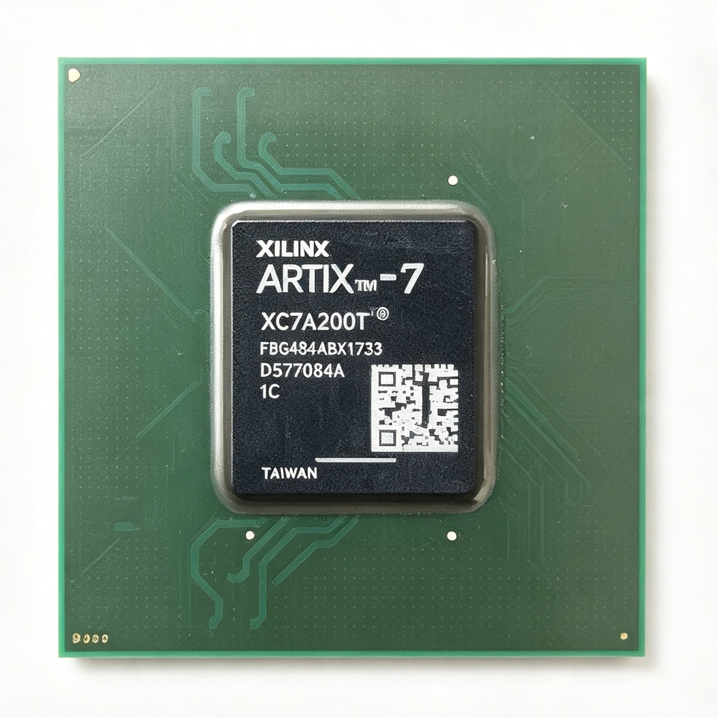
XC7A200T-1FBG676I - 740K Logic Cells FPGA | AMD Xilinx | FBG676
The AMD Xilinx XC7A200T-1FBG676I is a high-performance Artix-7 family FPGA delivering 740K logic cells, 215,360 logic slices, and 13,140 Kb of Block RAM in a 676-ball FCBGA (FBG676) package. It operates with a core voltage of 1.0V and supports I/O standards up to 3.3V, making it suitable for a wide range of high-speed digital designs. Data verified as of 2026-08-05. An FPGA (Field-Programmable Gate Array) is an integrated circuit that can be configured by the designer after manufacturing, offering reconfigurable logic blocks and programmable interconnects. FPGAs sit within the broader hierarchy of programmable logic devices (PLDs), which are a subset of digital integrated circuits. They provide a flexible alternative to ASICs, enabling rapid prototyping and hardware acceleration without the high NRE costs of custom silicon. Key features include 740K logic cells, 365 DSP48E1 slices, 10.5 Mb of distributed RAM, and 13,140 Kb of Block RAM. The device supports up to 400 I/O pins with SelectIO technology, offering programmable I/O standards and speeds. It also includes integrated PCIe blocks, Gigabit Transceivers (GTX) for high-speed serial communication, and a XADC for analog-to-digital conversion, providing a comprehensive platform for complex digital systems. The Artix-7 architecture is built on a 28nm high-k metal gate (HKMG) process, balancing performance and power efficiency. The device features a configurable logic block (CLB) structure with 6-input LUTs, dedicated carry chains, and flip-flops, enabling efficient implementation of complex logic functions. The DSP48E1 slices support high-speed arithmetic operations, while the Block RAM provides on-chip storage for data buffering and FIFO implementations. Typical applications include software-defined radio (SDR), medical imaging, industrial motor control, and high-performance computing acceleration. The high logic density and DSP resources make it ideal for signal processing tasks, while the transceivers enable high-speed data communication in networking and broadcast equipment. When designing with this FPGA, careful attention must be paid to power supply decoupling and thermal management. The device requires multiple supply rails (VCCINT, VCCAUX, VCCO) with proper sequencing, and the 676-ball BGA package demands a multi-layer PCB with adequate thermal vias for heat dissipation. This page synthesizes distributor pricing, drop-in alternatives, and practical design notes not found in the AMD datasheet.
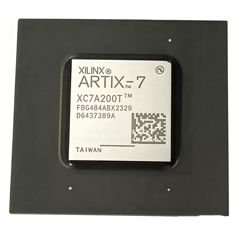
XC7A200T-2FBG484C - Artix-7 FPGA 740K Logic Cells | AMD Xilinx
The AMD Xilinx XC7A200T-2FBG484C is a high-performance Artix-7 family FPGA delivering 740K logic cells, 215K logic slices, and 13 Mb of block RAM in a 484-ball FBGA package. It operates with a core voltage of 1.0V and supports I/O standards from 1.2V to 3.3V, making it suitable for a wide range of applications. Data verified as of 2026-08-04. An FPGA (Field-Programmable Gate Array) is an integrated circuit that can be configured by the customer or designer after manufacturing. It consists of programmable logic blocks, configurable interconnects, and I/O blocks, allowing for flexible implementation of digital circuits. FPGAs sit within the broader category of programmable logic devices (PLDs), which are part of the semiconductor industry. They are used in applications requiring parallel processing, high-speed I/O, and reconfigurable logic, such as communications, industrial automation, and aerospace. Key features of the XC7A200T-2FBG484C include 740K logic cells, 215K logic slices, 13 Mb of block RAM, 740 DSP slices, and 10.3 Mb of distributed RAM. It also features 16 GTX transceivers supporting up to 6.6 Gbps, 10 clock management tiles (CMTs), and 285 user I/O pins. The device supports multiple I/O standards including LVCMOS, LVDS, and HSTL, and includes hardened memory controllers for DDR3 and DDR4. The Artix-7 architecture is built on a 28nm high-k metal gate (HKMG) process, offering a balance of performance, power, and cost. The device includes advanced clocking resources, such as PLLs and MMCMs, and supports partial reconfiguration for dynamic logic updates. The 484-ball FBGA package provides a compact footprint with excellent thermal and electrical characteristics, enabling high-density designs. Typical applications include software-defined radio (SDR), medical imaging, motor control, and high-performance computing. The high logic density and DSP slices make it ideal for signal processing, while the GTX transceivers support high-speed serial communication in networking and video applications. When designing with this FPGA, careful attention must be paid to power supply decoupling and thermal management. The device requires multiple supply rails (VCCINT, VCCAUX, VCCO) and a proper power-up sequence. Use the Xilinx Power Estimator (XPE) to calculate power consumption and design an appropriate thermal solution. This page synthesizes distributor pricing, drop-in alternatives, and practical design notes not found in the AMD Xilinx datasheet, providing a comprehensive resource for engineers.
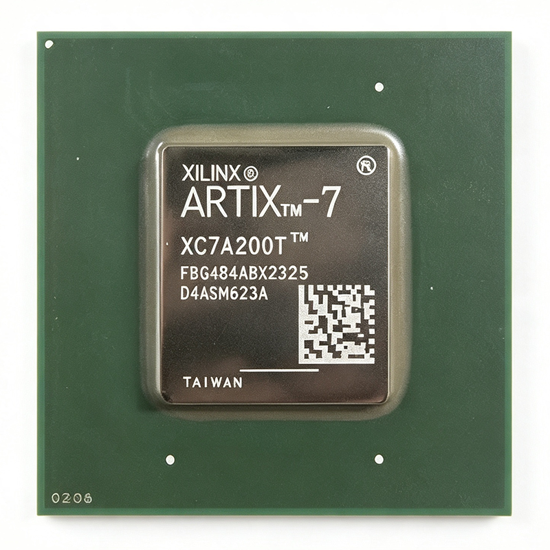
XC7A200T-2FBG484I - Artix-7 FPGA 215K Logic Cells | AMD Xilinx
The AMD Xilinx XC7A200T-2FBG484I is a high-performance Artix-7 family FPGA featuring 215,360 logic cells, 16,825 CLBs, and 13,455,360 bits of Block RAM, packaged in a 484-ball FBGA (FBG484) with a -2 speed grade and industrial temperature range (-40°C to +100°C). It delivers 285 user I/O pins, making it ideal for high-bandwidth signal processing and connectivity applications. An FPGA (Field-Programmable Gate Array) is a semiconductor device containing programmable logic blocks and interconnects that can be configured after manufacturing to implement custom digital circuits. FPGAs sit within the broader category of programmable logic devices (PLDs), which are part of the application-specific integrated circuit (ASIC) family, but offer reconfigurability that ASICs lack. The Artix-7 family is positioned as a mid-range FPGA optimized for cost-sensitive, high-volume applications requiring high-speed transceivers and DSP capabilities. Key features include 740 DSP48E1 slices for high-throughput digital signal processing, 16 high-speed transceivers supporting up to 6.6 Gb/s, and 285 I/O pins with support for multiple I/O standards including LVCMOS, LVDS, and HSTL. The device also integrates a PCIe Gen2 block, 10/100/1000 Ethernet MACs, and an analog-to-digital converter (XADC) for system monitoring. The -2 speed grade provides balanced performance for logic and I/O, while the industrial temperature range ensures reliable operation in harsh environments. Architecturally, the XC7A200T is built on the 28nm high-k metal gate (HKMG) process, offering a 50% lower power footprint compared to previous generations. The configurable logic blocks (CLBs) contain 6-input look-up tables (LUTs) and dual flip-flops, enabling efficient implementation of complex logic functions. The device supports partial reconfiguration, allowing dynamic updates to specific regions without disrupting the entire design. Typical applications include software-defined radio (SDR), medical imaging, industrial motor control, and high-performance computing acceleration. The high transceiver count and DSP resources make it particularly suited for communications infrastructure, such as LTE/5G base stations and network switches, where high-speed serial links and parallel processing are essential. When designing with this FPGA, careful attention must be paid to power supply decoupling and thermal management. The device requires multiple voltage rails (VCCINT, VCCAUX, VCCO) with proper sequencing, and the FBG484 package has a thermal resistance of 8.4°C/W (theta_JA) that necessitates adequate airflow or heatsinking for high-utilization designs.
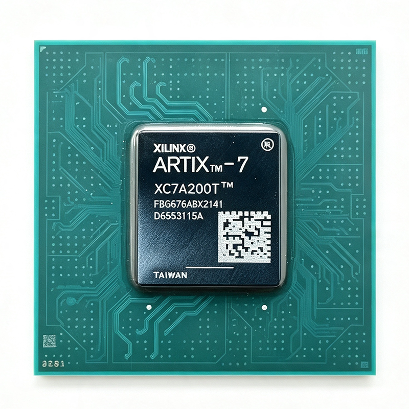
XC7A200T-2FBG676C - 740K Logic Cells FPGA | AMD Xilinx
The AMD Xilinx XC7A200T-2FBG676C is a high-performance Artix-7 family FPGA delivering 740K logic cells, 215K logic slices, and 13 Mb of block RAM in a 676-ball FCBGA (FBG676) package. It operates with a core voltage of 1.0V and supports I/O standards including LVCMOS, LVDS, and HSTL across 400 user I/O pins. An FPGA (Field-Programmable Gate Array) is a semiconductor device containing programmable logic blocks and programmable interconnects that can be configured after manufacturing to implement any digital logic function. FPGAs sit within the broader hierarchy of programmable logic devices (PLDs), which are a subset of integrated circuits (ICs). Unlike fixed-function ASICs, FPGAs offer reconfigurability, making them ideal for prototyping, rapid iteration, and applications requiring in-field updates. The Artix-7 family is optimized for cost-sensitive, high-volume applications requiring high logic density and low power. Key features include 740K logic cells, 215K logic slices, 13 Mb of block RAM, 740 DSP slices, and 16 high-speed transceivers supporting up to 6.6 Gbps. The device also integrates a 12-bit 1 MSPS ADC (XADC) for on-chip temperature and voltage monitoring. The FBG676 package provides 400 user I/O pins with support for multiple I/O standards, enabling flexible board design. The XC7A200T-2FBG676C is built on the 28nm high-k metal gate (HKMG) process technology, balancing performance and power efficiency. The -2 speed grade offers a balance of performance and cost, with internal clock speeds up to 628 MHz. The device supports partial reconfiguration, allowing dynamic updates to specific logic regions without disrupting the entire design. Typical applications include software-defined radio (SDR), medical imaging, industrial motor control, and high-performance computing acceleration. The high logic density and DSP slices make it suitable for digital signal processing (DSP) tasks such as FFTs and filters, while the transceivers enable high-speed serial communication in networking equipment. When designing with this FPGA, ensure adequate decoupling capacitors on all power rails (VCCINT, VCCAUX, VCCO) and follow the recommended power-up sequence. The configuration interface (JTAG, SPI, or BPI) must be carefully planned to support the required boot mode and update strategy.
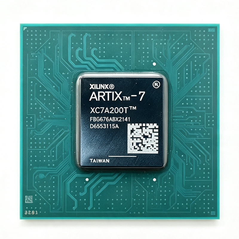
XC7A200T-2FBG676I - 740K Logic Cells FPGA | AMD Xilinx
The AMD Xilinx XC7A200T-2FBG676I is a high-performance Artix-7 family FPGA delivering 740K logic cells, 215,360 logic slices, and 13,140 Kb of Block RAM in a 676-ball FCBGA (FBG676) package. It operates with a core voltage of 1.0V and supports I/O standards including LVCMOS, LVDS, and HSTL, with up to 400 user I/O pins. The device is designed for high-bandwidth, low-power applications requiring substantial programmable logic and DSP resources. An FPGA (Field-Programmable Gate Array) is a semiconductor device containing configurable logic blocks (CLBs) and programmable interconnects that can be programmed after manufacturing to implement arbitrary digital logic functions. FPGAs sit within the broader category of programmable logic devices (PLDs), which are part of the larger family of integrated circuits (ICs). Unlike fixed-function ASICs, FPGAs offer reconfigurability, making them ideal for prototyping, rapid iteration, and applications where requirements may evolve. The Artix-7 family is positioned as a mid-range FPGA balancing logic density, DSP capability, and power efficiency, bridging the gap between low-cost Spartan-7 and high-performance Kintex-7 devices. Key features of the XC7A200T-2FBG676I include 740 DSP48E1 slices for high-speed digital signal processing, 10.5 Mb of distributed RAM, and support for PCIe Gen2 x4 and 16 high-speed transceivers running at up to 6.6 Gb/s. The device also integrates a 12-bit 1 MSPS XADC for analog monitoring, and supports partial reconfiguration for dynamic logic updates. With a speed grade of -2, it offers balanced performance for a wide range of applications. Architecturally, the XC7A200T is built on a 28nm high-k metal gate (HKMG) process, providing a 50% power reduction compared to previous generations. The device features a flexible clocking architecture with 10 CMTs (Clock Management Tiles) and 32 global clock buffers, enabling complex multi-clock domain designs. The FBG676 package provides 676 balls with a 27mm x 27mm body, offering excellent thermal and electrical characteristics for high-density designs. Typical applications include software-defined radio (SDR), medical imaging, industrial motor control, and high-performance computing acceleration. The device's high logic density and DSP resources make it suitable for implementing complex algorithms such as FFTs, filters, and image processing pipelines. Its transceiver capability supports high-speed serial protocols like PCIe, Gigabit Ethernet, and CPRI. When designing with this FPGA, careful attention must be paid to power supply decoupling and thermal management. The device requires multiple supply rails (VCCINT, VCCAUX, VCCO) with proper sequencing, and a heatsink or active cooling is recommended for high-utilization designs. Use AMD's Vivado Design Suite for configuration and implementation, and refer to the Artix-7 FPGA Data Sheet (DS181) for detailed specifications.
XC7A200T-2FFG1156I - Artix-7 FPGA 215K Logic Cells | AMD
The AMD XC7A200T-2FFG1156I is a member of the Artix-7 FPGA family, offering a balance of high performance, low power, and cost efficiency for a wide range of applications. It features 215,360 logic cells, 500 user I/Os, and 13,455,360 block RAM bits, all in a 1156-ball FCBGA package. Operating from a 0.95V to 1.05V core voltage, this device is designed for systems requiring substantial programmable logic and I/O capability. An FPGA (Field-Programmable Gate Array) is an integrated circuit that can be configured by the designer after manufacturing, allowing for custom digital logic implementations. FPGAs sit within the broader category of programmable logic devices (PLDs), which are part of the semiconductor industry. They offer flexibility and parallel processing capabilities that are often superior to microprocessors for specific tasks, making them essential in prototyping, signal processing, and hardware acceleration. Key features of the XC7A200T-2FFG1156I include 740 DSP slices for high-speed digital signal processing, 10 clock management tiles (CMTs) with MMCM and PLL for robust clock generation, and support for MicroBlaze soft-core processors. The device also integrates analog-to-digital converters (XADC) for on-chip temperature and voltage monitoring. With a maximum operating frequency of 628 MHz, it delivers high performance for demanding logic designs. Built on 28nm technology, the Artix-7 family provides the highest performance-per-watt fabric in its class. The device supports various I/O standards, including LVCMOS, LVDS, and HSTL, and features high-speed transceivers for serial communication. The 1156-ball FCBGA package offers excellent thermal and electrical characteristics, enabling reliable operation in industrial temperature ranges (-40°C to +100°C). Typical applications include software-defined radio, motor control, medical imaging, and aerospace systems. The combination of logic density, DSP capability, and I/O flexibility makes it suitable for both prototyping and production deployments. Designers can leverage AMD's Vivado Design Suite for comprehensive development support. When designing with this FPGA, careful attention to power supply decoupling and thermal management is essential. The device requires multiple supply rails, and proper sequencing is critical to ensure reliable operation. Additionally, utilizing the on-chip XADC for monitoring can enhance system reliability.
XC7A200T-2FGG484I - Artix-7 FPGA 215K Logic Cells | AMD
The AMD XC7A200T-2FGG484I is a high-performance Artix-7 Field Programmable Gate Array (FPGA) from the cost-optimized 28nm family, delivering the highest performance-per-watt fabric in its class. It features 215,360 logic cells, 16825 CLBs, and 13,455,360 bits of block RAM, packaged in a 484-ball Fine-Pitch Ball Grid Array (FBGA) with an industrial temperature range of -40°C to +100°C. This device operates from a nominal 1.0V core supply (0.95V to 1.05V) and supports up to 285 user I/O pins. An FPGA (Field Programmable Gate Array) is an integrated circuit that can be configured by the designer after manufacturing, allowing for custom digital logic implementation. FPGAs sit within the broader hierarchy of programmable logic devices, which are part of the semiconductor industry. Unlike fixed-function ASICs, FPGAs offer reconfigurability, making them ideal for prototyping, low-to-mid volume production, and applications requiring field updates. The Artix-7 family specifically targets cost-sensitive, high-volume applications where performance-per-watt and low power are critical. Key features of the XC7A200T-2FGG484I include 740 DSP slices for high-speed digital signal processing, 10 clock management tiles (CMTs) with MMCM and PLL, and support for various configuration interfaces including JTAG, SPI, and BPI. The -2 speed grade offers a balanced performance point, with the -3 being the highest performance and -1/-1LI/-2L optimized for lower static power. The device also integrates analog mixed-signal (AMS) blocks with a 12-bit 1MSPS ADC for on-chip monitoring. Technically, the Artix-7 architecture is built on a 28nm high-k metal gate (HKMG) process, providing a significant leap in logic density and power efficiency over previous generations. The fabric includes 6-input look-up tables (LUTs), dedicated carry chains, and shift register logic, enabling efficient implementation of complex datapaths. The block RAM can be configured in various aspect ratios, and the DSP48E1 slices support 25x18 multiplication with 48-bit accumulation, ideal for filter and FFT implementations. Typical applications include software-defined radio, motor control, medical imaging, and industrial networking. The high I/O count and DSP resources make it suitable for video processing, high-speed data acquisition, and aerospace/defense systems requiring reconfigurable logic. The industrial temperature grade ensures reliable operation in harsh environments. When designing with this device, careful attention must be paid to power supply decoupling, with multiple 1.0V core and 1.8V auxiliary rails requiring proper filtering. Configuration bitstream storage in external SPI flash is recommended for production, and the device supports partial reconfiguration for dynamic logic updates.
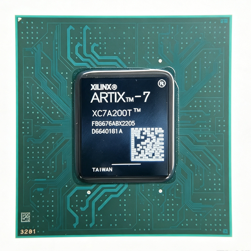
XC7A200T-3FBG676I - Artix-7 FPGA, 740K Logic Cells | AMD
The AMD XC7A200T-3FBG676I is a high-performance Artix-7 family FPGA featuring 740K logic cells, 13.3 Mb of Block RAM, and 740 DSP slices in a 676-ball FCBGA package. It operates with a core voltage of 1.0V and supports I/O standards up to 3.3V. Data verified as of 2026-08-04. An FPGA (Field-Programmable Gate Array) is an integrated circuit that can be configured by the customer after manufacturing to implement any digital logic function. FPGAs sit between ASICs (application-specific) and microprocessors (fixed instruction set) in the design hierarchy, offering reconfigurability and parallel processing. The Artix-7 family is optimized for high-performance, low-power applications, balancing logic density, DSP capability, and I/O flexibility. Key features include 740K logic cells, 13.3 Mb of Block RAM, 740 DSP slices, and support for PCIe Gen2, Gigabit transceivers, and DDR3 memory interfaces. The -3 speed grade provides the highest performance in the Artix-7 family, with 6.6 Gb/s transceivers and 550 MHz clocking. The industrial temperature grade (-I) supports operation from -40C to +100C, making it suitable for harsh environments. The XC7A200T-3FBG676I is built on 28nm process technology, offering a balance of performance and power efficiency. It includes hardened memory controllers for DDR3, and configurable logic blocks with 6-input LUTs. The device supports partial reconfiguration and has built-in analog-to-digital converter (XADC) for system monitoring. Typical applications include software-defined radio, medical imaging, industrial motor control, and high-performance computing acceleration. The high DSP count and transceiver speed make it ideal for signal processing and high-throughput data paths. When designing with this FPGA, ensure adequate decoupling capacitors on all power rails and follow the recommended power-up sequence. The configuration bitstream can be stored in external SPI flash or loaded via JTAG. Thermal management is critical at high utilization; use the exposed pad and proper airflow. This page synthesizes distributor pricing, drop-in alternatives, and practical design notes not found in the AMD datasheet, providing a comprehensive resource for engineers evaluating the XC7A200T-3FBG676I.

XC7A35T-1FGG484I - Artix-7 FPGA, 250 I/O | AMD
The AMD XC7A35T-1FGG484I is an Artix-7 Field Programmable Gate Array (FPGA) from the 28nm Artix-7 family, offering 33,280 logic cells, 250 user I/Os, and 1,843,200 bits of block RAM in a 484-ball FBGA (23x23mm) package. It operates over the industrial temperature range of -40°C to +100°C (TJ) and is designed for cost-sensitive, high-volume applications requiring high performance-per-watt. An FPGA (Field Programmable Gate Array) is an integrated circuit that can be configured by the customer after manufacturing to implement any digital logic function. Unlike fixed-function ASICs, FPGAs contain programmable logic blocks, configurable I/O, and routing resources that allow designers to implement complex digital systems in hardware. The Artix-7 family sits between the low-cost Spartan-7 and the higher-performance Kintex-7 in AMD's 7-series portfolio, targeting applications where cost and power efficiency are paramount. Key features of the XC7A35T-1FGG484I include 250 user I/O pins, 2,600 Configurable Logic Blocks (CLBs), 33,280 logic cells, and 1,843,200 total RAM bits. The device integrates five Clock Management Tiles (CMTs) with MMCM and PLL blocks for flexible clock generation, and supports multiple I/O standards including LVCMOS, LVDS, and HSTL. The 484-ball FBGA package provides a compact 23x23mm footprint with 0.8mm ball pitch, enabling dense PCB layouts. The Artix-7 architecture is built on a 28nm high-k metal gate (HKMG) process technology, delivering up to 50% lower power consumption compared to previous generations. The device supports partial reconfiguration, allowing dynamic updates to logic functions without powering down the system. With support for AMD Vivado Design Suite, designers can implement complex designs using a mature and comprehensive toolchain. Typical applications include industrial motor control, medical imaging, software-defined radio, video processing, and automotive driver assistance systems. The industrial temperature grade makes it suitable for harsh environments where reliability is critical. When designing with this device, ensure adequate decoupling capacitors on all power rails and follow the PCB layout guidelines in UG475 for the 484-FBGA package to maintain signal integrity.
XC7A35T-2CPG236I - Artix-7 FPGA 33280 Logic Cells | AMD
The AMD XC7A35T-2CPG236I is an Artix-7 Field Programmable Gate Array (FPGA) from the 7 series family, offering 33,280 logic cells, 2,600 Configurable Logic Blocks (CLBs)/LABs, and 106 user I/O pins. It is housed in a 238-ball LFBGA/CSPBGA package and operates from a 0.95V to 1.05V core supply voltage. This device is designed for low-cost, high-volume applications requiring a balance of logic capacity, DSP capability, and I/O flexibility. An FPGA (Field Programmable Gate Array) is an integrated circuit that can be configured by the customer or designer after manufacturing. Unlike fixed-function ASICs, FPGAs contain an array of programmable logic blocks and a hierarchy of reconfigurable interconnects that allow the blocks to be wired together in different configurations. This reconfigurability makes FPGAs ideal for prototyping, low-to-mid volume production, and applications where design updates are expected. The Artix-7 family sits within the broader FPGA hierarchy, positioned as the low-power, low-cost member of the Xilinx 7 series, which also includes the higher-performance Kintex-7 and Virtex-7 families. Key features of the XC7A35T-2CPG236I include 1,843,200 total RAM bits, 106 user I/Os, and support for multiple clock management tiles (CMTs) with MMCM and PLL. The device is part of the Artix-7 series, which is optimized for the lowest power and cost at 28nm, delivering the highest performance-per-watt fabric and AMS integration in a low-cost FPGA. The -2 speed grade indicates a mid-range performance level, while the 'I' suffix denotes an industrial temperature range (-40°C to +100°C). Technically, the Artix-7 architecture is built on a 28nm high-k metal gate (HKMG) process, providing a balance of logic density and power efficiency. The device includes dedicated DSP48E1 slices for signal processing, block RAM for data storage, and SelectIO technology supporting various I/O standards. The 238-ball CSPBGA package measures 17mm x 17mm with a 0.8mm ball pitch, enabling compact PCB designs. Typical applications include motor control, industrial networking, software-defined radio, and video/image processing. The 106 I/Os and 1.8Mbit of block RAM make it suitable for bridging, protocol conversion, and real-time control tasks. The industrial temperature range supports deployment in harsh environments. When designing with this FPGA, careful attention to power supply decoupling is essential. The core voltage (VCCINT) must be clean and stable within 0.95V to 1.05V, and multiple decoupling capacitors should be placed near the device pins to minimize noise and ensure reliable configuration.
XC7A35T-2FGG484C - Artix-7 FPGA 33280 Cells | AMD
The AMD XC7A35T-2FGG484C is a member of the Artix-7 FPGA family, built on a 28nm process. It features 33,280 logic cells, 250 user I/Os, and 1,843,200 bits of block RAM, all housed in a 484-ball FBGA package. This device is designed for cost-sensitive, high-volume applications that require a balance of logic density, performance, and low power consumption. An FPGA (Field Programmable Gate Array) is an integrated circuit that can be configured by the customer after manufacturing to implement any digital logic function. FPGAs are part of the broader category of programmable logic devices, which also includes CPLDs. They are used in a wide range of applications where flexibility, parallel processing, and rapid prototyping are needed, from industrial motor control to communications infrastructure. Key features of the XC7A35T-2FGG484C include 250 user I/Os, 33,280 logic cells, and 1,843,200 bits of block RAM. The -2 speed grade offers a balance between performance and power, making it suitable for many mid-range applications. The 484-ball FBGA package provides a good compromise between I/O count and board area, and is a popular choice for designs that need more I/Os than smaller packages but do not require the density of larger ones. Technically, the Artix-7 family is optimized for the lowest power and cost at 28nm, delivering the highest performance/watt fabric and AMS integration. The device includes hardened memory controllers, DSP slices, and clock management tiles (MMCM and PLL) that support a wide range of system requirements. The 28nm process technology enables high logic density and low static power, which is critical for battery-powered and thermally constrained applications. Typical applications for the XC7A35T-2FGG484C include industrial motor control, software-defined radio, medical imaging, and video processing. Its combination of logic capacity, I/O count, and cost-effectiveness makes it ideal for these and other high-volume, cost-sensitive designs. When designing with this device, careful attention should be paid to power supply decoupling and the configuration interface. The FPGA requires multiple supply rails (VCCINT, VCCAUX, VCCO) and a configuration source (e.g., SPI flash) to boot. Proper decoupling and a clean power-up sequence are essential for reliable operation.
XC7A35T-2FGG484I - Artix-7 FPGA 33K Logic Cells | AMD
The AMD XC7A35T-2FGG484I is a member of the Artix-7 family of Field Programmable Gate Arrays (FPGAs), built on a 28nm process technology. It features 33,280 logic cells, 250 user I/O pins, and 1,843,200 bits of block RAM, all housed in a 484-ball BGA (FBGA) package. This device is optimized for low power and cost-sensitive applications, delivering high performance per watt in a compact footprint. An FPGA (Field Programmable Gate Array) is an integrated circuit that can be configured by the customer or designer after manufacturing—hence 'field-programmable'. FPGAs are part of the broader category of programmable logic devices (PLDs), which also includes CPLDs. They consist of an array of programmable logic blocks, interconnects, and I/O blocks, allowing for highly flexible digital circuit implementation. FPGAs are widely used in prototyping, signal processing, and applications requiring parallel processing or custom hardware acceleration. The XC7A35T-2FGG484I offers 250 user I/Os, 5 clock management tiles (CMTs) with MMCM and PLL, and 90 DSP slices for digital signal processing. It supports various I/O standards including LVCMOS, LVDS, and HSTL, and includes integrated memory controller support for DDR3. The device operates from a 1.0V core voltage and is available in the industrial temperature grade (-40°C to +100°C). Architecturally, the Artix-7 family uses a 6-input look-up table (LUT) architecture, providing high logic density and performance. The device includes 5 clock management tiles, each containing a mixed-mode clock manager (MMCM) and a phase-locked loop (PLL), enabling flexible clock generation and jitter filtering. The 90 DSP slices support up to 25x18 multipliers, making it suitable for digital signal processing tasks. Typical applications include industrial motor control, software-defined radio, medical imaging, and video processing. The device's low power consumption and cost-effectiveness make it ideal for high-volume applications where performance per watt is critical. When designing with this FPGA, careful attention must be paid to power supply decoupling and PCB layout to ensure signal integrity at high I/O speeds. The device requires multiple supply voltages (VCCINT, VCCAUX, VCCO), and proper sequencing is essential for reliable operation.
XC7A50T-1CSG324I - Artix-7 FPGA, 52K Logic Cells | AMD
The AMD XC7A50T-1CSG324I is an Artix-7 Field Programmable Gate Array (FPGA) from the 7 series family, designed for cost-sensitive, high-volume applications requiring low power and high I/O density. It features 52,160 logic cells, 2,764,800 bits of total block RAM, and 210 user I/Os, all housed in a compact 15x15mm 324-pin CSPBGA package. This industrial-grade variant operates over the -40°C to +100°C temperature range. An FPGA (Field Programmable Gate Array) is an integrated circuit that can be configured by the customer or designer after manufacturing. Unlike fixed-function ASICs, FPGAs contain an array of programmable logic blocks and reconfigurable interconnects, allowing them to implement any digital logic function. FPGAs sit within the broader hierarchy of programmable logic devices (PLDs), which are themselves a subset of integrated circuits. This flexibility makes FPGAs ideal for prototyping, low-to-mid volume production, and applications requiring field upgrades. Key features of the XC7A50T-1CSG324I include 52,160 logic cells, 2,764,800 bits of block RAM, 120 DSP slices, and 5 clock management tiles (CMTs) each containing a mixed-mode clock manager (MMCM) and a phase-locked loop (PLL). The device supports a wide range of I/O standards including LVCMOS, LVDS, and HSTL, and features high-speed serial transceivers for gigabit connectivity. The 28nm process technology balances performance with power efficiency. Architecturally, the Artix-7 family is built on AMD's 28nm high-performance, low-power (HPL) process. The device integrates hardened memory controllers, supporting DDR3 and DDR3L, and includes dedicated blocks for PCIe and Ethernet. The configurable logic blocks (CLBs) contain look-up tables (LUTs) and flip-flops, while the DSP48E1 slices enable high-speed arithmetic operations. The device is programmed via SRAM-based configuration, requiring an external configuration source such as a flash memory or a microprocessor. Typical applications include industrial motor control, medical imaging, software-defined radio, and video processing. The 210 user I/Os and 324-pin package make it suitable for board designs where space is at a premium. The industrial temperature grade ensures reliable operation in harsh environments. When designing with this FPGA, careful attention must be paid to power supply decoupling and configuration bitstream storage. The device requires multiple supply rails (VCCINT, VCCAUX, VCCO) and a configuration source. Proper PCB layout, including impedance-controlled traces for high-speed signals, is essential for reliable operation.
XC7A50T-2CSG324I - Artix-7 FPGA, 52K Logic Cells | AMD
The AMD XC7A50T-2CSG324I is a member of the Artix-7 FPGA family, built on a 28nm process technology. It features 52,160 logic cells, 2,764,800 block RAM bits, and 210 user I/O pins, all housed in a 324-ball CSG (CSPBGA) package. This device operates with a core voltage (VCCINT) of 1.0V and is specified for the industrial temperature range (-40°C to +100°C). An FPGA (Field-Programmable Gate Array) is an integrated circuit that can be configured by the designer after manufacturing, allowing for custom digital logic implementations. FPGAs sit between ASICs (application-specific) and microprocessors (software-programmable) in the design spectrum, offering hardware-level parallelism and reconfigurability. The Artix-7 family is optimized for low power and cost at 28nm, targeting applications that require high performance per watt without the expense of high-end FPGAs. Key features of the XC7A50T-2CSG324I include 120 DSP48E1 slices for signal processing, 5 clock management tiles (CMTs) with MMCM and PLL, and support for various I/O standards including LVCMOS, LVDS, and HSTL. The -2 speed grade provides a balance of performance and power, with the device supporting configuration via JTAG, SPI, or BPI interfaces. The CSG324 package offers a compact footprint with 324 balls on a 0.8mm pitch, enabling dense PCB layouts. Architecturally, the Artix-7 fabric uses a 6-input look-up table (LUT) architecture with dedicated carry chains, making it efficient for both control logic and datapath designs. The integrated block RAM can be configured in various aspect ratios, and the DSP48E1 slices support multiply-accumulate operations essential for digital signal processing. The device also includes analog-to-digital converter (XADC) functionality for on-chip temperature and voltage monitoring. Typical applications include software-defined radio, motor control, industrial networking, and medical imaging. The combination of low power, moderate logic density, and transceiver-less design makes it suitable for cost-sensitive, high-volume applications where high-speed serial links are not required. When designing with this FPGA, careful attention must be paid to power supply decoupling on VCCINT, VCCBRAM, and VCCO rails, as well as proper configuration pin termination. The device supports partial reconfiguration, enabling dynamic updates to logic functions in the field.
XC7A50T-2CSG325I - Artix-7 FPGA 150 I/O | AMD
The AMD XC7A50T-2CSG325I is a member of the Artix-7 FPGA family, designed for cost-sensitive, high-volume applications requiring low power and high performance at 28nm. It features 52,160 logic cells, 150 user I/Os, and 2,764,800 bits of block RAM, all housed in a 324-ball CSBGA package. This device operates from a 1V core supply and supports industrial temperature ranges, making it suitable for a wide range of embedded and communications systems. An FPGA (Field-Programmable Gate Array) is an integrated circuit that can be configured by the customer or designer after manufacturing. Unlike fixed-function ASICs, FPGAs contain an array of programmable logic blocks and a hierarchy of reconfigurable interconnects that allow the same chip to implement different digital logic functions. FPGAs sit between microcontrollers and ASICs in the design spectrum, offering the flexibility of software with the parallelism of hardware. They are essential in applications where rapid prototyping, hardware acceleration, or in-field updates are required. Key features of the XC7A50T-2CSG325I include 150 user I/Os, 52,160 logic cells, and 2,764,800 bits of block RAM. The device also integrates an XADC block with an on-chip reference circuit (±1%), enabling on-chip monitoring of temperature and power supply rails without external active components. The -2 speed grade provides a balanced performance point for logic and I/O, while the industrial temperature grade (-I) ensures operation from -40°C to +100°C. Technically, the Artix-7 family is built on a 28nm high-k metal gate (HKMG) process, delivering the lowest power and cost at this node. The device supports various I/O standards, including LVCMOS, LVDS, and HSTL, and includes clock management tiles (CMTs) with MMCM and PLL blocks for robust clock generation. The XADC provides a 12-bit, 1 MSPS analog-to-digital converter, useful for system monitoring and control. Typical applications include motor control, industrial networking, software-defined radio, and video processing. The 150 I/Os and 324-ball package make it ideal for mid-density designs where board space is limited. The low power consumption of the Artix-7 family is particularly beneficial in battery-powered or thermally constrained systems. When designing with this device, ensure proper decoupling of the 1V core supply and follow AMD's power-on sequencing guidelines. The configuration bitstream can be stored in external SPI flash or loaded via JTAG, providing flexibility in system design.
XC7A50T-2FGG484I - Artix-7 FPGA, 250 I/O | AMD
The AMD XC7A50T-2FGG484I is an Artix-7 Field Programmable Gate Array (FPGA) from the cost-optimized 28nm family, offering 52,160 logic cells, 250 user I/Os, and 2,764,800 bits of block RAM in a 484-ball FBGA (FGG484) package. It operates from a 0.95V to 1.05V core supply and supports industrial temperature range (-40°C to +100°C). An FPGA (Field Programmable Gate Array) is an integrated circuit that can be configured by the customer after manufacturing to implement arbitrary digital logic functions. FPGAs sit within the broader category of programmable logic devices (PLDs), which are themselves a subset of application-specific integrated circuits (ASICs) but with the key advantage of reconfigurability. The Artix-7 family is positioned as the low-cost, high-performance-per-watt tier within the Xilinx 7-series, balancing logic density, DSP capability, and transceiver performance for cost-sensitive applications. Key features include 150 DSP48E1 slices for high-speed signal processing, 5 clock management tiles (CMTs) with MMCM and PLL, and support for multiple I/O standards including LVCMOS, LVDS, and HSTL. The device integrates analog mixed-signal (AMS) blocks for on-chip voltage and temperature monitoring. The FGG484 package provides a 23x23mm footprint with 1.0mm ball pitch, enabling moderate-density PCB designs without requiring advanced manufacturing processes. Architecturally, the Artix-7 fabric is built on a 28nm high-k metal gate (HKMG) process, delivering up to 2.9 Tb/s of aggregate I/O bandwidth. The configurable logic blocks (CLBs) contain 8 6-input LUTs and 16 flip-flops each, providing flexible logic implementation. The block RAM is organized as 36Kb dual-port blocks that can be cascaded or split into two independent 18Kb blocks, supporting various memory configurations. Typical applications include motor control, industrial networking, software-defined radio, medical imaging, and low-cost video processing. The 250 I/Os and 150 DSP slices make it well-suited for real-time signal processing and interface bridging. The industrial temperature grade ensures reliable operation in harsh environments. When designing with this device, ensure adequate decoupling on all power rails (VCCINT, VCCAUX, VCCO) and follow AMD's power-on sequencing requirements. The configuration bitstream can be stored in external SPI flash or loaded via JTAG, with support for multi-boot and fallback configurations.
XC7A75T - Artix-7 FPGA 75K Logic Cells | AMD
The AMD XC7A75T is a member of the Artix-7 family of field-programmable gate arrays (FPGAs), built on a 28nm process to deliver the lowest power and cost while providing high performance per watt. It features 75,520 logic cells, 1,800 Kb of block RAM, 5 clock management tiles (CMTs) each containing a mixed-mode clock manager (MMCM) and a phase-locked loop (PLL), and 6 GTP transceivers supporting line rates up to 6.6 Gb/s. The device is available in multiple packages, including the 484-pin BGA (FGG484) and 256-pin BGA (FTG256), with up to 285 user I/O pins. An FPGA (Field-Programmable Gate Array) is an integrated circuit that can be configured by the customer or designer after manufacturing to implement any digital logic function. FPGAs are part of the broader category of programmable logic devices, which sit between application-specific integrated circuits (ASICs) and general-purpose processors in the semiconductor hierarchy. They offer reconfigurability, parallel processing, and rapid prototyping capabilities, making them essential in applications ranging from aerospace and defense to industrial automation and consumer electronics. Key features of the XC7A75T include 75,520 logic cells, 1,800 Kb of block RAM, 5 CMTs, and 6 GTP transceivers. The device supports various I/O standards including LVCMOS, LVDS, and HSTL, and includes integrated analog-to-digital converter (XADC) blocks for on-chip temperature and voltage monitoring. The Artix-7 family is optimized for high-performance/watt fabric, making it suitable for cost-sensitive applications that require significant logic density and transceiver capabilities. Technically, the XC7A75T is fabricated using a 28nm high-k metal gate (HKMG) process, which reduces power consumption and die area compared to older 40nm and 65nm processes. The device includes dedicated DSP48E1 slices for high-speed arithmetic operations, and its configurable logic blocks (CLBs) contain look-up tables (LUTs) and flip-flops that can be programmed to implement complex logic functions. The GTP transceivers support protocols such as PCIe, Gigabit Ethernet, and Serial RapidIO, enabling high-speed serial communication. Typical applications for the XC7A75T include software-defined radio, motor control, medical imaging, and industrial networking. Its balance of logic density, transceiver count, and low power makes it ideal for designs that require moderate FPGA resources with high-speed serial connectivity. For example, in software-defined radio, the XC7A75T can handle baseband processing and interface with high-speed ADCs and DACs via its GTP transceivers. When designing with the XC7A75T, consider using the Vivado Design Suite for synthesis and implementation. Ensure proper power supply decoupling with 100nF capacitors near each power pin, and follow the PCB layout guidelines in UG475 for high-speed transceiver routing. The device supports configuration via JTAG, SPI, or BPI interfaces, and bitstream encryption is available for IP protection.