RF Modules
Products (8)
ADAR4002 - 0.5-19GHz Bidirectional TDU | Analog Devices
The ADAR4002 is a low power, broadband, bidirectional, single-channel IC designed for applications requiring programmable time delay and/or attenuation. It operates from 0.5 GHz to 19 GHz, with both RF1 and RF2 ports internally matched to 50 Ω. The device integrates a true time delay unit (TDU) and a digital step attenuator (DSA) in a single package, providing flexible digital control via SPI or shift register interface. The ADAR4002 is available in a 14-lead WFDFN exposed pad package (ACPZ), making it suitable for compact RF front-end designs. A true time delay unit (TDU) is a component that introduces a controlled delay to an RF signal, independent of frequency, which is essential for phased array beamforming and time-domain applications. Unlike phase shifters that only adjust phase, a TDU preserves signal integrity across wide bandwidths, making it critical for wideband systems. The ADAR4002 combines TDU and DSA functions, reducing component count and simplifying system design. Key features include a wide operating frequency range of 0.5 GHz to 19 GHz, bidirectional operation, and low power consumption. The device supports both SPI and shift register control, with on-chip memory for 32 TDU and DSA states. The integrated sequencers allow fast bidirectional memory advance via the UPDATE pin, enabling rapid state changes. The 50 Ω matched ports simplify system integration, and the compact 14-lead WFDFN package supports space-constrained designs. Technically, the ADAR4002 uses a combination of switched delay lines and attenuator stages to achieve precise time delay and attenuation. The bidirectional design allows signal flow in either direction, making it versatile for T/R modules. The SPI interface enables daisy chaining of multiple devices, and the shift register mode provides a simple parallel control option. The device operates over a wide temperature range, ensuring reliability in demanding environments. Typical applications include phased array radar, electronic warfare, 5G beamforming, and test and measurement equipment. The wideband operation and bidirectional capability make it ideal for T/R modules in defense and communication systems. The low power consumption is beneficial for portable and battery-operated systems. When designing with the ADAR4002, ensure proper RF layout and decoupling to maintain performance. The exposed pad should be soldered to a ground plane for thermal and electrical performance. The control interface should be configured according to system requirements, and the memory states should be programmed to achieve the desired delay and attenuation values.
ADMV4821-EVAL - 24-29.5GHz 5G Beamformer Eval Board | Analog Devices
The ADMV4821-EVAL is an evaluation board from Analog Devices designed to evaluate the ADMV4821, a silicon germanium (SiGe), 24 GHz to 29.5 GHz, dual-polarization 5G beamformer. The board integrates the ADMV4821 with low dropout (LDO) regulators, level shifters, and an EVAL-SDP-CS1Z (SDP-S) controller board, enabling simplified and efficient evaluation of the beamformer's 16 transmit and 16 receive channels. The ADMV4821 supports the n257, n258, and n261 5G NR bands in a single footprint, with matched 50-ohm single-ended RF inputs and outputs for both horizontal and vertical polarizations. A beamformer is a highly integrated RF front-end component that electronically steers antenna beams by adjusting the phase and amplitude of signals across multiple antenna elements. In massive MIMO systems, beamformers like the ADMV4821 are essential for achieving the high data rates and spectral efficiency required by 5G networks. The ADMV4821 belongs to the class of millimeter-wave (mmW) beamformer ICs, which are part of the broader category of RF front-end modules used in base stations and user equipment. Key features of the ADMV4821 include 16 selectable TX channels and 16 selectable RX channels, dual polarization support, and a frequency range covering 24 GHz to 29.5 GHz. The evaluation board simplifies testing by providing all necessary power regulation and control interfaces, allowing engineers to focus on RF performance validation. The board is designed for use with the SDP-S controller, which provides a USB interface for software control of the beamformer's settings. The ADMV4821 is fabricated in a SiGe process, offering a good balance of performance and integration for mmW applications. The device includes on-chip LDO regulators to ensure clean power delivery to the RF circuitry, reducing external component count. The evaluation board's layout is optimized for 50-ohm impedance matching, ensuring accurate measurements of gain, phase, and beamforming performance. Typical applications for the ADMV4821-EVAL include 5G NR base station development, phased array antenna prototyping, and beamforming algorithm validation. The board is also useful for evaluating the ADMV4821 in test and measurement setups, where its wide frequency coverage and dual-polarization capability are advantageous. When using the ADMV4821-EVAL, ensure proper power sequencing and control via the SDP-S board. The evaluation board requires a 5V supply and a USB connection to the controller. For accurate RF measurements, use calibrated test equipment and follow the guidelines in the user guide UG-1564.
HMC649A - 6-Bit Digital Phase Shifter 3-6 GHz | Analog Devices
The HMC649A is a GaAs MMIC 6-bit digital phase shifter designed for operation from 3 GHz to 6 GHz, manufactured by Analog Devices. It provides 64 phase states with a typical RMS phase error of 4 degrees and extremely low insertion loss variation of ±0.5 dB across all phase states. The device is controlled with positive control logic of 0/+5V and is housed in a compact 6x6 mm plastic leadless SMT package (28-QFN). It is internally matched to 50 Ohms, requiring no external components. A digital phase shifter is a critical component in RF and microwave systems that alters the phase of an incoming signal by a discrete amount, controlled by digital bits. It is used in phased array antennas, radar systems, and communication systems to steer beams electronically. The HMC649A belongs to the category of RF phase shifters, which are essential for beamforming and signal conditioning in modern wireless infrastructure. Key features of the HMC649A include 6-bit resolution providing 64 phase states, a frequency range of 3 GHz to 6 GHz, and a typical insertion loss of [DATA_NEEDED: insertion loss] dB. The device operates with a supply voltage of Vdd=+5V and Vss=-5V, and control voltage of 0/+5V. It is recommended for new designs and is available in a 28-QFN (6x6 mm) package, suitable for surface mount assembly. The HMC649A utilizes GaAs MMIC technology, offering high performance and reliability for demanding RF applications. The device's low RMS phase error and consistent insertion loss across all states ensure accurate beamforming and signal integrity. Its compact package and 50 Ohm internal matching simplify PCB design and reduce external component count. Typical applications include phased array radar, satellite communications, and 5G beamforming systems. The HMC649A is also used in test and measurement equipment for phase calibration and in electronic warfare systems for signal manipulation. When designing with the HMC649A, ensure proper power supply decoupling and control logic interfacing. The device requires both positive and negative supply rails, and the control lines should be driven with appropriate logic levels to achieve accurate phase states.
HMC649ALP6E - 6-Bit Digital Phase Shifter 3-6GHz | Analog Devices
The HMC649ALP6E is a GaAs MMIC 6-bit digital phase shifter from Analog Devices, operating from 3 to 6 GHz. It provides 360 degrees of phase coverage with a least significant bit (LSB) of 5.625 degrees, enabling precise phase control for radar and communication systems. The device is housed in a compact 6x6 mm plastic leadless SMT package (28-QFN) and is internally matched to 50 Ohms, requiring no external components. A digital phase shifter is a critical RF component that alters the phase of an incoming signal by discrete steps, controlled by digital logic. It is a subset of phase shifters, which are essential in phased-array antennas, beamforming networks, and radar systems. The HMC649ALP6E belongs to the family of RF/microwave ICs, specifically within the category of phase shifters, which are used to steer antenna beams electronically without moving parts. Key features include extremely low insertion loss variation of ±0.5 dB across all phase states, high accuracy with a phase error of ±4 degrees, and positive control logic of 0/+5V. The device operates over a wide temperature range and is RoHS compliant. Its 6-bit resolution provides 64 distinct phase states, allowing fine-grained beam steering. Technically, the HMC649ALP6E uses GaAs MMIC technology, which offers high electron mobility and low noise, making it suitable for high-frequency applications. The phase shifter is designed for use in radar systems, satellite communications, and test equipment. Its 50-ohm internal matching simplifies integration into RF chains, reducing design complexity and component count. Typical applications include phased-array radar, electronic warfare systems, and 5G beamforming. The device's wide bandwidth and precise phase control make it ideal for these demanding applications. When designing with this component, ensure proper grounding and decoupling to maintain performance. The control logic inputs should be driven with a 0/+5V signal, and the RF input/output should be AC-coupled to prevent DC bias issues.
HMC649ALP6ETR - 6-Bit Digital Phase Shifter 3-6GHz | Analog Devices
The HMC649ALP6ETR is a 6-bit digital phase shifter from Analog Devices, designed for RF applications operating from 3 GHz to 6 GHz. It provides 64 phase states with a 5.625° step, covering 0° to 360° with low insertion loss and high accuracy. The device is housed in a compact 28-lead QFN (6x6 mm) package, making it suitable for space-constrained radar and communication systems. A digital phase shifter is a critical RF component that adjusts the phase of a signal passing through it, controlled by digital logic bits. It is used in phased-array antennas, beamforming networks, and radar systems to steer the antenna beam electronically without moving parts. The HMC649ALP6ETR integrates the phase-shifting network and digital control interface into a single MMIC, simplifying system design and reducing board space. Key features include a frequency range of 3 GHz to 6 GHz, 6-bit resolution with 64 phase states, low insertion loss of typically 6 dB, and RMS phase error of less than 3 degrees. The device operates with a single +5V supply and a -5V supply, with control voltages of 0/+5V. It is fabricated using GaAs MMIC technology, ensuring consistent performance across temperature and process variations. The HMC649ALP6ETR uses a switched-line phase shifter architecture, where different path lengths are selected by PIN diodes or FET switches to achieve precise phase shifts. This design provides wideband performance and high power handling capability. The digital control interface is compatible with TTL/CMOS logic levels, allowing direct connection to microcontrollers or FPGAs. Typical applications include phased-array radar, satellite communications, 5G beamforming, and test equipment. The device's wide frequency range and high phase accuracy make it ideal for both military and commercial systems. Its small package and low power consumption enable integration into portable and handheld devices. When designing with this device, ensure proper decoupling of the Vdd and Vss supplies and provide adequate ground vias under the exposed pad for thermal and electrical performance. The control lines should be kept short to minimize parasitic inductance and maintain fast switching speeds.
SIM800C - Quad-Band GSM/GPRS Module | SIMCom
The SIM800C is a complete Quad-Band GSM/GPRS module in a compact LCC (Leadless Chip Carrier) package, designed by SIMCom Wireless Solutions. It operates on 850/900/1800/1900 MHz frequencies and supports GPRS data transfer up to 85.6 kbps. The module measures 17.6 x 15.7 x 2.3 mm, making it suitable for space-constrained IoT and embedded applications. It requires a supply voltage of 3.4V to 4.4V and features a 42-pin SMD interface. A GSM/GPRS module is a cellular communication module that enables devices to connect to GSM networks for voice, SMS, and data services. It integrates a baseband processor, RF transceiver, and power management into a single package, allowing developers to add cellular connectivity to their products without designing complex RF circuitry. The SIM800C sits within the hierarchy of cellular modules, which includes 2G, 3G, 4G LTE, and NB-IoT categories, and is specifically a 2G GSM/GPRS module. Key features of the SIM800C include support for Quad-Band frequencies, GPRS multi-slot class 12, and a rich set of interfaces including UART, USB 2.0, GPIO, SPI, and I2C. It also integrates an audio codec with speaker and microphone amplifiers, making it ideal for voice applications. The module supports AT command control, enabling easy integration with microcontrollers. Its low power consumption in sleep mode (around 1 mA) is beneficial for battery-powered devices. Technically, the SIM800C is built on a mature GSM/GPRS platform, offering reliable performance in 2G networks. It supports SMS, voice calls, and data transmission, with a maximum GPRS downlink speed of 85.6 kbps. The module includes a power management unit that handles over-voltage and under-voltage protection, ensuring safe operation. It also features a PWRKEY pin for power-on/off control and supports normal power-off via AT command 'AT+CPOWD=1'. Typical applications include remote monitoring, asset tracking, alarm systems, smart metering, and IoT gateways. Its compact size and low power consumption make it suitable for portable devices, while its robust interface set allows for flexible system integration. The SIM800C is widely used in industrial and consumer applications where 2G connectivity is still available. When designing with the SIM800C, ensure a stable power supply within 3.4V to 4.4V and adequate decoupling. The module requires a proper antenna connection and careful PCB layout to minimize RF interference. Also, consider the lifecycle status, as 2G networks are being phased out in many regions, which may affect long-term deployment.
SIM800C - Quad-Band GSM/GPRS Module | SIMCom | IoT & M2M
The SIM800C is a complete Quad-Band GSM/GPRS module in a compact LCC (Leadless Chip Carrier) package, designed by SIMCom Wireless Solutions. It operates on 850/900/1800/1900 MHz frequencies and supports GPRS data transfer up to 85.6 kbps. The module measures only 17.6 x 15.7 x 2.3 mm, making it ideal for space-constrained IoT and M2M applications. It provides a rich set of interfaces including UART, USB 2.0, GPIO, and an audio codec with speaker and microphone amplifiers, enabling voice, SMS, and data communication. A GSM/GPRS module is a self-contained cellular communication device that integrates a baseband processor, RF transceiver, and power management into a single package. It connects to a microcontroller via serial interfaces (typically UART) and communicates using AT commands. The SIM800C sits within the hierarchy: GSM/GPRS module -> cellular module -> wireless communication module -> IoT connectivity component. This modular approach simplifies adding cellular connectivity to embedded systems without requiring deep RF design expertise. Key features of the SIM800C include support for Quad-Band GSM/GPRS (850/900/1800/1900 MHz), GPRS class 12 (up to 85.6 kbps), and a wide operating voltage range of 3.4V to 4.4V. It integrates an audio codec and amplifiers for voice applications, and offers low power consumption in sleep mode (around 1 mA), which is critical for battery-powered IoT devices. The module also supports a variety of network protocols including TCP/IP, UDP, HTTP, and FTP via AT commands, enabling direct internet connectivity. Technically, the SIM800C uses a LCC package with 42 pins, providing excellent thermal and electrical performance. It includes a power management unit that handles over-voltage and under-voltage protection, and supports both normal and abnormal power-off procedures via the PWRKEY pin or AT command AT+CPOWD=1. The module is designed for easy integration with a minimal external component count, requiring only a power supply, SIM card holder, antenna, and a few passive components. Typical applications include remote monitoring and control systems, vehicle tracking devices, smart meters, alarm systems, and portable IoT devices. Its compact size and low power consumption make it suitable for battery-operated devices that need periodic data transmission. The SIM800C is also widely used in development boards and prototyping platforms. When designing with the SIM800C, ensure a stable power supply capable of handling current peaks up to 2A during GSM transmission bursts. Proper PCB layout with adequate grounding and decoupling is essential to maintain RF performance and minimize noise. Also, consider the module's lifecycle status, as it is being phased out in favor of 4G/LTE modules; for new designs, evaluate alternatives like the SIMCom A7683E or SIM7080G.
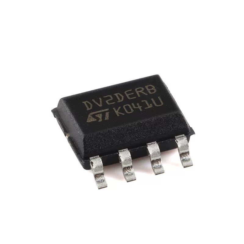
ST25DV04K-IER6S3 - 4Kbit Dynamic NFC/RFID Tag IC | STMicroelectronics
The ST25DV04K-IER6S3 is a dynamic NFC/RFID tag IC from STMicroelectronics, offering 4 Kbit of EEPROM memory with an I2C interface and an ISO 15693 / ISO 18000-3 Mode 1 compliant RF interface. It operates at 13.56 MHz and supports data rates up to 53 kbit/s in the RF interface, while the I2C interface supports up to 1 MHz. The device is housed in an SO-8 package (NXP-style) and is designed for applications requiring contactless data transfer and configuration, such as smart home devices, industrial equipment, and consumer electronics. Data verified as of 2026-08-05. What is a dynamic NFC/RFID tag IC? A dynamic NFC/RFID tag IC is a type of RFID transponder that combines a contactless RF interface with a wired interface (typically I2C) to allow a microcontroller to read and write the tag's memory both over the air and via the wired bus. This category sits within the broader hierarchy: NFC/RFID tag IC -> RFID transponder -> RFID/NFC integrated circuit -> wireless communication IC -> semiconductor. The dynamic nature means the tag can be updated in real time by the host MCU, enabling use cases like wireless configuration, data logging, and product authentication. Key features include 4 Kbit EEPROM organized in 128-byte pages, an I2C interface with a 1 MHz clock, an RF interface compliant with ISO 15693 and ISO 18000-3 Mode 1, a 64-bit unique identifier (UID), and an energy harvesting function that can power external circuits. The device supports a wide supply voltage range of 1.8V to 5.5V on the I2C side, and it includes an interrupt output to signal RF activity. The SO-8 package is compact and suitable for surface-mount assembly. Technically, the ST25DV04K-IER6S3 integrates an RF front-end with an analog-to-digital converter for energy harvesting, a state machine for protocol handling, and a memory controller for EEPROM access. The EEPROM is organized into 32 pages of 128 bits each, with a data retention of 10 years and an endurance of 1 million write cycles. The device supports both static and dynamic memory mapping, allowing the host to control which memory areas are accessible over RF. Typical applications include smart home devices (e.g., smart locks, thermostats), industrial equipment configuration, consumer electronics pairing (e.g., Bluetooth speakers, wearables), and medical device calibration. The energy harvesting feature enables battery-less operation for low-power sensors, and the I2C interface allows seamless integration with microcontrollers. When designing with this device, ensure proper antenna matching for the RF interface and place decoupling capacitors close to the VCC pin. The energy harvesting output should be buffered with a capacitor to provide stable power to external circuits. Also, consider the I2C address configuration via the RF field to avoid conflicts in multi-tag systems. This page synthesizes distributor pricing, drop-in alternatives, and practical design notes not found in the STMicroelectronics datasheet, providing a comprehensive resource for engineers evaluating the ST25DV04K-IER6S3.