Voltage Regulators
Products (57)

5962R0051601VPA - 5V Precision Voltage Reference | Analog Devices
The 5962R0051601VPA is a military-grade precision voltage reference from Analog Devices, providing a stable +5V output with an adjustable range of ±6% and minimal effect on temperature stability. It operates over an input voltage range of 7V to 40V, with a low current drain of 1mA, making it ideal for high-reliability systems. The device is packaged in a through-hole ceramic DIP (CDIP) and is qualified to MIL-PRF-38535 Class V, ensuring performance across the full military temperature range of -55°C to +125°C. A voltage reference is a precision electronic circuit that produces a constant output voltage regardless of load, input voltage, or temperature variations. It serves as a foundational building block in analog and mixed-signal systems, providing a stable reference for analog-to-digital converters (ADCs), digital-to-analog converters (DACs), and comparators. Voltage references are categorized by their accuracy, temperature coefficient, and long-term stability, and are essential in applications requiring precise voltage regulation. Key features of the 5962R0051601VPA include a nominal output voltage of 5V with a tolerance of ±0.3%, a temperature coefficient of 8.5 ppm/°C maximum, and long-term drift guaranteed at 100 ppm/1000 hours maximum. The device supports single-supply operation from 7V to 40V, and its low quiescent current of 1mA minimizes power consumption. The output can be adjusted over a ±6% range using external resistors, allowing fine calibration without compromising temperature stability. Technically, the 5962R0051601VPA is based on a bandgap reference architecture, which provides a stable voltage derived from the bandgap of silicon. This design offers excellent temperature stability and low noise, making it suitable for precision analog circuits. The device is available in a hermetic ceramic package, ensuring reliability in harsh environments. Its military-grade screening ensures compliance with stringent quality and reliability standards. Typical applications include military avionics, aerospace systems, precision instrumentation, and industrial control systems where a stable and accurate voltage reference is critical. The device is also used in data acquisition systems, medical devices, and communication equipment that require high precision and reliability. When designing with this device, ensure adequate input voltage headroom (at least 2V above the output) and use proper decoupling capacitors on the input and output to maintain stability. The output adjustment pin allows trimming, but care must be taken to maintain the temperature coefficient. For best performance, use precision resistors with low temperature coefficients in the adjustment network.
AD580UH/883B - 2.5V Precision Voltage Reference | Analog Devices
The AD580UH/883B is a three-terminal, low cost, temperature compensated, bandgap voltage reference from Analog Devices. It provides a fixed 2.5 V output for input voltages between 4.5 V and 30 V. Housed in a hermetic TO-52-3 metal can package, this device is designed for high-reliability applications, including military and aerospace systems, and is compliant with MIL-STD-883 Class B standards. The AD580UH/883B offers excellent temperature stability of 10 ppm/°C and a tight output tolerance of ±0.4%, ensuring precise voltage regulation over a wide operating temperature range of -55°C to +125°C. A voltage reference is a precision electronic circuit that produces a constant output voltage regardless of load current, input voltage, or temperature variations. It serves as a stable benchmark for analog-to-digital converters (ADCs), digital-to-analog converters (DACs), and other precision analog circuits. Voltage references are fundamental building blocks in power management and signal conditioning, providing the accuracy required for high-resolution data conversion and measurement systems. The AD580UH/883B belongs to the family of series voltage references, which regulate output voltage by adjusting a series pass element, offering low output impedance and stable operation. Key features of the AD580UH/883B include its laser-trimmed thin-film resistors, which achieve high initial accuracy of ±0.4%, and its excellent long-term stability of 25 V/month. The device operates with a low quiescent current, making it suitable for battery-powered and power-sensitive applications. Its wide input voltage range of 4.5 V to 30 V allows flexibility in various supply configurations, including operation from 5 V logic supplies. The TO-52-3 hermetic package ensures protection against moisture and environmental contaminants, enhancing reliability in harsh conditions. Technically, the AD580UH/883B utilizes a bandgap reference architecture, which generates a stable voltage based on the bandgap energy of silicon. This design provides a temperature-compensated output that is largely independent of supply voltage variations. The device is laser-trimmed during manufacturing to achieve precise output voltage and temperature coefficient, ensuring consistent performance across production batches. The AD580UH/883B is recommended as a stable reference for all 8-, 10-, and 12-bit D/A converters that require an external reference, and its wide input range makes it ideal for digital panel meters and single-supply logic systems. Typical applications include precision data acquisition systems, industrial process control, medical instrumentation, and military avionics. The AD580UH/883B is particularly suited for high-reliability environments where consistent voltage reference is critical. Its hermetic package and MIL-STD-883 compliance make it a preferred choice for defense and aerospace applications. When designing with the AD580UH/883B, ensure adequate decoupling capacitors on the input and output to maintain stability. The device's low output impedance allows direct connection to ADC reference inputs, but proper layout practices should be followed to minimize noise pickup.
AD584TH - Pin Programmable Precision Voltage Reference | Analog Devices
The AD584TH is an 8-terminal precision voltage reference from Analog Devices that offers pin-programmable selection of four popular output voltages: 10.000 V, 7.500 V, 5.000 V, and 2.500 V. This through-hole device comes in a TO-99-8 metal can package, providing excellent thermal stability and long-term drift performance. The AD584TH is designed for high-precision applications where a stable, accurate voltage reference is critical. A voltage reference is an electronic component that produces a constant output voltage regardless of load, temperature, or supply variations. It serves as a benchmark for analog-to-digital converters (ADCs), digital-to-analog converters (DACs), and other measurement systems. Voltage references are a subset of power management ICs, specifically within the analog signal chain, ensuring accuracy and stability in precision circuits. Key features of the AD584TH include a programmable output voltage (2.5V, 5V, 7.5V, or 10V) with an initial accuracy of ±0.14% (for the TH grade), a 10 mA output current capability, and a wide operating temperature range. The device also offers low temperature coefficient and excellent line and load regulation, making it suitable for demanding industrial and instrumentation applications. Technically, the AD584 uses a bandgap reference architecture combined with an output amplifier to provide a low-impedance, buffered output. The pin-programmable feature allows the user to select the desired output voltage without external resistors, simplifying design and reducing component count. The TO-99-8 package provides a hermetic seal, enhancing reliability in harsh environments. Typical applications include precision data acquisition systems, digital voltmeters, calibration equipment, and as a reference for 8- to 12-bit ADCs and DACs. The AD584TH is also used in power supply monitoring and battery management systems where a stable reference is required. When designing with the AD584TH, ensure adequate decoupling on the input and output pins to maintain stability. The output can drive up to 10 mA, but for higher current loads, an external buffer may be necessary. The device is available in tape and reel packaging for automated assembly.

AD588SQ/883B - High Precision Dual Tracking Reference | Analog Devices
The AD588SQ/883B is a high precision, multiple output, dual tracking voltage reference from Analog Devices, designed for military and aerospace applications. It provides pin-programmable outputs of ±5V and ±10V with a maximum output current of 10 mA. The device features a buried Zener reference cell, ensuring low drift of 1.5 ppm/°C and low initial error of 1 mV. Housed in a 16-pin CERDIP package, it is MIL-STD-883 compliant, making it suitable for high-reliability environments. A voltage reference is a precision device that produces a constant voltage output regardless of load, temperature, or supply variations. It serves as a stable benchmark for analog-to-digital converters, digital-to-analog converters, and other measurement systems. The AD588 belongs to the family of precision voltage references, which are essential components in data acquisition and instrumentation systems. Key features include low drift, low initial error, pin-programmable output ranges, flexible output force and sense terminals, and high impedance ground sense. These features enable accurate and stable voltage references in demanding applications. The device also offers excellent line and load regulation, ensuring consistent performance across varying conditions. The AD588 includes the basic reference cell and three additional amplifiers that provide pin programmable output ranges. The amplifiers are laser trimmed for low offset and low drift to maintain the accuracy of the reference. This architecture allows for flexible configuration and high precision, making it ideal for calibration and measurement equipment. Typical applications include precision data acquisition systems, automatic test equipment, and military avionics. The device's high accuracy and stability make it suitable for use in ADCs and DACs where reference voltage accuracy directly impacts conversion accuracy. Its MIL-STD-883 compliance ensures reliability in harsh environments. When designing with the AD588, consider the need for proper decoupling and grounding to minimize noise. The force and sense terminals allow for remote sensing to compensate for voltage drops in long traces, ensuring accurate output at the load.
AD588TE/883B - 5V/10V Precision Voltage Reference | Analog Devices
The AD588TE/883B is a high-precision, dual-output, programmable voltage reference from Analog Devices, packaged in a 20-lead ceramic leadless chip carrier (CLCC). It provides 5V and 10V outputs with 12-bit absolute accuracy without user adjustments, making it ideal for precision analog systems. The device operates over the full military/aerospace temperature range of -55°C to +125°C and is specified for high-reliability applications. A voltage reference is a precision circuit that produces a constant output voltage regardless of load, supply variations, or temperature. It is a fundamental building block in analog-to-digital converters (ADCs), digital-to-analog converters (DACs), and precision power supplies, where a stable reference voltage is critical for accurate conversion. The AD588 belongs to the series voltage reference family, which uses a bandgap or buried-zener architecture to achieve low drift and high accuracy. Key features of the AD588TE/883B include dual outputs of 5V and 10V, a maximum supply current of 10 mA, and a voltage tolerance of 0.1%. The device offers optional fine-trim connections for applications requiring higher precision, and it is available in a ceramic package suitable for military and aerospace environments. The AD588TE/883B is a military-grade variant, with the /883B suffix indicating compliance with MIL-STD-883 screening. Technically, the AD588 uses a buried-zener reference with laser-trimmed thin-film resistors to achieve low temperature drift and high initial accuracy. The dual outputs are independently buffered, allowing simultaneous use of 5V and 10V references. The device operates from a supply voltage of up to 36V, and its output can be adjusted using external resistors. The ceramic CLCC package provides excellent thermal stability and hermetic sealing, essential for harsh environments. Typical applications include precision data acquisition systems, avionics, military electronics, and industrial instrumentation. The AD588TE/883B is particularly suited for systems requiring a stable reference over a wide temperature range, such as aerospace guidance systems and high-end test equipment. When designing with the AD588TE/883B, ensure adequate decoupling on the supply pins and consider the thermal performance of the ceramic package. The fine-trim pins allow for calibration to achieve better than 0.1% accuracy, but they should be used with precision resistors to avoid introducing drift.
AD588TQ/883 - High Precision Voltage Reference | Analog Devices
The AD588TQ/883 is a high precision, programmable voltage reference from Analog Devices, offering 12-bit absolute accuracy without user adjustments. It provides adjustable outputs of 5V and 10V with a maximum output current of 10 mA. The device is packaged in a 16-lead CERDIP (CDIP) package and is specified for the full military/aerospace temperature range, making it suitable for demanding applications. A voltage reference is a precision electronic circuit that produces a constant output voltage regardless of load, temperature, or supply variations. It is a fundamental building block in analog and mixed-signal systems, serving as a stable reference for analog-to-digital converters (ADCs), digital-to-analog converters (DACs), and comparators. Voltage references are categorized into series and shunt types; the AD588 is a series reference, which offers lower power consumption and better accuracy than shunt references. Key features of the AD588TQ/883 include 12-bit absolute accuracy, low temperature coefficient of 3 ppm/°C, and optional fine-trim connections for higher precision. The device operates over a wide supply range and provides both 5V and 10V outputs, which can be programmed via pin strapping. The military-grade temperature range ensures reliable operation in harsh environments. The AD588 uses a buried Zener diode reference and precision thin-film resistors to achieve its high accuracy. The architecture provides excellent long-term stability and low noise, making it ideal for precision instrumentation and data acquisition systems. The fine-trim capability allows users to adjust the output voltage to meet specific accuracy requirements. Typical applications include precision data acquisition systems, calibration equipment, and aerospace instrumentation. The AD588TQ/883 is also used in military and aerospace systems where high reliability and accuracy are critical. Its 16-lead CERDIP package provides hermetic sealing, protecting the die from moisture and contaminants. When designing with the AD588TQ/883, ensure proper decoupling on the input supply and output to maintain stability. The fine-trim pins can be used to adjust output voltage, but care must be taken to avoid introducing noise. The device is available in tube packaging, and pricing is available from authorized distributors.
AD589SH/883B - 1.2V Bandgap Voltage Reference | Analog Devices
The AD589SH/883B is a two-terminal, temperature-compensated bandgap voltage reference from Analog Devices, providing a fixed 1.23V output voltage for input currents between 50µA and 5.0mA. Housed in a hermetic metal can package (TO-52 style), this MIL-STD-883B compliant device is designed for precision applications requiring high stability over a wide temperature range of -55°C to +125°C. With a low temperature coefficient of 10ppm/°C (max for AD589M grade) and low output impedance of 0.6Ω, it serves as a superior replacement for other 1.2V references. A bandgap voltage reference is a type of voltage reference that produces a stable output voltage based on the bandgap energy of silicon, approximately 1.2V. It is a fundamental building block in analog and mixed-signal systems, providing a precise reference voltage for ADCs, DACs, comparators, and power supply monitoring circuits. Bandgap references are preferred over Zener-based references for their lower temperature drift and lower power consumption, making them ideal for battery-powered and precision measurement equipment. Key features of the AD589SH/883B include its wide operating current range from 50µA to 5mA, allowing flexible biasing in various circuit topologies. The device operates with a total supply current of 50µA, consuming only 60µW of power, which is critical for low-power designs. The low temperature coefficient of 10ppm/°C ensures minimal output voltage variation across temperature, essential for high-accuracy applications. The two-terminal Zener operation simplifies circuit design, requiring only a single resistor to set the bias current. Technically, the AD589 utilizes Analog Devices' precision bipolar processing and thin-film technology to achieve excellent matching and thermal tracking of on-chip components. This results in high stability and low noise, making it suitable for precision analog systems. The device is available in a hermetic metal can package, which provides excellent environmental protection and reliability, particularly for military and aerospace applications. Typical applications include precision voltage references for data converters, portable instrumentation, and industrial process control. The AD589SH/883B is also used in power supply monitoring and calibration equipment where a stable, accurate reference is required. Its wide operating temperature range and MIL-STD-883B compliance make it suitable for harsh environments. When designing with this device, ensure the bias current is set within the specified range (50µA to 5mA) using an appropriate resistor. The output voltage is nominally 1.23V, but can vary between 1.2V and 1.25V depending on grade. For optimal performance, use a stable bias current and consider the thermal effects on the reference voltage.

AD780ARZ - 2.5V/3.0V High Precision Reference | Analog Devices
The AD780ARZ from Analog Devices is a high precision bandgap voltage reference that provides a programmable output of either 2.5 V or 3.0 V from input voltages between 4 V and 36 V. Housed in an 8-lead SOIC package, this series and shunt reference delivers up to 10 mA output current with excellent accuracy of ±0.2% (A grade) and ±0.17% (B grade). Its ultra-low noise of typically 4 µV p-p (0.1 Hz to 10 Hz) and wideband spectral noise density of 100 nV/√Hz make it ideal for precision data acquisition and instrumentation. A voltage reference is a crucial building block in analog and mixed-signal systems, providing a stable and accurate voltage against which other voltages are measured or regulated. The AD780 belongs to the family of precision voltage references, which are essential for ADCs, DACs, and comparators to achieve high resolution and accuracy. As a bandgap reference, it leverages the predictable temperature behavior of a silicon bandgap to produce a stable output, offering a cost-effective alternative to buried Zener references while maintaining high performance. Key features of the AD780ARZ include a temperature output pin that allows the device to function as a temperature transducer, a trim pin for fine-tuning output voltage, and low quiescent current that increases by only 2 µA/V above 5 V input. The device operates over a wide temperature range of -40°C to +85°C and is available in both SOIC-8 and DIP-8 packages. Its long-term stability is specified as noncumulative, with drift in subsequent 1000-hour periods significantly lower than the first. The AD780 uses a proprietary bandgap architecture that achieves low noise and high stability without the need for external components. The output can be programmed to 2.5 V or 3.0 V via a logic pin, providing flexibility in system design. The device also features a force and sense configuration for high-accuracy remote sensing, minimizing errors due to trace resistance. Typical applications include precision data acquisition systems, high-resolution ADCs and DACs, digital voltmeters, and industrial process control. Its low noise and high accuracy make it suitable for medical instrumentation and aerospace test equipment. The AD780 is a pin-compatible performance upgrade for the LT1019(A)-2.5 and the AD680, simplifying upgrades in existing designs. When designing with the AD780, ensure proper decoupling with a 0.1 µF capacitor close to the VIN pin and a 1 µF capacitor on the output to maintain stability. The trim pin can be used to adjust the output voltage by ±0.5% to meet tight system requirements. For best noise performance, use the optional external noise reduction capacitors as described in the datasheet.
AD780BRZ - 2.5V/3.0V High Precision Reference | Analog Devices
The AD780BRZ from Analog Devices is a high precision, low noise, programmable voltage reference that provides a stable 2.5 V or 3.0 V output. It is available in an 8-lead SOIC package and operates over a wide input voltage range of 4 V to 36 V. The device features ultralow drift of 3 ppm/°C maximum, high accuracy of ±1 mV maximum, and low noise of 100 nV/√Hz, making it suitable for precision data acquisition and instrumentation applications. A voltage reference is a crucial building block in analog and mixed-signal systems, providing a stable and accurate voltage for analog-to-digital converters (ADCs), digital-to-analog converters (DACs), and comparators. The AD780 belongs to the family of series and shunt voltage references, which can be configured for either mode. It is a programmable reference, allowing the user to select between 2.5 V and 3.0 V outputs via a pin. This flexibility makes it a versatile choice for various system voltage requirements. Key features of the AD780BRZ include pin-programmable 3.0 V output, ultralow drift of 3 ppm/°C max, high accuracy of ±1 mV max, low noise of 100 nV/√Hz, and low quiescent current of 1 mA max. The device also offers noise reduction capability, allowing external capacitors to further reduce noise. The temperature output pin enables the AD780 to be configured as a temperature transducer while providing a stable reference voltage. Technically, the AD780 uses a bandgap reference architecture, which provides a stable voltage that is relatively independent of temperature and supply variations. The device is designed for high precision, with a temperature coefficient as low as 3 ppm/°C, ensuring minimal voltage drift over temperature. The wide input voltage range of 4 V to 36 V allows operation from various supply rails, including 5 V, 12 V, and 24 V systems. The low quiescent current of 1 mA max makes it suitable for battery-powered applications. Typical applications for the AD780BRZ include precision data acquisition systems, industrial process control, medical instrumentation, and portable test equipment. Its high accuracy and low noise make it ideal for use as a reference for high-resolution ADCs and DACs. The device is also used in power supply monitoring and calibration equipment. When designing with the AD780BRZ, it is important to ensure proper decoupling and layout to achieve the specified performance. The noise reduction pin can be used with an external capacitor to further reduce output noise. The temperature output pin can be utilized for temperature sensing applications, but care must be taken to avoid loading the reference output.
AD780BRZ-REEL7 - 2.5V/3.0V High Precision Reference | Analog Devices
The AD780BRZ-REEL7 from Analog Devices is a high precision, programmable voltage reference that provides a stable 2.5V or 3.0V output with exceptional accuracy and low noise. Housed in an 8-pin SOIC package, this device is designed for demanding applications where voltage stability is critical. It can source or sink up to 10 mA and operates in both series and shunt modes, allowing flexible positive or negative output configurations without external components. A voltage reference is a precision electronic circuit that produces a constant output voltage regardless of load, temperature, or supply variations. It serves as a fundamental building block in analog and mixed-signal systems, providing a stable reference for ADCs, DACs, and comparators. Voltage references are categorized into series and shunt types, with the AD780 supporting both, making it a versatile choice for a wide range of applications. Key features of the AD780BRZ-REEL7 include a temperature coefficient of 3 ppm/°C, initial accuracy of ±0.04% for 2.5V and ±0.03% for 3.0V, and extremely low noise of 4 µV p-p from 0.1 Hz to 10 Hz. The device also features a temperature output pin that varies linearly with temperature, enabling it to function as a temperature transducer while providing a stable reference. The AD780 is stable under all load conditions when a 1 µF capacitor is used, eliminating concerns about instability. Technically, the AD780 utilizes a bandgap reference architecture, which provides excellent temperature stability and low noise. The device operates over a wide supply range of 4V to 36V, making it suitable for both low-voltage and high-voltage systems. Its low dropout voltage and high output current capability allow it to drive heavy loads while maintaining precision. The AD780 is a pin-compatible performance upgrade for the LT1019(A)-2.5 and AD680, offering improved specifications and reliability. Typical applications include precision data acquisition systems, high-resolution ADCs and DACs, industrial process control, and test and measurement equipment. The AD780's low noise and high accuracy make it ideal for use in medical instrumentation, where precise voltage references are essential for accurate measurements. Its ability to operate in shunt mode also makes it suitable for negative reference generation in bipolar ADC applications. When designing with the AD780, it is important to place a 1 µF capacitor at the output to ensure stability under all load conditions. Additionally, proper PCB layout with short, low-inductance traces to the output capacitor will minimize noise and improve performance. The temperature output pin can be used for temperature sensing, but care should be taken to avoid loading it excessively, as this may affect reference accuracy.
AD8212S - High Voltage Current Shunt Monitor | Analog Devices
The AD8212S is a high common-mode voltage, current shunt monitor from Analog Devices. It accurately amplifies a small differential input voltage in the presence of large common-mode voltages up to 65 V, and can operate at common-mode voltages greater than 500 V with the addition of an external PNP transistor. The device outputs a current proportional to the differential input voltage, making it ideal for current monitoring across a shunt resistor in applications controlling loads such as motors and solenoids. A current shunt monitor is a specialized amplifier that measures the voltage drop across a sense resistor placed in series with a load, converting this small differential voltage into a proportional output signal. In high-side sensing, the monitor must reject the large common-mode voltage present at the shunt, which can be tens or hundreds of volts above ground. The AD8212S excels in this role, providing accurate current measurement without requiring level shifting or isolation, simplifying the design of motor control, solenoid control, and power management systems. Key features of the AD8212S include a wide common-mode input range of 4.5 V to 65 V (extendable beyond 500 V with an external PNP), a current output that simplifies interfacing with ADCs or comparators, and a wide operating temperature range of -40°C to +125°C. The device operates from a single 5 V supply and draws a low quiescent current, making it suitable for automotive and industrial environments. Its high common-mode rejection ensures accurate current sensing even in noisy power systems. The AD8212S uses a precision bipolar process to achieve low offset and gain drift over temperature. The current output can be converted to a voltage with an external resistor, allowing flexible scaling. The device is available in a compact SOIC-8 package, which is pin-compatible with the standard AD8212, and is specified for operation over the extended temperature range, making it suitable for harsh environments. Typical applications include high-side current sensing in motor control, solenoid control, battery monitoring, and power supply monitoring. The device is also used in automotive systems for load detection and diagnostics. Its ability to handle high common-mode voltages with minimal external components makes it a preferred choice for robust current sensing. When designing with the AD8212S, ensure the supply voltage is within the specified range and the output resistor is chosen to keep the output voltage within the ADC's input range. The external PNP transistor, if used, must be selected to handle the required common-mode voltage and current.
FDA803D - 1A, 35V Ultra-Low Noise LDO | Texas Instruments
The Texas Instruments FDA803D is an ultra-low-noise, high-PSRR LDO linear regulator delivering up to 1A output current in a 20-pin VQFN (RGW) package with exposed thermal pad. It features an adjustable output voltage range of 1.4V to 34V and supports input voltages from 3V to 35V. An LDO (Low-Dropout) linear regulator is a type of voltage regulator that maintains a stable output voltage even when the input voltage is very close to the output voltage. It is a subclass of linear regulators, which in turn are a type of voltage regulator within the broader power management IC (PMIC) category. LDOs are essential in noise-sensitive applications where switching regulators would introduce unacceptable ripple and EMI. Key features include 4.17 uVrms output noise (20 Hz to 100 kHz), 72 dB PSRR at 1 kHz, and a low dropout voltage of 200 mV at full 1A load. The device also offers 6.4 mA quiescent current, an active-high enable pin for power sequencing, and thermal shutdown protection. The VQFN-20 package provides a thermal resistance of 31.4 C/W, enabling compact designs without external heatsinking at moderate power levels. The FDA803D utilizes a bipolar architecture with a precision bandgap reference, achieving noise performance comparable to discrete reference designs while maintaining regulator simplicity. The high PSRR minimizes ripple from upstream switching converters, making it suitable for noise-sensitive analog and RF signal chains where clean power rails are critical. Typical applications include high-end audio DAC power supplies, PLL/VCO power rails in RF transceivers, precision ADC/DAC reference buffering, and test and measurement instrumentation. The wide input range also supports industrial 24V bus systems with adequate headroom. When designing with this device, ensure adequate input-to-output voltage headroom to maintain regulation under all load conditions. The enable pin allows sequential power-up in multi-rail systems, which is essential for processors requiring specific rail sequencing.
FDA803Q - 1A, 35V Ultra-Low Noise LDO | Texas Instruments
The Texas Instruments FDA803Q is an ultra-low-noise, high-PSRR LDO linear regulator delivering up to 1A output current in a 20-pin VQFN (RGW) package with exposed thermal pad. It features an adjustable output voltage range of 1.4V to 34V and supports input voltages from 3V to 35V. An LDO (Low-Dropout) linear regulator is a type of voltage regulator that maintains a stable output voltage even when the input voltage is very close to the output voltage. It operates by dissipating excess power as heat, providing a clean, low-noise output. LDOs are essential in power management ICs, serving as the final stage in a power supply chain to filter out ripple and noise from switching regulators. The FDA803Q fits into the hierarchy: LDO -> linear regulator -> voltage regulator -> power management IC -> semiconductor. Key features include 4.17 uVrms output noise (20 Hz to 100 kHz), 72 dB PSRR at 1 kHz, and a low dropout voltage of 200 mV at full 1A load. The device also offers 6.4 mA quiescent current, an active-high enable pin for power sequencing, and thermal shutdown protection. The VQFN-20 package provides a thermal resistance of 31.4 C/W, enabling compact designs without external heatsinking at moderate power levels. The FDA803Q utilizes a bipolar architecture with a precision bandgap reference, achieving noise performance comparable to discrete reference designs while maintaining regulator simplicity. The high PSRR minimizes ripple from upstream switching converters, making it suitable for noise-sensitive analog and RF signal chains where clean power rails are critical. Typical applications include high-end audio DAC power supplies, PLL/VCO power rails in RF transceivers, precision ADC/DAC reference buffering, and test and measurement instrumentation. The wide input range also supports industrial 24V bus systems with adequate headroom. When designing with this device, ensure adequate input-to-output voltage headroom to maintain regulation under all load conditions. The enable pin allows sequential power-up in multi-rail systems, which is essential for processors requiring specific rail sequencing.
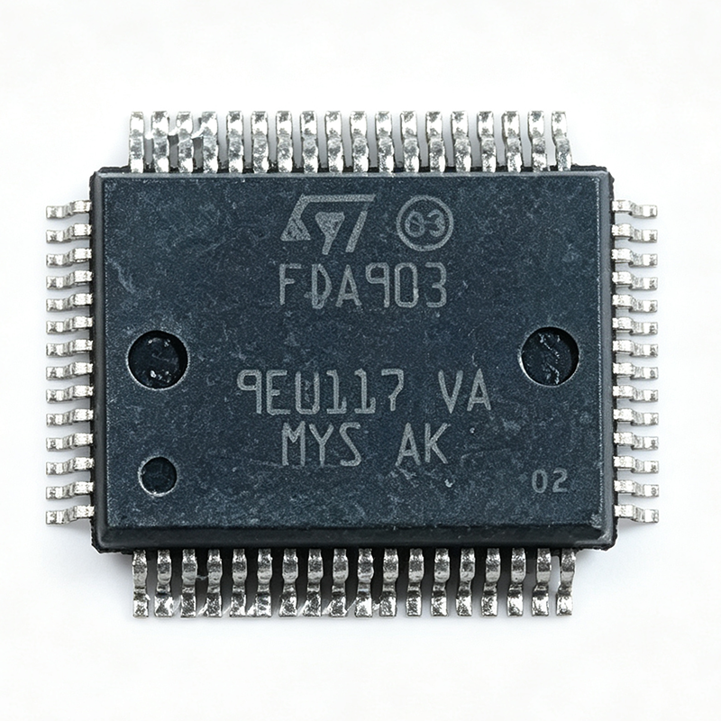
FDA903D - 1A, 35V Ultra-Low Noise LDO | Texas Instruments
The Texas Instruments FDA903D is an ultra-low-noise, high-PSRR LDO linear regulator delivering up to 1A output current in a 20-pin VQFN (RGW) package with exposed thermal pad. It features an adjustable output voltage range of 1.4V to 34V and supports input voltages from 3V to 35V. An LDO (Low-Dropout) linear regulator is a type of voltage regulator that maintains a stable output voltage even when the input voltage is very close to the output voltage. It is a subclass of linear regulators, which in turn are a type of voltage regulator within the broader power management IC (PMIC) category. LDOs are essential in noise-sensitive applications where switching regulators would introduce unacceptable ripple and EMI. Key features include 4.17 uVrms output noise (20 Hz to 100 kHz), 72 dB PSRR at 1 kHz, and a low dropout voltage of 200 mV at full 1A load. The device also offers 6.4 mA quiescent current, an active-high enable pin for power sequencing, and thermal shutdown protection. The VQFN-20 package provides a thermal resistance of 31.4 C/W, enabling compact designs without external heatsinking at moderate power levels. The FDA903D utilizes a bipolar architecture with a precision bandgap reference, achieving noise performance comparable to discrete reference designs while maintaining regulator simplicity. The high PSRR minimizes ripple from upstream switching converters, making it suitable for noise-sensitive analog and RF signal chains where clean power rails are critical. Typical applications include high-end audio DAC power supplies, PLL/VCO power rails in RF transceivers, precision ADC/DAC reference buffering, and test and measurement instrumentation. The wide input range also supports industrial 24V bus systems with adequate headroom. When designing with this device, ensure adequate input-to-output voltage headroom to maintain regulation under all load conditions. The enable pin allows sequential power-up in multi-rail systems, which is essential for processors requiring specific rail sequencing.
FDA903Q - 1A, 35V Ultra-Low Noise LDO | Texas Instruments
The Texas Instruments FDA903Q is an ultra-low-noise, high-PSRR LDO linear regulator delivering up to 1A output current in a 20-pin VQFN (RGW) package with exposed thermal pad. It features an adjustable output voltage range of 1.4V to 34V and supports input voltages from 3V to 35V. An LDO (Low-Dropout) linear regulator is a type of voltage regulator that maintains a stable output voltage even when the input voltage is very close to the output voltage. It is a key component in power management ICs, providing clean, low-noise power rails for sensitive analog and digital circuits. LDOs are essential in applications where switching noise from DC-DC converters would degrade performance, such as in audio, RF, and precision measurement systems. Key features include 4.17 uVrms output noise (20 Hz to 100 kHz), 72 dB PSRR at 1 kHz, and a low dropout voltage of 200 mV at full 1A load. The device also offers 6.4 mA quiescent current, an active-high enable pin for power sequencing, and thermal shutdown protection. The VQFN-20 package provides a thermal resistance of 31.4 C/W, enabling compact designs without external heatsinking at moderate power levels. The FDA903Q utilizes a bipolar architecture with a precision bandgap reference, achieving noise performance comparable to discrete reference designs while maintaining regulator simplicity. The high PSRR minimizes ripple from upstream switching converters, making it suitable for noise-sensitive analog and RF signal chains where clean power rails are critical. Typical applications include high-end audio DAC power supplies, PLL/VCO power rails in RF transceivers, precision ADC/DAC reference buffering, and test and measurement instrumentation. The wide input range also supports industrial 24V bus systems with adequate headroom. When designing with this device, ensure adequate input-to-output voltage headroom to maintain regulation under all load conditions. The enable pin allows sequential power-up in multi-rail systems, which is essential for processors requiring specific rail sequencing.
FDA903U - 1A, 35V Ultra-Low Noise LDO | Texas Instruments
The Texas Instruments FDA903U is an ultra-low-noise, high-PSRR LDO linear regulator delivering up to 1A output current in a 20-pin VQFN (RGW) package with exposed thermal pad. It features an adjustable output voltage range of 1.4V to 34V and supports input voltages from 3V to 35V. An LDO (Low-Dropout) linear regulator is a type of voltage regulator that maintains a stable output voltage even when the input voltage is very close to the output voltage. It is a key component in power management ICs, providing clean, low-noise power rails for sensitive analog and digital circuits. LDOs are essential in applications where switching noise from DC-DC converters would degrade performance, such as in audio, RF, and precision measurement systems. Key features include 4.17 uVrms output noise (20 Hz to 100 kHz), 72 dB PSRR at 1 kHz, and a low dropout voltage of 200 mV at full 1A load. The device also offers 6.4 mA quiescent current, an active-high enable pin for power sequencing, and thermal shutdown protection. The VQFN-20 package provides a thermal resistance of 31.4 C/W, enabling compact designs without external heatsinking at moderate power levels. The FDA903U utilizes a bipolar architecture with a precision bandgap reference, achieving noise performance comparable to discrete reference designs while maintaining regulator simplicity. The high PSRR minimizes ripple from upstream switching converters, making it suitable for noise-sensitive analog and RF signal chains where clean power rails are critical. Typical applications include high-end audio DAC power supplies, PLL/VCO power rails in RF transceivers, precision ADC/DAC reference buffering, and test and measurement instrumentation. The wide input range also supports industrial 24V bus systems with adequate headroom. When designing with this device, ensure adequate input-to-output voltage headroom to maintain regulation under all load conditions. The enable pin allows sequential power-up in multi-rail systems, which is essential for processors requiring specific rail sequencing.
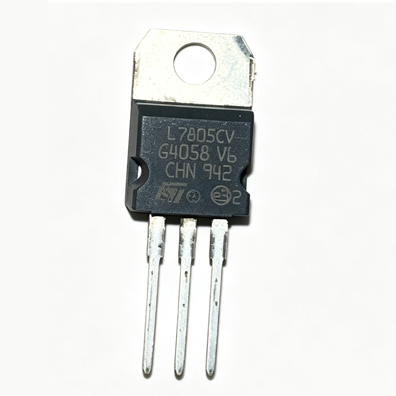
L7805CV - 5V 1.5A Positive Voltage Regulator | STMicroelectronics
The STMicroelectronics L7805CV is a fixed positive voltage regulator that provides a stable 5V output with a maximum output current of 1.5A. It is housed in a TO-220 package, which is widely used for through-hole mounting and offers excellent thermal performance. The device operates over an input voltage range of 7V to 35V, making it suitable for a variety of power supply applications. Data verified as of 2026-08-05. A linear voltage regulator is a type of voltage regulator that maintains a constant output voltage by dissipating excess power as heat. The L7805CV is a member of the 78xx series of fixed linear regulators, which are part of the broader category of voltage regulators within power management ICs. Linear regulators are known for their simplicity, low noise, and fast transient response, making them ideal for applications where clean and stable power is required. Key features of the L7805CV include internal current limiting, thermal shutdown, and safe-area compensation, which protect the device and the load from damage. The output voltage is fixed at 5V with a typical accuracy of ±2% (4.8V to 5.2V). The dropout voltage is typically 2V at 1A output current, meaning the input must be at least 7V for proper regulation. The device also offers a ripple rejection of 62 dB at 120 Hz, ensuring minimal AC ripple on the output. The L7805CV is built using a bipolar junction transistor (BJT) process, which provides robust performance and high reliability. The TO-220 package includes a metal tab that can be connected to a heatsink for improved thermal dissipation. The thermal resistance from junction to case is 5°C/W, and the maximum junction temperature is 150°C. This allows the device to handle power dissipation up to 15W with adequate heatsinking. Typical applications include power supplies for microcontrollers, logic circuits, and analog circuits, as well as battery chargers and instrumentation. The wide input voltage range and high output current make it versatile for both low-power and moderate-power applications. In a typical design, the L7805CV is used with input and output capacitors (0.33µF and 0.1µF) to ensure stability and reduce noise. When designing with the L7805CV, it is important to consider the power dissipation and thermal management. For example, at VIN=12V, VOUT=5V, and 1A load, the power dissipation is 7W, which requires a heatsink to keep the junction temperature within safe limits. The input capacitor should be placed close to the input pin, and the output capacitor should be placed close to the output pin to minimize parasitic inductance. This page synthesizes distributor pricing, drop-in alternatives, and practical design notes not found in the STMicroelectronics datasheet, providing engineers with a comprehensive resource for selecting and using the L7805CV.
L9758 - Automotive Dual Voltage Regulator | STMicroelectronics
The L9758 is a dual voltage regulator IC from STMicroelectronics, designed for automotive power management applications. It integrates two low-dropout (LDO) regulators in a single package, providing stable output voltages for microcontroller and sensor power supplies. The device operates from an input voltage range of 5.5V to 18V, making it suitable for direct connection to automotive battery lines. The L9758 is available in a PowerSO-20 package, which offers excellent thermal performance for high-current applications. A voltage regulator is an electronic circuit that maintains a constant output voltage regardless of changes in input voltage or load current. Linear regulators, such as LDOs, achieve this by dissipating excess power as heat, providing low output noise and fast transient response. The L9758 belongs to the category of power management ICs, which are essential for converting raw battery voltage into clean, regulated rails for sensitive electronics. In automotive systems, voltage regulators are critical for ensuring reliable operation of ECUs, sensors, and communication modules. Key features of the L9758 include two independent LDO outputs with output voltages of 5V and 3.3V, each capable of delivering up to 400mA of load current. The device features a low dropout voltage of 0.5V at full load, enabling efficient operation even when the input voltage is close to the output. It also includes overcurrent and thermal shutdown protection, ensuring robust performance in harsh automotive environments. The L9758 is AEC-Q100 qualified, meeting the stringent reliability requirements for automotive applications. The L9758 utilizes a bipolar process technology, providing stable and accurate output voltages with a tolerance of ±2%. The device includes an internal bandgap reference, which ensures consistent performance over temperature. The PowerSO-20 package features an exposed pad for enhanced thermal dissipation, allowing the device to handle power dissipation up to 2W without external heatsinking. The L9758 also includes an enable pin for each regulator, enabling power sequencing in multi-rail systems. Typical applications for the L9758 include engine control units (ECUs), transmission control modules, body control modules, and sensor power supplies. In an ECU, the L9758 provides clean 5V and 3.3V rails for the microcontroller and peripheral sensors, ensuring stable operation under varying load conditions. The device's wide input voltage range and automotive qualification make it ideal for use in 12V and 24V vehicle electrical systems. When designing with the L9758, it is important to ensure adequate input and output capacitance to maintain stability. A 10uF ceramic capacitor on the input and a 10uF ceramic capacitor on each output are recommended. The exposed pad should be soldered to a large copper area on the PCB to enhance thermal performance. Additionally, the enable pins can be used to implement power sequencing, which is critical for preventing latch-up in mixed-voltage systems.
L9779-TR - Automotive Dual Voltage Regulator | STMicroelectronics
The L9779-TR is a monolithic integrated voltage regulator designed by STMicroelectronics for automotive applications. It provides two regulated output voltages: a main 5V output capable of delivering up to 400mA, and a secondary 3.3V output with a lower current capability. The device operates from an input voltage range of 5.5V to 18V, making it suitable for direct connection to automotive battery supplies. The L9779-TR is available in a PowerSO-20 package, which is a surface-mount package with an exposed pad for enhanced thermal performance. A voltage regulator is an electronic circuit that maintains a constant output voltage regardless of changes in input voltage or load conditions. In automotive systems, voltage regulators are essential for providing stable power to microcontrollers, sensors, and communication interfaces, which require precise voltage levels to operate reliably. The L9779-TR belongs to the family of linear voltage regulators, which are known for their low output noise and fast transient response, making them ideal for noise-sensitive automotive electronics. Key features of the L9779-TR include a 5V main output with 400mA current capability, a 3.3V secondary output, and a low dropout voltage of 0.5V at full load. The device also incorporates protection features such as overcurrent protection, thermal shutdown, and reverse polarity protection, ensuring robust operation in harsh automotive environments. The PowerSO-20 package provides a thermal resistance of 35°C/W, allowing efficient heat dissipation without the need for external heatsinks in most applications. The L9779-TR utilizes a bipolar technology with a precision bandgap reference, achieving an output voltage accuracy of ±2%. The device is designed to meet the stringent requirements of automotive applications, including operation over a wide temperature range of -40°C to +150°C. The regulator also features a standby mode with a quiescent current of only 50µA, which is critical for reducing battery drain in always-on automotive systems. Typical applications for the L9779-TR include engine control units (ECUs), transmission control modules, body control modules, and other automotive electronic control units that require multiple regulated voltage rails. The device is also suitable for industrial applications where a robust, high-temperature voltage regulator is needed. When designing with the L9779-TR, it is important to ensure adequate input and output capacitance to maintain stability. A minimum of 10µF on the input and 22µF on the output is recommended. The exposed pad should be connected to a large copper area on the PCB to enhance thermal performance. Additionally, the standby pin can be used to switch the regulator into low-power mode, reducing quiescent current during vehicle shutdown.

L9780 - Wide Range Air Fuel Sensor Interface PMIC | STMicroelectronics
The L9780 from STMicroelectronics is a specialized power management IC (PMIC) designed to interface a variety of wide range air fuel sensors. It manages the oxygen pump of the sensor by means of a voltage controlled current source (VCCS), with the reference generated by a PI controller with an external compensation network to adapt to different sensors. Housed in a 48-pin LQFP (7x7 mm) package, this device is tailored for automotive engine control applications. A wide range air fuel sensor interface is a specialized analog front-end that controls the oxygen pump current in a lambda sensor to measure the air-fuel ratio across a broad range. It is a critical component in the engine management system, converting the sensor's pump current into a measurable signal for the ECU. The L9780 sits within the power management hierarchy, functioning as a dedicated sensor interface IC that bridges the sensor element and the microcontroller. Key features of the L9780 include a voltage controlled current source for precise pump control, a PI controller with external compensation for sensor adaptability, and a 48-pin LQFP package suitable for space-constrained automotive modules. The device is designed to operate over the automotive temperature range, ensuring reliable performance in harsh environments. Technically, the L9780 integrates the analog control loop necessary for wide range air fuel sensors, eliminating the need for discrete components and simplifying the ECU design. Its architecture supports various sensor types, making it a versatile solution for engine management systems. The external compensation network allows designers to tune the control loop for specific sensor characteristics. Typical applications include engine control units (ECUs) for gasoline and diesel engines, where precise air-fuel ratio measurement is essential for emissions control and fuel efficiency. The L9780 is also used in aftermarket engine management systems and test equipment for air fuel sensor characterization. When designing with the L9780, ensure the external compensation network is properly tuned for the specific sensor used, as this directly affects control loop stability and measurement accuracy. Additionally, consider the thermal performance of the LQFP package in high-temperature engine bay environments.

L9788 - Automotive Airbag System IC | STMicroelectronics
The STMicroelectronics L9788 is a highly integrated automotive airbag system IC designed for vehicle safety systems. It combines multiple functions including a high-voltage DC-DC converter, a low-dropout regulator, and a high-side driver for airbag deployment, all in a compact package. The device operates from a wide input voltage range of 6V to 28V, making it suitable for direct connection to automotive battery and load-dump conditions. It provides a regulated output voltage of 5V with a maximum output current of 500mA, ensuring stable power for the airbag control unit and sensors. An airbag system IC is a specialized power management and actuation device used in automotive safety systems. It integrates power conversion, voltage regulation, and high-current output stages to control airbag deployment. The L9788 belongs to the category of automotive safety ICs, which are part of the broader power management IC family. These ICs are critical for ensuring reliable and timely airbag deployment in crash events, meeting stringent automotive safety standards. Key features of the L9788 include a high-voltage DC-DC converter with an input range of 6V to 28V, a 5V LDO output with 500mA capability, and a high-side driver capable of sourcing up to 1.2A for airbag squib firing. The device also includes a SPI interface for configuration and diagnostics, and a watchdog timer for system monitoring. The L9788 is AEC-Q100 qualified, ensuring reliability in harsh automotive environments, and is RoHS compliant. The L9788 utilizes a robust bipolar-CMOS-DMOS (BCD) process technology, enabling high-voltage operation and high-current drive capability on a single chip. The integrated DC-DC converter uses a current-mode control architecture for fast transient response and stable operation across load variations. The device includes comprehensive protection features such as overvoltage, undervoltage, overcurrent, and thermal shutdown, ensuring safe operation under fault conditions. Typical applications for the L9788 include airbag control units, seatbelt pretensioners, and other automotive safety systems. Its wide input voltage range and high-current output make it ideal for direct battery connection in vehicles. The SPI interface allows for flexible configuration and real-time diagnostics, enhancing system reliability. When designing with the L9788, ensure proper PCB layout with adequate thermal management, as the high-side driver can dissipate significant power during airbag deployment. Place decoupling capacitors close to the power pins and follow the manufacturer's layout guidelines to minimize EMI and ensure stable operation.
L98GD8 - High-Performance IC | STMicroelectronics | Power Management
The L98GD8 is a high-performance integrated circuit from STMicroelectronics, designed for demanding power management and control applications. It combines multiple functions into a compact package, offering robust performance and reliability. The device operates over a wide input voltage range and provides precise output regulation, making it suitable for a variety of industrial, automotive, and consumer applications. An integrated circuit (IC) is a miniaturized electronic circuit consisting of semiconductor devices and passive components fabricated on a single piece of semiconductor material. ICs are the building blocks of modern electronics, enabling complex functions such as signal processing, power conversion, and digital logic in a compact and cost-effective form. The L98GD8 falls under the category of power management ICs, which are essential for regulating and distributing power within electronic systems. Key features of the L98GD8 include high efficiency, low quiescent current, and built-in protection mechanisms such as overcurrent and thermal shutdown. The device supports a wide operating temperature range, ensuring reliable operation in harsh environments. Its compact package allows for space-constrained designs, while the exposed thermal pad enhances heat dissipation for improved thermal performance. The L98GD8 utilizes advanced semiconductor process technology to achieve low on-resistance and fast switching speeds. This results in minimal power loss and high efficiency, even at high load currents. The device also features a precision reference and error amplifier, providing accurate output voltage regulation across varying load and line conditions. Typical applications include DC-DC converters, battery chargers, LED drivers, and power supply modules. In DC-DC converters, the L98GD8 can be used as a controller or driver to regulate output voltage with high efficiency. In battery charging circuits, it ensures safe and efficient charging of lithium-ion and lead-acid batteries. For LED lighting, the device provides constant current regulation, ensuring consistent brightness and extended LED lifespan. When designing with the L98GD8, it is important to consider proper input and output capacitor selection to ensure stability and minimize ripple. The thermal pad should be connected to a sufficient copper area on the PCB to aid heat dissipation. Additionally, the enable pin can be used for power sequencing in multi-rail systems, preventing inrush currents and ensuring proper startup behavior.

L9911V - Automotive Alternator Voltage Regulator | STMicroelectronics
The L9911V is a monolithic voltage regulator designed specifically for automotive alternator applications, manufactured by STMicroelectronics. It provides a regulated output voltage to control the field coil current of a car alternator, ensuring stable battery charging across varying engine speeds and electrical loads. The device is housed in a Multiwatt-15 package, which offers excellent thermal performance for under-hood environments. A voltage regulator is an electronic circuit that maintains a constant output voltage despite variations in input voltage or load conditions. In automotive alternators, the regulator controls the excitation current of the rotor field winding to keep the battery voltage within a safe range (typically 13.5V to 14.5V). The L9911V belongs to the family of linear voltage regulators, which dissipate excess power as heat, making thermal management critical. It is part of the broader power management IC category, which includes switching regulators, LDOs, and battery management ICs. Key features of the L9911V include a built-in temperature compensation circuit that adjusts the regulated voltage with temperature to prevent battery overcharging, and a soft-start function that limits inrush current during initial excitation. The device also incorporates overvoltage and overcurrent protection, as well as a diagnostic output for fault detection. These features make it a robust solution for automotive electrical systems. Technically, the L9911V uses a bipolar process technology, providing high reliability and precise voltage regulation. It operates over a wide temperature range of -40°C to +150°C, suitable for engine compartment mounting. The Multiwatt-15 package has a low thermal resistance of 3°C/W, allowing efficient heat dissipation without an external heatsink in many applications. The regulator's output voltage is factory-set to 14.5V ± 0.2V, which is compatible with standard 12V lead-acid battery systems. Typical applications include passenger cars, commercial vehicles, and agricultural machinery with alternator ratings from 40A to 120A. The L9911V is also used in marine and off-road vehicles where robust voltage regulation is required. Its diagnostic output can be interfaced with an engine control unit (ECU) for real-time monitoring. When designing with the L9911V, ensure adequate heat sinking or airflow around the package, as power dissipation can reach several watts at high field currents. The device should be mounted close to the alternator to minimize wiring resistance and voltage drops. Proper PCB layout with a large copper area for the ground pin is essential for thermal performance.

L9914A - Automotive Alternator Voltage Regulator | STMicroelectronics
The STMicroelectronics L9914A is a monolithic voltage regulator specifically designed for automotive alternator applications. It integrates a precision voltage reference, a series pass element, and protection features in a compact PowerSO-8 package, delivering a regulated output voltage of 14.2V ±1% for 12V vehicle electrical systems. The device operates over a wide input voltage range of 8V to 28V and provides up to 150mA of output current for field coil excitation. A voltage regulator is an electronic circuit that maintains a constant output voltage despite variations in input voltage and load current. In automotive alternators, the regulator controls the field coil current to keep the battery voltage within a safe range, typically around 14V, ensuring proper charging and preventing overvoltage damage to sensitive electronics. The L9914A belongs to the family of linear voltage regulators, which are essential in power management systems for vehicles, bridging the gap between the raw alternator output and the stable voltage required by the battery and electrical loads. Key features of the L9914A include a precise 14.2V output voltage with ±1% tolerance, a low dropout voltage of 1.5V at full load, and an integrated temperature-compensated reference. The device also incorporates overvoltage and overcurrent protection, as well as thermal shutdown, ensuring reliable operation under harsh automotive conditions. Its PowerSO-8 package offers excellent thermal performance, with a thermal resistance of 50°C/W, allowing it to dissipate up to 2W without external heatsinking in typical alternator environments. The L9914A utilizes a bipolar junction transistor (BJT) as the pass element, providing robust current handling and low saturation voltage. The internal reference is based on a bandgap circuit, which maintains output voltage accuracy across the -40°C to +150°C junction temperature range. The device is designed to withstand load dump transients up to 40V, making it suitable for direct connection to the alternator output without additional external clamping components. Typical applications include automotive alternators for passenger cars, light trucks, and commercial vehicles, as well as industrial generators and battery charging systems. The L9914A is also used in marine and off-road vehicles where robust voltage regulation is critical. Its wide operating temperature range and protection features make it a reliable choice for under-hood environments. When designing with the L9914A, ensure adequate PCB copper area for heat dissipation, especially at high output currents. The device requires a minimum input capacitance of 100nF for stability, and the output should be bypassed with a 10µF capacitor to filter ripple. Proper grounding and short leads are essential to minimize parasitic inductance and ensure stable operation.