The Texas Instruments ISO6763DWR is a general-purpose six-channel (3-forward/3-reverse) reinforced digital isolator that transfers digital signals across a SiO2 capacitive isolation barrier at up to 50 Mbps with a 5000 VRMS isolation rating. Key verified specifications include a 1500 VRMS working voltage, up to 10 kV surge withstand, 50 kV/us minimum common-mode transient immunity (up to 150 kV/us typical per the ISO676x datasheet), a dual-supply architecture of 1.71 V to 1.89 V on side 1 and 2.25 V to 5.5 V on side 2 with direct 1.8 V logic support, and -40C to +125C operation in a 16-pin SOIC (DW, 7.50 mm width) surface-mount package. The part is active in lifecycle status and in stock at XAIPART with 99,999 units available, priced from $2.95 at single-unit quantities down to $1.85 at 1000 units as of 2026-09-05, with MOQ 1. It supports isolated CAN, RS-232, RS-485, and SPI links and is qualified for industrial and automotive-adjacent designs (an AEC-Q100 Q1 variant, the ISO6763QDWRQ1, shares the same footprint).
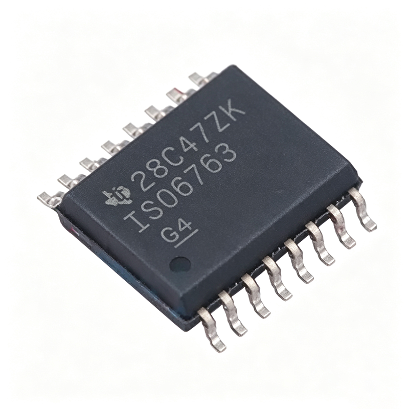
What Is the ISO6763DWR and Why Do Designers Choose It?
The ISO6763DWR belongs to the class of reinforced digital isolators: semiconductor devices that move logic signals across a galvanic barrier without any conductive connection, replacing optocouplers in industrial interfaces and power-management systems. TI constructs the barrier with silicon dioxide (SiO2) capacitive isolation, a dielectric that delivers long barrier lifetime at the device's 1500 VRMS working voltage and robust EMC performance against common-mode transients.
The symmetrical 3-forward/3-reverse channel configuration is the defining architectural choice. Six independent channels in one 16-pin SOIC let a single package isolate a full bidirectional bus — for example, a full-duplex RS-485 link with TX, RX, and direction control, or an isolated SPI link with SCLK, MOSI, MISO, and chip-select plus an interrupt or status line in the reverse direction. Where an optocoupler-based design would need six discrete optocouplers plus their bias resistors, the ISO6763DWR integrates everything into one surface-mount footprint, reducing BOM count, board area, and the aging-related degradation inherent to LED-based optocouplers.
Another differentiator is speed. Optocouplers typically struggle to reach the multi-megabit range, while the ISO6763DWR sustains 50 Mbps across the barrier — far beyond RS-485's conventional 10 Mbps ceiling and RS-232's 115.2 kbps standard rate, and sufficient for high-throughput SPI to fast data converters and FPGA configuration links.
How Do You Select and Design In the ISO6763DWR?
Selection starts with three verified parameters. First, confirm the isolation class: the 5000 VRMS reinforced isolation rating and 1500 VRMS working voltage address reinforced-insulation system requirements for industrial safety isolation. Second, confirm the speed budget: 50 Mbps maximum data rate with 50 kV/us minimum CMTI (up to 150 kV/us typical). Third, confirm the supply architecture: side 1 requires a narrow 1.71 V to 1.89 V domain for 1.8 V logic, while side 2 accepts 2.25 V to 5.5 V for 3.3 V or 5 V logic — no level-shift circuitry needed between mismatched logic domains.
For power supply design, TI's guidance is explicit: bypass both VCC pins with 0.1 uF and 1 uF ceramic capacitors placed as close to the package as possible. Designers must also verify that the logic-side supply domain matches the narrow 1.71 V to 1.89 V range of the low-voltage side — a regulated 1.8 V rail is required, and a 1.8 V rail that drifts outside this window will violate the datasheet operating conditions.
For signal integrity, budget the per-channel propagation delay and channel-to-channel skew when running SPI at the maximum clock rate, so setup and hold margins remain positive at the receiving device. For fieldbus designs on motor drives or inverter-heavy environments, the high CMTI is the parameter that matters most: steep dv/dt events such as IGBT switching transients will not corrupt data crossing the barrier.
Channel mapping tips: the 3/3 split maps directly to RS-485's TX, RX, and transceiver direction-control signals; to CAN's TX, RX, standby, and fault-flag signaling between controller and an isolated transceiver; and to RS-232's TXD, RXD, and handshake pairs (RTS/CTS, DTR/DSR) in both directions.
Package and temperature: the 16-SOIC DW body measures 0.295 in (7.50 mm) wide and the device operates from -40C to +125C, covering industrial cabinets and automotive under-hood and battery-pack environments. For automotive production programs requiring AEC-Q100 components, use the pin-compatible ISO6763QDWRQ1 (or ISO6763FQDWRQ1 for the F default-output option) so one PCB layout serves both industrial and automotive builds.
ISO6763DWR vs the Alternatives: Which Part Should You Use?
Based on verified cross-reference data, no cross-brand part (Skyworks, Broadcom, NVE, Renesas) was confirmed as a pin-to-pin drop-in equivalent for the ISO6763DWR in the 16-SOIC DW package; competing digital isolators use different pin maps that require PCB modification. The safest replacements are TI's own pin-compatible family members:
| Parameter | ISO6763DWR | ISO7763DWR | ISO6763FDWR | ISO6763QDWRQ1 |
|---|---|---|---|---|
| Generation / positioning | Current-generation general-purpose | Previous-generation equivalent | F default-output variant family | Automotive-qualified (AEC-Q100, Q1) |
| Channel configuration | 6 (3 forward / 3 reverse) | 3/3 channels (same) | 3/3 channels (same) | Pin-compatible with ISO6763DWR |
| Maximum data rate | 50 Mbps | 50 Mbps | 50 Mbps | [DATA_NEEDED: maximum data rate] |
| Package | 16-SOIC (DW), 7.50 mm width | Same 16-SOIC (DW) package | Same 16-SOIC (DW) package | Same 16-SOIC (DW) package |
| Isolation rating | 5000 VRMS reinforced | [DATA_NEEDED: isolation rating] | 5000 VRMS reinforced | [DATA_NEEDED: isolation rating] |
| Drop-in compatible? | — | Yes, pin-to-pin per TI alternate-product listing | Same footprint, PCB reuse without redesign | Yes, BOM substitution on same layout |
| Best for | New designs; newest barrier technology and EMC robustness | Cost-driven or existing-design continuity | Fail-safe requirements needing F default-output behavior | Automotive builds requiring AEC-Q100 |
Practical guidance: choose ISO6763DWR for new designs to get the newest barrier technology and EMC robustness; choose ISO7763DWR for cost-driven programs or continuity of existing designs. When choosing between ISO6763DWR and ISO6763FDWR, consult the ISO676x datasheet's feature comparison table, because the F suffix changes default output states and default-output timing behavior — the correct choice depends on your fail-safe requirements. Before finalizing any substitution, verify supply-range and default-output details against the replacement part's datasheet.
What Are the Proven Application Circuits for the ISO6763DWR?
Verified applications from the product database include isolated RS-485 fieldbus nodes, isolated CAN bus interfaces, isolated SPI communication, battery management systems, PLC I/O module isolation, and RS-232 legacy equipment isolation. A representative production-grade design is the isolated RS-485 node:
Design example — isolated full-duplex RS-485 fieldbus node. The problem: a microcontroller in a grounded control cabinet must communicate with field transceivers sitting at different ground potentials, with industrial safety isolation and immunity to large ground-potential differences. The approach: place the ISO6763DWR between the MCU and an RS-485 transceiver such as TI's THVD1550. Three forward channels carry TX and direction-control signals; three reverse channels carry RX and fault/status signals. Power side 1 from a regulated 1.8 V rail (within 1.71 V to 1.89 V) and side 2 at 3.3 V or 5 V to match the transceiver within the 2.25 V to 5.5 V range. Bypass both VCC pins with 0.1 uF and 1 uF ceramics placed as close to the package as possible. The margin math is straightforward: the isolator's 50 Mbps ceiling comfortably exceeds RS-485's conventional 10 Mbps maximum, so propagation delay consumes only a small fraction of the bit period, and the 50 kV/us minimum CMTI prevents corruption from ground-potential steps between field nodes and cabinets. The 5000 VRMS reinforced barrier satisfies industrial safety isolation requirements. Result: a single 16-pin SOIC replaces six discrete optocoupler channels and their bias components, cutting BOM count and board area while eliminating LED aging as a failure mechanism.
Battery management note. In EV and energy-storage BMS designs, the ISO6763DWR isolates SPI or UART between the low-voltage controller domain and the high-voltage stack-monitoring domain. The 5000 VRMS reinforced isolation and 1500 VRMS working voltage form the safety barrier between pack-level potentials (hundreds of volts) and the system controller, and 1.8 V logic support interfaces directly with low-power MCUs. Pairing the isolator with TI's BQ76952 battery monitor on the stack side creates a complete isolated measurement and communication chain; use the ISO6763QDWRQ1 for automotive production requiring AEC-Q100.
What Is the ISO6763DWR's Market Position, Lifecycle Status, and Supply Situation?
Lifecycle status for the ISO6763DWR is active in the XAIPART product database. Supply is healthy on XAIPART: 99,999 units in stock with MOQ 1, and tiered pricing of $2.95 (qty >= 1), $2.65 (qty >= 10), $2.30 (qty >= 100), $2.05 (qty >= 500), and $1.85 (qty >= 1000) as of 2026-09-05. Multiple distribution channels exist: DigiKey (ships today per its product listing), Mouser, Win Source, JAK Electronics, and XAIPART. TI also maintains the previous-generation ISO7763DWR as a listed pin-compatible alternate, which provides a second source of supply within the TI catalog for continuity planning. [DATA_NEEDED: manufacturer lifecycle roadmap/last-time-buy information, if any, beyond the 'active' status.]
What Should Buyers and Engineers Watch Next for Digital Isolation Designs?
Anchor your roadmap decisions to the verified specs. First, 1.8 V logic support is no longer optional: the ISO6763DWR's narrow 1.71 V to 1.89 V side-1 domain connects directly to modern 1.8 V MCUs, ADCs, and FPGAs without level shifting, so favor isolators with native low-voltage domains in new designs. Second, CMTI headroom matters as motor-drive switching gets faster — the ISO6763DWR's 50 kV/us minimum (up to 150 kV/us typical) is the spec to compare when inverter dv/dt rises. Third, barrier lifetime: the SiO2 capacitive construction's long lifetime rating at 1500 VRMS working voltage removes the LED-aging failure mode that constrains optocoupler-based designs. Fourth, dual-source within a footprint: because ISO7763DWR, ISO6763FDWR, ISO6763QDWRQ1, and ISO6763FQDWRQ1 all share the same 16-SOIC DW footprint, you can de-risk supply by qualifying a pin-compatible substitution now. Finally, with active status and 99,999 units in stock at XAIPART as of 2026-09-05, the window for cost-advantaged volume buys ($1.85 at 1000+ units) is open — but always verify real-time stock and lead times on each supplier's product page before committing a production schedule.
For current availability, full pinout, and ordering, see the ISO6763DWR product page on XAIPART. Related reading: our digital isolator selection guide and RS-485 transceiver product listings.
Comments
Be the first to comment.
🔐 Please sign in to post a comment.
Don't have an account? Sign up