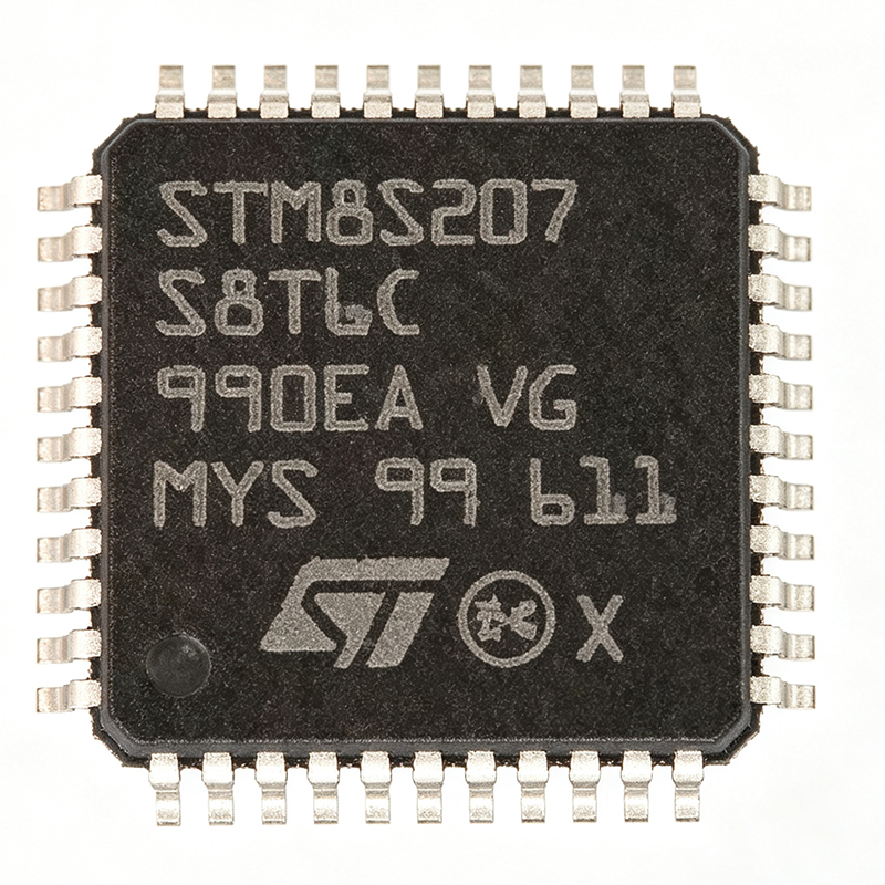
Quick Answers: What is the STM8S207S8T6 and Is It Available?
The STM8S207S8T6 is a performance-line 8-bit microcontroller from STMicroelectronics, operating at up to 24 MHz with 64 KB of Flash program memory. It integrates a 10-bit ADC, multiple timers, two UARTs, SPI, I2C, and CAN 2.0B, and is housed in a 44-pin LQFP package. As of 2026-08-28, the STM8S207S8T6 is in stock at XAIPART with 99,999 units available, priced at $2.3864 per unit for quantities of 1000 or more (MOQ 1). The device operates from 3.3V to 5V, with a temperature range of -40°C to +85°C, making it suitable for industrial, automotive, and consumer applications.
Technical Guide: How to Select, Design In, and Use the STM8S207S8T6
Understanding the Core and Memory
The STM8S207S8T6 is built on the STM8 8-bit CISC core, achieving up to 20 MIPS at 24 MHz. It provides 64 KB of Flash program memory, 2 KB of data EEPROM, and 6 KB of RAM. This memory configuration supports complex control algorithms and data logging without external memory. The 2 KB EEPROM is ideal for storing calibration parameters and user settings, reducing BOM cost.
Peripheral Set and Connectivity
The MCU includes a 10-bit ADC with 16 multiplexed channels, enabling precise analog sensor readings. It offers two UARTs, one SPI, one I2C, and a CAN 2.0B interface, providing flexible communication options for industrial networks and automotive systems. The timer suite includes one 16-bit advanced control timer, two 16-bit general-purpose timers, and one 8-bit basic timer, suitable for PWM generation, motor control, and time-base generation.
Power Supply and Decoupling
The STM8S207S8T6 operates from a 3.3V or 5V supply. For reliable operation, place 100 nF decoupling capacitors close to the VDD and VDDA pins (pins 8 and 42). The VDDA pin powers the ADC, and VSSA (pin 43) is the analog ground. Ensure a clean analog supply to minimize ADC noise.
Clock Configuration
The device supports multiple clock sources: internal RC, external crystal, or PLL. For cost-sensitive designs, the internal RC oscillator is sufficient. For precise timing (e.g., CAN communication), use an external crystal. The CLK_CCO pin (pin 36) can output the clock for synchronization.
Programming and Debugging
The STM8S207S8T6 supports in-circuit programming and debugging via the SWIM interface (pin 35). A single-wire connection to an ST-LINK programmer enables firmware updates and debugging. This simplifies development and field updates.
Design Considerations
When designing with this MCU, consider the following:
- I/O Tolerance: The device is 5V tolerant, allowing direct connection to legacy sensors and actuators without level shifters.
- Watchdog Timer: Use the built-in watchdog to enhance system reliability in noisy environments.
- Low-Power Modes: The MCU offers multiple low-power modes to extend battery life in portable applications.
- Thermal Management: The LQFP-44 package (10x10 mm, 0.8 mm pitch) dissipates heat adequately for typical applications; ensure proper PCB layout for high-current I/O.
Alternatives & Comparison: Drop-In Replacements and Other Options
For engineers seeking alternatives, the STM8S207S8T6B is a pin-compatible drop-in replacement with automotive-grade qualification. The STM8S207S8T6C offers an extended temperature range, and the STM8S207S8T6TR is the tape-and-reel packaging variant. The STM8S207R8T6 is not pin-compatible due to its 64-pin package. The table below compares the STM8S207S8T6 with its direct alternatives based on verified data.
| Parameter | STM8S207S8T6 | STM8S207S8T6B | STM8S207S8T6C | STM8S207S8T6TR |
|---|---|---|---|---|
| Package | LQFP-44 | LQFP-44 | LQFP-44 | LQFP-44 |
| Pin Compatibility | Reference | Yes | Yes | Yes |
| Automotive Grade | No | Yes | No | No |
| Extended Temperature | -40°C to +85°C | [DATA_NEEDED: temperature range] | Yes | [DATA_NEEDED: temperature range] |
| Packaging | Tray | Tray | Tray | Tape & Reel |
For a lower-cost option with reduced features, consider the STM8S105C6T6, but note it has 32 KB Flash, 16 MHz clock, and no CAN interface, so it is not a drop-in replacement.
Industry Insight: Market Position, Lifecycle, and Supply
The STM8S207S8T6 is currently in an active lifecycle status, indicating ongoing production and availability. As of 2026-08-28, XAIPART holds 99,999 units in stock, ensuring immediate availability for orders of any quantity (MOQ 1). The pricing tiers are as follows: $4.0909 (1+), $2.9545 (10+), $2.6136 (100+), $2.5 (500+), and $2.3864 (1000+). This volume-based pricing supports both prototyping and mass production. The STM8 family remains a popular choice for cost-sensitive 8-bit applications, and the STM8S207S8T6's CAN interface positions it well for automotive and industrial networking. [DATA_NEEDED: market share data]
Trends & Outlook: What Buyers Should Watch
The 8-bit MCU market continues to thrive in applications where cost and simplicity outweigh raw processing power. The STM8S207S8T6's 24 MHz clock, 64 KB Flash, and CAN 2.0B interface make it a strong contender for next-generation industrial and automotive designs. Buyers should monitor the availability of the automotive-grade STM8S207S8T6B for AEC-Q100 requirements. Additionally, the trend toward smart home and IoT devices favors MCUs with low power consumption and rich connectivity, both of which the STM8S207S8T6 offers. As supply chains stabilize, expect stable pricing and lead times. [VERIFY_NEEDED: future product roadmap]
Comments
Be the first to comment.
🔐 Please sign in to post a comment.
Don't have an account? Sign up