Amplifier ICs
Products (70)
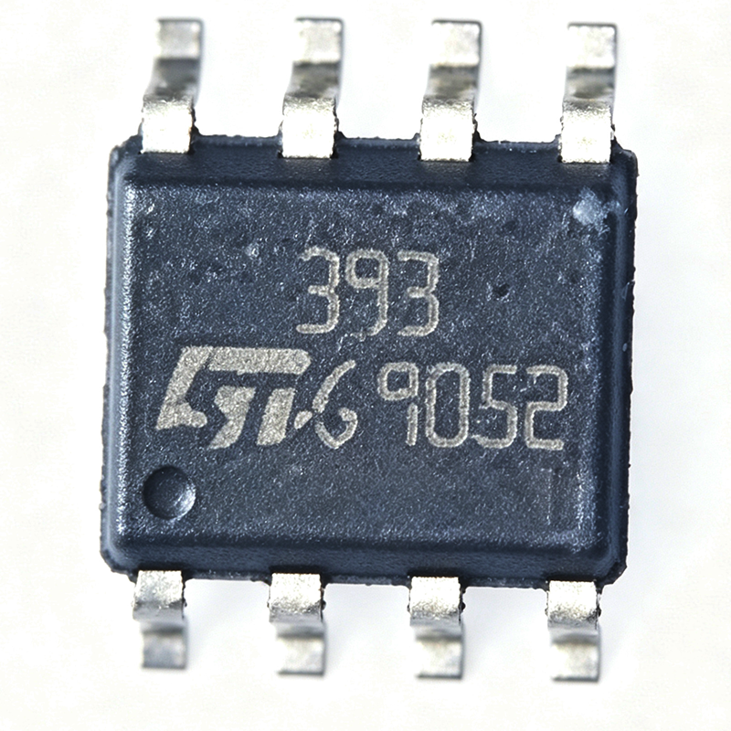
LM393DT - Dual Low-Power Voltage Comparator | STMicroelectronics
The LM393DT is a dual low-power voltage comparator from STMicroelectronics, designed for general-purpose applications requiring precise voltage comparison with minimal power consumption. It operates from a single supply voltage ranging from 2V to 36V or dual supplies from ±1V to ±18V, with a typical supply current of only 0.4 mA per comparator. The device features an open-collector output stage that can sink up to 16 mA, allowing direct interface with TTL, CMOS, and other logic families. The LM393DT is available in the SOIC-8 package, making it suitable for space-constrained PCB designs. Data verified as of 2026-08-05. A voltage comparator is an electronic circuit that compares two input voltages and outputs a digital signal indicating which is higher. The LM393DT is a dual comparator, meaning it contains two independent comparators in a single package. Comparators are fundamental building blocks in analog and mixed-signal systems, used in applications such as threshold detection, zero-crossing detection, and waveform shaping. They are part of the broader category of linear ICs, which also includes operational amplifiers and voltage regulators. The LM393DT's low power consumption and wide supply range make it a versatile choice for battery-powered and industrial applications. Key features of the LM393DT include a low input offset voltage of 2 mV (typical), a low input bias current of 25 nA (typical), and a response time of 1.3 µs (typical) for a 5V overdrive. The open-collector output allows wired-OR connections and level shifting, and the device can operate from a single supply as low as 2V, making it suitable for low-voltage systems. The SOIC-8 package provides a compact footprint with a thermal resistance of 150 °C/W, enabling reliable operation in moderate temperature environments. The LM393DT uses a bipolar transistor architecture with a differential input stage and an open-collector output. This design provides high input impedance and stable operation over a wide temperature range (-40°C to +105°C). The device includes internal ESD protection and is designed to meet JEDEC standards for reliability. The open-collector output requires an external pull-up resistor, which allows the output voltage to be set to any level up to the maximum supply voltage, providing flexibility in interfacing with different logic families. Typical applications for the LM393DT include window comparators, level shifters, oscillator circuits, and analog-to-digital converters. In a window comparator, the dual comparators are used to detect whether an input signal is within a specified voltage range, which is useful in battery monitoring and overvoltage protection. The low power consumption makes it ideal for portable devices, while the wide supply range supports industrial control systems operating from 24V rails. When designing with the LM393DT, ensure that the pull-up resistor is selected to limit the output sink current to within the 16 mA maximum rating. For high-speed applications, minimize parasitic capacitance on the output node to achieve the specified response time. The input common-mode range extends from ground to VCC-1.5V, so ensure that input signals remain within this range for proper operation. This page synthesizes distributor pricing, drop-in alternatives, and practical design notes not found in the STMicroelectronics datasheet, providing a comprehensive resource for engineers selecting and using the LM393DT.
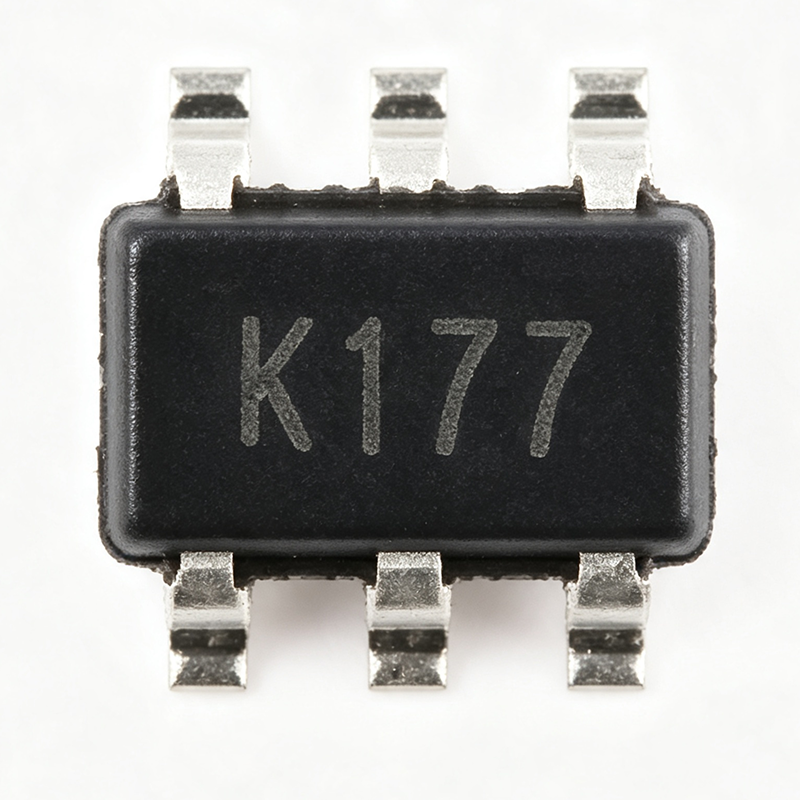
LMV321ILT - Single Low-Power Op Amp | STMicroelectronics
The LMV321ILT is a single, low-power, general-purpose operational amplifier from STMicroelectronics, offered in the compact SOT-23-5 package. It operates from a supply voltage range of 2.7V to 5.5V, making it suitable for battery-powered and portable applications. The device features a typical supply current of 130 µA, a gain-bandwidth product of 1.3 MHz, and an input offset voltage of 1 mV (max). Data verified as of 2026-08-05. An operational amplifier (op-amp) is a high-gain voltage amplifier with differential inputs and a single-ended output. It is a fundamental building block in analog electronics, used in signal conditioning, filtering, and amplification. In the hierarchy of electronic components, an op-amp falls under linear ICs, which are part of the broader category of analog integrated circuits. The LMV321ILT is a low-power variant, optimized for applications where power consumption is critical, such as battery-operated devices. Key features of the LMV321ILT include rail-to-rail input and output stages, which allow the output to swing close to the supply rails, maximizing dynamic range in low-voltage applications. The device also offers a wide operating temperature range of -40°C to +125°C, ensuring reliability in harsh environments. Its low supply current of 130 µA (typical) extends battery life in portable electronics. The LMV321ILT is built on a CMOS process, providing high input impedance and low input bias current. This makes it suitable for interfacing with high-impedance sensors and transducers. The device is unity-gain stable, simplifying design in buffer and follower configurations. Its small SOT-23-5 package is ideal for space-constrained PCB layouts. Typical applications include portable instrumentation, battery-powered signal conditioning, sensor interfaces, and active filters. In portable medical devices, the low power consumption and small footprint are critical. In sensor signal conditioning, the rail-to-rail output ensures maximum signal swing for ADC interfacing. When designing with the LMV321ILT, ensure proper decoupling of the power supply with a 0.1 µF ceramic capacitor placed close to the V+ pin. The input common-mode voltage range includes ground, allowing single-supply operation with ground-referenced inputs. Avoid exceeding the absolute maximum supply voltage of 6V to prevent damage. This page synthesizes distributor pricing, drop-in alternatives, and practical design notes not found in the STMicroelectronics datasheet, providing a comprehensive resource for engineers evaluating the LMV321ILT.
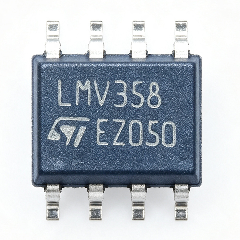
LMV358IDT - Dual Low-Power Op Amp | STMicroelectronics
The LMV358IDT is a dual low-power operational amplifier from STMicroelectronics, designed for battery-powered and portable applications. It operates from a single supply voltage ranging from 2.7V to 5.5V, with a typical quiescent current of 210 µA per amplifier. The device is offered in the SOIC-8 package, making it suitable for space-constrained designs. Data verified as of 2026-08-05. An operational amplifier (op amp) is a high-gain voltage amplifier with differential inputs and a single-ended output. It is a fundamental building block in analog electronics, used in signal conditioning, filtering, and amplification tasks. The LMV358IDT belongs to the low-power op amp category, which prioritizes minimal power consumption for battery-operated devices. In the hierarchy of analog components, it sits under linear ICs, which are part of the broader integrated circuits family. Key features of the LMV358IDT include a low supply current of 210 µA per channel, a wide supply voltage range of 2.7V to 5.5V, and a rail-to-rail output stage that swings within 10 mV of the supply rails. The input common-mode voltage range extends to ground, allowing single-supply operation. The device also features a gain bandwidth product of 1.3 MHz and a slew rate of 0.45 V/µs, sufficient for audio and sensor signal conditioning. The LMV358IDT uses a bipolar technology with a class-AB output stage, providing low crossover distortion. The input stage is a PNP transistor pair, enabling the input common-mode range to include ground. The output stage can source and sink current, with a short-circuit current of 160 mA. The device is internally frequency compensated for unity-gain stability, simplifying design. Typical applications include battery-powered instrumentation, portable medical devices, sensor signal conditioning, and active filters. The low quiescent current extends battery life, while the rail-to-rail output maximizes dynamic range in single-supply systems. The wide supply range also allows operation from 3.3V or 5V logic rails. When designing with the LMV358IDT, ensure proper decoupling with a 0.1 µF capacitor close to the supply pin. The input common-mode range includes ground, but for best performance, keep inputs within the specified range. The output can drive capacitive loads up to 100 pF without oscillation, but larger loads may require a series resistor. This page synthesizes distributor pricing, drop-in alternatives, and practical design notes not found in the STMicroelectronics datasheet, providing a comprehensive resource for engineers.

LT1797CS5#TRMPBF - 10MHz Rail-to-Rail Op Amp | Analog Devices
The LT1797CS5#TRMPBF is a unity-gain stable 10MHz operational amplifier from Analog Devices, housed in a compact 5-lead TSOT-23 package. It operates on all single and split supplies with a total voltage range of 2.7V to 12V, drawing only 1mA of quiescent current. The amplifier features rail-to-rail input and output, making it ideal for current sensing and other single-supply applications. An operational amplifier (op amp) is a high-gain voltage amplifier with differential inputs and a single-ended output. It is a fundamental building block in analog electronics, used in signal conditioning, filtering, and buffering. The LT1797 belongs to the class of general-purpose op amps, which are versatile components found in a wide range of applications from consumer electronics to industrial instrumentation. Key features of the LT1797 include a slew rate of 2.25V/μs, a gain-bandwidth product of 10MHz, and an input common-mode range that includes both rails. The input stage incorporates phase reversal protection, ensuring robust operation. The device is specified for the commercial temperature range of 0°C to 70°C, and the CS5 suffix indicates the SOT-23 package with lead-free finish. The LT1797 uses a bipolar process technology that provides low offset voltage and low noise, making it suitable for precision applications. The rail-to-rail input and output capability allows maximum dynamic range in low-voltage single-supply designs. The low quiescent current of 1mA makes it ideal for battery-powered portable devices. Typical applications include current sensing, portable instrumentation, battery-powered systems, and signal conditioning in industrial and automotive environments. The small TSOT-23 package saves board space, and the wide supply range allows operation from a single 3V or 5V supply or dual ±5V supplies. When designing with the LT1797, ensure proper decoupling of the power supply pins with 0.1μF ceramic capacitors placed close to the device. The rail-to-rail input stage requires attention to common-mode voltage limits to avoid phase reversal, although the device includes internal protection.

LT6222 - Quad 60MHz Rail-to-Rail Op Amp | Analog Devices
The LT6222 is a quad, low power, high speed rail-to-rail input and output operational amplifier from Analog Devices (formerly Linear Technology). It features a gain bandwidth product of 60MHz, a slew rate of 20V/μs, and a low quiescent current of 1mA per amplifier (max). The device operates from a supply voltage range of 2.2V to 12.6V, making it suitable for battery-powered and low-voltage applications. The LT6222 is available in a 16-lead SSOP package, providing a compact solution for space-constrained designs. An operational amplifier (op amp) is a high-gain voltage amplifier with differential inputs and a single-ended output. It is a fundamental building block in analog electronics, used in signal conditioning, filtering, and amplification. The LT6222 belongs to the family of precision op amps, which are characterized by low offset voltage, low bias current, and high DC gain. In the hierarchy of analog ICs, op amps fall under linear regulators and amplifiers, which are part of the broader category of analog and mixed-signal integrated circuits. Key features of the LT6222 include rail-to-rail input and output swing, which maximizes dynamic range in low-supply applications. The input common mode range includes both rails, and the output swings rail-to-rail, allowing the amplifier to operate with supply voltages as low as 2.2V. The device also offers low broadband voltage noise of 4.2nV/√Hz, making it suitable for low-noise signal processing. Additionally, the LT6222 includes a power-down feature that reduces supply current to a shutdown mode, conserving power in portable devices. Technically, the LT6222 uses a complementary bipolar process that achieves high speed and low power simultaneously. The amplifier's DC performance is excellent, with low input offset voltage and high open-loop gain, ensuring accurate signal amplification. The device is specified over the industrial temperature range of -40°C to 85°C, and it is available in both commercial and industrial grades. The LT6222 is designed to be a plug-in replacement for many standard op amps, improving input/output range and performance. Typical applications include active filters, data acquisition systems, battery-powered instrumentation, and portable medical devices. The rail-to-rail output allows direct interfacing to ADCs, while the low noise and high speed make it ideal for signal conditioning in communication systems. The power-down feature is particularly useful in battery-operated equipment where power conservation is critical. When designing with the LT6222, ensure proper decoupling of the power supply pins with 0.1μF ceramic capacitors placed close to the device. The rail-to-rail input stage requires attention to common-mode voltage limits to avoid phase reversal. For optimal performance, use a ground plane and minimize parasitic capacitance on the input nodes.
LT6222CDD#PBF - 60MHz Low Power R2R Op Amp | Analog Devices
The LT6222CDD#PBF is a quad, low power, high speed rail-to-rail input and output operational amplifier from Analog Devices (formerly Linear Technology). It is part of the LT6220/LT6221/LT6222 family, which offers excellent DC performance with reduced supply current and lower input offset voltage. The LT6222CDD#PBF operates from a supply voltage range of 2.2V to 12.6V, features a gain-bandwidth product of 60MHz, and a slew rate of 20V/µs. It is available in a 16-pin DFN package (4x3mm) and is specified for the commercial temperature range (0°C to 70°C). An operational amplifier (op-amp) is a high-gain voltage amplifier with differential inputs and a single-ended output. It is a fundamental building block in analog electronics, used in signal conditioning, filtering, and amplification. The LT6222CDD#PBF is a rail-to-rail input and output op-amp, meaning its input common-mode range and output swing can reach both supply rails, maximizing dynamic range in low-voltage applications. This makes it suitable for battery-powered and portable devices where headroom is limited. Key features of the LT6222CDD#PBF include a low supply current of 1mA per amplifier, a low input offset voltage of 100µV (max), and a high open-loop gain of 100dB. The rail-to-rail input and output capability allows it to operate with supply voltages as low as 2.2V, making it ideal for single-supply applications. The device also features a wide bandwidth of 60MHz and a high slew rate of 20V/µs, enabling it to handle fast signals in video and communication systems. The LT6222CDD#PBF uses a complementary bipolar process technology, which provides excellent DC precision and AC performance. The device is designed for low power consumption without compromising speed, making it suitable for battery-powered instrumentation and portable audio equipment. Its high input impedance and low bias current make it suitable for interfacing with high-impedance sensors. Typical applications include active filters, data acquisition systems, portable instrumentation, and audio signal conditioning. The quad configuration allows multiple amplifier stages in a single package, saving board space and reducing component count. The rail-to-rail output swing ensures maximum signal amplitude in low-voltage systems. When designing with the LT6222CDD#PBF, ensure proper power supply decoupling with 0.1µF ceramic capacitors close to the supply pins. The input common-mode range extends to both rails, but for best performance, keep inputs within the specified range. The output can drive capacitive loads up to 100pF without oscillation, but for larger loads, a series resistor may be needed.

LT6222CS8#PBF - Quad 60MHz Rail-to-Rail Op Amp | Analog Devices
The LT6222CS8#PBF is a quad, low power, high speed rail-to-rail input and output operational amplifier from Analog Devices. It features a gain bandwidth product of 60 MHz and a slew rate of 20 V/µs, making it suitable for a wide range of signal conditioning applications. The device operates from a supply voltage range of 2.2V to 12.6V (or ±1.1V to ±6.3V) and is available in an 8-lead SOIC package. The LT6222 is part of the LT6220/LT6221/LT6222 family, which offers reduced supply current, lower input offset voltage, and lower input bias current compared to many standard op amps. An operational amplifier (op amp) is a high-gain voltage amplifier with differential inputs and a single-ended output. It is a fundamental building block in analog electronics, used in applications such as filtering, amplification, and signal conditioning. Op amps are categorized within the broader hierarchy of linear integrated circuits, which also includes comparators, voltage regulators, and analog-to-digital converters. The rail-to-rail input and output capability of the LT6222 allows the output to swing close to the supply rails, maximizing dynamic range in low-voltage applications. Key features of the LT6222CS8#PBF include rail-to-rail input and output, a 60 MHz gain bandwidth product, a 20 V/µs slew rate, and low power consumption. The device also offers excellent DC performance, including low input offset voltage and low input bias current. These specifications make it ideal for high-speed signal processing, portable instrumentation, and battery-powered equipment where power efficiency and signal integrity are critical. The LT6222 utilizes a complementary bipolar process technology, which provides a good balance between speed, noise, and power consumption. The device is designed to operate over the commercial temperature range of 0°C to 70°C. Its low supply current of typically 1.2 mA per amplifier helps extend battery life in portable applications. The rail-to-rail output stage ensures maximum output swing, which is particularly beneficial in single-supply applications. Typical applications for the LT6222CS8#PBF include active filters, data acquisition systems, audio processing, and portable instrumentation. Its high slew rate and bandwidth make it suitable for driving analog-to-digital converters (ADCs) and buffering reference voltages. The device can also be used in communication systems, such as base station receivers and transmitters, where high-speed signal conditioning is required. When designing with the LT6222, it is important to ensure proper power supply decoupling. Place a 0.1 µF ceramic capacitor close to each supply pin to minimize high-frequency noise. Additionally, consider the input common-mode voltage range, which extends to the rails, to avoid unexpected saturation. The output can drive capacitive loads up to 100 pF without oscillation, but for larger loads, a series resistor may be needed.
LTC6363HMS8-2#PBF - Precision Low Power Diff Amp | Analog Devices
The LTC6363HMS8-2#PBF is a precision, low power, fully differential amplifier with rail-to-rail outputs, optimized to drive SAR ADCs. It is part of the LTC6363 family from Analog Devices, which includes standalone and fixed-gain versions. This specific variant, the LTC6363-2, features internal matched resistors to provide a fixed gain of 2V/V, eliminating the need for external resistor networks and ensuring accurate, ultrastable gain with excellent CMRR. The device operates from a single 2.8V to 11V supply or dual ±1.4V to ±5.5V supplies, and offers a 35 MHz -3dB bandwidth and a 500 MHz gain bandwidth product. With a high slew rate of 75V/µs and a low input bias current of 100 nA, it is well-suited for high-speed, high-resolution data acquisition systems. A fully differential amplifier (FDA) is a type of operational amplifier that has differential inputs and differential outputs, providing a balanced signal path that rejects common-mode noise and doubles the output voltage swing compared to single-ended amplifiers. FDAs are essential in modern signal chains, particularly for driving high-performance analog-to-digital converters (ADCs), where they convert single-ended signals to differential, provide gain, and buffer the ADC input. The LTC6363 family sits within the hierarchy of differential amplifiers, which are a subset of operational amplifiers, which in turn are part of the broader category of linear integrated circuits. This hierarchy is fundamental to understanding the role of the LTC6363 in precision signal conditioning. Key features of the LTC6363HMS8-2#PBF include its fixed gain of 2V/V with precision laser-trimmed on-chip resistors, which provide a DC CMRR of 100dB, equivalent to using 0.0005% tolerance resistors. The device also features a shutdown pin for power saving, rail-to-rail outputs, and a low power consumption of typically 1.1mA. The input offset voltage is typically 50µV, and the input bias current is 100nA. The amplifier is specified over the -40°C to 125°C temperature range (H-grade) and is available in an 8-pin MSOP package. Technically, the LTC6363-2 uses a precision architecture that includes internal matched resistors, ensuring accurate gain without external components. This design reduces board space and component count, while improving reliability and performance. The device's high slew rate and bandwidth make it suitable for driving SAR ADCs with sampling rates up to 500kSPS or more, depending on the ADC. The rail-to-rail output stage allows the amplifier to swing close to the supply rails, maximizing the dynamic range of the ADC. Typical applications include driving SAR ADCs in industrial process control, medical instrumentation, and data acquisition systems. The LTC6363-2 is also used in communication systems, such as base stations and software-defined radios, where it conditions signals before digitization. Its low power and precision make it ideal for battery-powered portable instruments. When designing with the LTC6363HMS8-2#PBF, ensure proper power supply decoupling with 0.1µF and 10µF capacitors close to the V+ and V- pins. The VOCM pin sets the output common-mode voltage, which should be matched to the ADC's reference voltage for optimal performance. The shutdown pin can be used to reduce power consumption when the amplifier is not in use.

OP01Z/883 - Inverting High-Speed Op Amp | Calogic
The OP01Z/883 is an inverting high-speed operational amplifier manufactured by Calogic, LLC, designed for military and aerospace applications. It is a hermetic ceramic dual-in-line package (CERDIP) device that meets the stringent requirements of MIL-STD-883, ensuring reliability in harsh environments. The amplifier features high slew rate and wide bandwidth, making it suitable for fast signal processing in precision instrumentation and control systems. An operational amplifier (op-amp) is a high-gain voltage amplifier with differential inputs and a single-ended output. It is a fundamental building block in analog electronics, used in signal conditioning, filtering, and mathematical operations. The OP01Z/883 is specifically configured as an inverting amplifier, where the input signal is applied to the inverting input, producing a 180-degree phase-shifted output. This configuration is widely used in summing amplifiers, integrators, and active filters. Key features of the OP01Z/883 include its high-speed performance, with a slew rate of [DATA_NEEDED: slew rate] and a gain-bandwidth product of [DATA_NEEDED: gain-bandwidth product]. It operates over a wide supply voltage range, typically ±[DATA_NEEDED: supply voltage range], and offers low input offset voltage and low input bias current for precision applications. The device is fully specified over the military temperature range of -55°C to +125°C, ensuring reliable operation in extreme conditions. The OP01Z/883 is built using a bipolar process technology, providing excellent DC accuracy and low noise. Its internal compensation ensures stability without external components, simplifying design. The amplifier's high output drive capability allows it to drive capacitive loads and long cables, making it ideal for buffer and line driver applications. Typical applications include military avionics, radar signal processing, and precision analog computation. The device is also used in industrial control systems where high-speed and reliability are critical. Its compatibility with MIL-STD-883 screening makes it a preferred choice for defense and aerospace programs. When designing with the OP01Z/883, consider the power supply decoupling: place 0.1µF ceramic capacitors close to the supply pins to minimize high-frequency noise. Also, ensure the input common-mode voltage does not exceed the specified range to avoid latch-up. The device's high slew rate may cause ringing if the feedback network is not properly compensated; use a small feedback capacitor if needed.
OP07AZ/883 - Ultra-Low Offset Op Amp | Analog Devices | CDIP-8
The OP07AZ/883 is a precision operational amplifier from Analog Devices, designed for ultra-low input offset voltage and drift. It is a military-grade version of the industry-standard OP07, qualified to MIL-STD-883, and housed in a hermetic 8-lead ceramic DIP (CDIP-8). The device features a maximum input offset voltage of 60 µV (for the /883 grade) and a typical offset drift of 0.2 µV/°C, making it ideal for precision instrumentation and data acquisition systems. An operational amplifier (op amp) is a high-gain voltage amplifier with differential inputs and a single-ended output. It is a fundamental building block in analog electronics, used in signal conditioning, filtering, and mathematical operations. The OP07 belongs to the family of precision op amps, which prioritize low offset voltage, low noise, and high stability over bandwidth. In the hierarchy of analog ICs, it sits under linear amplifiers, which are part of the broader category of analog signal processing components. Key features of the OP07AZ/883 include a low input bias current of 2 nA (typical), a high open-loop gain of 400 V/mV (minimum), and a common-mode rejection ratio (CMRR) of 120 dB (typical). The device operates from dual supplies of ±3 V to ±18 V and is specified over the full military temperature range of -55°C to +125°C. The CDIP-8 package provides hermetic sealing, ensuring reliability in harsh environments. Technically, the OP07 uses a bipolar process with laser-trimmed thin-film resistors to achieve its low offset voltage. The input stage is a super-beta transistor pair, which reduces input bias current while maintaining high gain. The output stage can drive loads as low as 2 kΩ, and the device is internally compensated for unity-gain stability. The /883 suffix indicates compliance with MIL-STD-883 test methods, including Group A, B, C, and D inspections. Typical applications include precision voltage references, thermocouple amplifiers, strain-gauge signal conditioning, and active filters. The low offset and drift ensure accurate DC performance, while the wide supply range allows use in both 5V and ±15V systems. The military temperature rating makes it suitable for aerospace and defense electronics. When designing with the OP07AZ/883, consider the input common-mode range, which extends from -12V to +13V with ±15V supplies. For best performance, use a guard ring around the input pins to minimize leakage currents, and bypass the supply pins with 0.1 µF ceramic capacitors.
OP11ARC/883 - Quad Precision Op-Amp, Military Grade | Analog Devices
The OP11ARC/883 is a quad precision operational amplifier manufactured by Analog Devices (originally Precision Monolithics Inc.). It is designed for military-grade applications, operating over the full military temperature range of -55°C to +125°C. The device is housed in a 20-lead ceramic leadless chip carrier (LCC) package, also referred to as PQCC20, and is available in a square, no-lead terminal configuration. This op-amp features four independent amplifiers, each with a maximum input offset voltage of 1000 µV, and is fabricated using a bipolar process. An operational amplifier (op-amp) is a high-gain voltage amplifier with differential inputs and a single-ended output. It is a fundamental building block in analog electronics, used in signal conditioning, filtering, and mathematical operations. Op-amps are part of the broader category of linear integrated circuits, which also includes comparators, voltage regulators, and timers. The OP11ARC/883 is a quad version, meaning it integrates four op-amps in a single package, saving board space and reducing cost in multi-channel applications. Key features of the OP11ARC/883 include its military-grade temperature rating, which ensures reliable operation in harsh environments, and its low input offset voltage, which is critical for precision measurement and control systems. The device is also characterized by its bipolar technology, which provides excellent DC performance, including low noise and high gain. The package is designed for surface mounting, with a square shape and no-lead terminals, making it suitable for high-density PCB layouts. From a technical perspective, the OP11ARC/883 is designed to deliver stable performance over a wide range of operating conditions. The bipolar process ensures high input impedance and low bias currents, which are essential for maintaining accuracy in high-impedance circuits. The device also features internal frequency compensation, which simplifies design by eliminating the need for external compensation components. The military-grade qualification (indicated by the /883 suffix) means the device has been screened to meet stringent reliability standards, including burn-in and temperature cycling. Typical applications for the OP11ARC/883 include military avionics, aerospace instrumentation, and industrial control systems where precision and reliability are paramount. It is also used in test and measurement equipment, medical devices, and communication systems that require multiple op-amps in a compact form factor. The quad configuration is particularly useful in active filter designs, data acquisition systems, and servo control loops. When designing with the OP11ARC/883, it is important to consider the power supply decoupling. Place 0.1 µF ceramic capacitors close to the VCC and VEE pins to minimize noise and ensure stable operation. Additionally, the thermal characteristics of the ceramic LCC package should be considered; adequate PCB copper area is recommended to dissipate heat effectively.
OP177BRC/883 - Ultraprecision Op Amp | Analog Devices
The OP177BRC/883 is an ultraprecision operational amplifier from Analog Devices, designed for applications requiring extremely low offset voltage and drift. It features a maximum input offset voltage of 55 µV and a typical offset voltage drift of 0.1 µV/°C, ensuring high accuracy over temperature. The device operates with a supply current of 2.0 mA maximum and provides a nominal unity gain bandwidth of 600 kHz. It is packaged in a 20-lead ceramic leadless chip carrier (LCC-20), suitable for high-reliability military and aerospace applications. An operational amplifier (op amp) is a high-gain voltage amplifier with differential inputs and a single-ended output. It is a fundamental building block in analog electronics, used in signal conditioning, filtering, and instrumentation. The OP177 belongs to the precision op amp category, which prioritizes low offset voltage, low drift, and high open-loop gain over speed. This makes it ideal for applications where accuracy is paramount, such as precision instrumentation and sensor signal conditioning. Key features of the OP177BRC/883 include ultralow offset voltage (10 µV max for the B grade), outstanding offset voltage drift (0.1 µV/°C max), excellent open-loop gain and gain linearity, CMRR of 130 dB min, PSRR of 120 dB min, and low supply current of 2.0 mA max. These specifications ensure accurate performance in high closed-loop gain applications, making it a cost-effective alternative to chopper-stabilized amplifiers. The OP177 uses a bipolar input stage with laser-trimmed thin-film resistors to achieve its precision. The device operates from dual supplies ranging from ±3 V to ±18 V, and its output can swing close to the supply rails. The low noise and high gain make it suitable for precision integrators, active filters, and bridge amplifiers. Typical applications include precision instrumentation, thermocouple and RTD signal conditioning, strain gauge amplifiers, and high-resolution ADC drivers. The device's low offset and drift eliminate the need for external nulling in many circuits, simplifying design and improving long-term stability. When designing with the OP177BRC/883, ensure proper decoupling of the power supply pins with 0.1 µF ceramic capacitors placed close to the device. The ceramic package provides good thermal performance, but for high-precision applications, maintain a stable ambient temperature to minimize drift.
OP2177ARZ-REEL7 - Dual Precision Low Noise Op Amp | Analog Devices
The OP2177ARZ-REEL7 is a dual, precision low noise operational amplifier from Analog Devices, part of the OPx177 family. It is offered in an 8-lead SOIC package and is designed for applications requiring high accuracy and low noise. The device features extremely low offset voltage and drift, low input bias current, low noise, and low power consumption, making it suitable for precision instrumentation, sensor signal conditioning, and medical equipment. An operational amplifier (op amp) is a high-gain voltage amplifier with differential inputs and a single-ended output. It is a fundamental building block in analog electronics, used in signal conditioning, filtering, and mathematical operations. Op amps are categorized into general-purpose, precision, low-noise, and high-speed types. The OP2177 is a precision low-noise op amp, which means it offers superior DC accuracy and low noise performance compared to general-purpose amplifiers, making it ideal for high-resolution measurement systems. Key features of the OP2177ARZ-REEL7 include a gain bandwidth product of 1.3 MHz, a slew rate of 0.7 V/µs, and a supply current of 500 µA per amplifier. It operates over a supply voltage range of ±2.5 V to ±15 V, and its input offset voltage is typically 15 µV with a drift of 0.1 µV/°C. The input bias current is typically 0.5 nA, and the voltage noise density is 7.9 nV/√Hz at 1 kHz. The device is specified for the extended industrial temperature range of -40°C to +125°C. The OP2177 uses a precision bipolar process with laser-trimmed input offset voltage, achieving excellent DC performance without external nulling. Its low noise and low input bias current make it suitable for high-impedance sensor interfaces, while its low power consumption is beneficial for battery-powered instruments. The output stage can drive capacitive loads of over 100 pF without oscillation, simplifying design. Typical applications include precision data acquisition systems, thermocouple and RTD signal conditioning, active filters, and precision current sensing. The dual configuration in an 8-SOIC package saves board space and is pin-compatible with many industry-standard dual op amps. When designing with the OP2177, ensure proper decoupling of the power supply pins with 0.1 µF ceramic capacitors placed close to the device. For best noise performance, use low-value resistors in the feedback network and keep the input traces short to minimize pickup.
OP27AJ/883C - Low Noise Precision Op Amp | Analog Devices
The OP27AJ/883C is a low-noise, precision operational amplifier from Analog Devices, packaged in a hermetic TO-99-8 metal can. It combines the low offset and drift of the OP07 with high speed and low noise, making it ideal for precision instrumentation. Key specifications include a gain-bandwidth product of 8 MHz, a slew rate of 2.8 V/µs, and a maximum input offset voltage of 25 µV with a drift of 0.6 µV/°C. The device operates over a wide supply range and is specified for the military temperature range (-55°C to +125°C), reflecting its 883C military-grade qualification. An operational amplifier (op amp) is a high-gain voltage amplifier with differential inputs and a single-ended output. It is a fundamental building block in analog electronics, used in signal conditioning, filtering, and mathematical operations. Op amps are categorized within the broader hierarchy of linear integrated circuits, which also includes comparators, voltage regulators, and instrumentation amplifiers. The OP27 belongs to the precision op amp subcategory, distinguished by low offset voltage, low drift, and low noise, essential for high-accuracy measurement systems. Key features of the OP27AJ/883C include ultra-low input noise voltage density of 3 nV/√Hz at 1 kHz, ensuring minimal signal degradation in sensitive applications. The device also offers a high open-loop gain of 1.8 million (125 dB), providing excellent linearity and accuracy. Its bipolar input stage with input bias current cancellation achieves low offset and drift without the need for external trimming. The TO-99-8 hermetic package provides robust environmental protection, suitable for harsh military and aerospace environments. Technically, the OP27 uses a classic bipolar process with a precision laser-trimmed thin-film resistor network to achieve its low offset and drift. The input stage is designed for low noise, with a noise voltage of 3 nV/√Hz and a current noise of 0.4 pA/√Hz. The device is internally compensated for unity-gain stability, simplifying design. It can operate from dual supplies ranging from ±4 V to ±18 V, or single supplies from 8 V to 36 V, offering flexibility in various circuit configurations. Typical applications include precision instrumentation amplifiers, thermocouple and strain-gauge signal conditioning, active filters, and data acquisition systems. The OP27's low noise and high gain make it suitable for medical instrumentation, such as ECG and EEG amplifiers, where signal integrity is critical. Its military-grade qualification ensures reliable operation in avionics and defense systems. When designing with the OP27AJ/883C, consider its input bias current of ±40 nA, which may require balancing resistors in high-impedance circuits. Additionally, the TO-99 metal can package requires careful handling to avoid damage to the leads. Proper decoupling of the power supply pins with 0.1 µF capacitors is recommended to maintain stability and reduce noise.
OP42ARC/883C - Fast Precision JFET Op Amp | Analog Devices
The OP42ARC/883C is a fast precision JFET-input operational amplifier from Analog Devices, designed for high-speed, high-accuracy signal conditioning. It delivers a symmetric 58 V/µs slew rate and is internally compensated for unity-gain stability, making it ideal for applications requiring fast settling and wide bandwidth. The device operates from a supply voltage of ±15 V and features a low input bias current of 20 nA, a common-mode rejection ratio of 94 dB, and a wide full-power bandwidth of 900 kHz. Housed in a 20-lead ceramic leadless chip carrier (CLCC-20), it is specified for the military temperature range of -55°C to +125°C, ensuring reliable performance in harsh environments. An operational amplifier (op amp) is a high-gain voltage amplifier with differential inputs and a single-ended output, used to perform mathematical operations such as addition, subtraction, integration, and differentiation in analog circuits. The OP42 belongs to the JFET-input op amp family, which offers very high input impedance and low input bias current, making it suitable for precision instrumentation and sensor interfaces. As a linear integrated circuit, it is a fundamental building block in analog signal processing, bridging the gap between sensors and analog-to-digital converters. Key features of the OP42ARC/883C include its symmetric slew rate of 58 V/µs, which ensures symmetrical large-signal response, and a fast settling time of 800 ns to 0.01%, enabling accurate acquisition in high-speed data acquisition systems. The device also offers a supply current of less than 6 mA, making it power-efficient for its speed class. Its JFET input stage provides low input bias current and high input impedance, reducing loading on high-impedance sources. The device is internally compensated for unity-gain operation, simplifying design and ensuring stability without external components. Technically, the OP42 uses a JFET input stage followed by a precision bipolar output stage, achieving a balance between speed and DC accuracy. The device is designed to upgrade circuits using the AD544, AD611, AD711, and LF400 by direct replacement, and it conforms to the standard 741 pinout with nulling to V-. This pin compatibility allows for easy upgrades in existing designs. The device's wide full-power bandwidth of 900 kHz and fast settling time make it suitable for high-frequency signal processing, while its low offset voltage and drift ensure precision in DC applications. Typical applications include high-speed data acquisition systems, precision instrumentation, active filters, and fast servo control loops. The OP42's high slew rate and settling time make it ideal for driving analog-to-digital converters (ADCs) and sample-and-hold circuits, where fast and accurate signal acquisition is critical. Its JFET input stage is also well-suited for photodiode amplifiers and other high-impedance sensor interfaces. When designing with the OP42ARC/883C, consider the supply voltage and decoupling. Use 0.1 µF ceramic capacitors close to the supply pins to minimize high-frequency noise. For optimal performance, ensure the input common-mode voltage stays within the specified range and provide adequate output load isolation if driving capacitive loads.
OP42AZ - High Speed Precision JFET Op Amp | Analog Devices
The OP42AZ is a high-speed, fast-settling precision operational amplifier from Analog Devices, featuring a JFET input stage for low input bias current and high input impedance. It is housed in an 8-pin CERDIP package and operates from dual supplies up to ±18V. The device delivers a symmetric slew rate of 58V/µs and is internally compensated for unity-gain stability, making it suitable for high-speed signal conditioning and data acquisition systems. An operational amplifier (op amp) is a high-gain voltage amplifier with differential inputs and a single-ended output, used to perform mathematical operations like addition, subtraction, integration, and filtering in analog circuits. The OP42AZ belongs to the class of precision JFET-input op amps, which combine low offset voltage and drift with very low input bias current, ideal for high-impedance sources. In the hierarchy of analog ICs, it sits under linear amplifiers, which are fundamental building blocks in signal processing chains. Key features of the OP42AZ include a gain-bandwidth product of 10MHz, a fast settling time of 1.2µs to 0.01%, and a low input bias current of 100pA. The device also offers a wide full-power bandwidth of 900kHz and operates with a supply current of less than 6mA, balancing speed with power efficiency. Its precision specifications, such as low offset voltage and low noise, make it suitable for demanding applications. Technically, the OP42AZ uses a JFET input stage to achieve high input impedance and low bias current, while a bipolar output stage provides high output drive capability. The amplifier is internally compensated, simplifying design by eliminating external compensation components. The symmetric slew rate ensures equal positive and negative signal handling, reducing distortion in high-speed waveforms. Typical applications include fast settling sample-and-hold circuits, high-speed integrators, active filters, and precision instrumentation amplifiers. The OP42AZ is also used in audio and video signal processing where high slew rate and low distortion are critical. Its 8-pin CERDIP package provides hermetic sealing for enhanced reliability in harsh environments. When designing with the OP42AZ, ensure proper power supply decoupling with 0.1µF ceramic capacitors close to the supply pins. The input common-mode range extends to the negative rail, but for best performance, keep inputs within the specified common-mode voltage range. Also, consider the thermal characteristics of the CERDIP package, which has a higher thermal resistance than plastic packages, and provide adequate heat sinking if power dissipation is significant.
OP42AZ/883 - Fast Precision JFET Op Amp | Analog Devices
The OP42AZ/883 is a high-speed, precision JFET-input operational amplifier from Analog Devices, designed for applications requiring fast settling and low noise. It features a symmetric slew rate of 58 V/µs and is internally compensated for unity-gain stability. The device operates over the full military temperature range of -55°C to +125°C and is packaged in a hermetic 8-pin CERDIP, ensuring reliability in harsh environments. An operational amplifier (op amp) is a high-gain voltage amplifier with differential inputs and a single-ended output. It is a fundamental building block in analog electronics, used in signal conditioning, filtering, and instrumentation. The OP42AZ/883 belongs to the family of precision op amps, which prioritize accuracy and stability over raw speed, making them suitable for high-performance analog signal processing. Key features of the OP42AZ/883 include a 10 MHz gain-bandwidth product, a 58 V/µs slew rate, and a supply current of less than 6 mA. It offers a common-mode rejection ratio (CMRR) of 94 dB and a minimum voltage gain of 80,000, ensuring excellent accuracy in precision applications. The JFET input stage provides high input impedance and low input bias current, typically 80 pA, which is critical for high-impedance sensor interfaces. The OP42AZ/883 is internally compensated for unity-gain operation, simplifying design and ensuring stability without external components. Its fast settling time and low distortion make it ideal for data acquisition systems, active filters, and precision instrumentation. The device operates from dual supplies up to ±18 V, providing flexibility in various circuit configurations. Typical applications include high-speed data acquisition, precision analog-to-digital converter (ADC) drivers, and active filters in communication systems. The OP42AZ/883's military-grade temperature rating and hermetic package make it suitable for aerospace and defense applications where reliability is paramount. When designing with the OP42AZ/883, ensure proper decoupling of the power supply pins with 0.1 µF ceramic capacitors placed close to the device. The high slew rate can cause ringing if the output load is capacitive; a small series resistor may be needed to maintain stability.
OP42GSZ - High Speed Precision Op Amp | Analog Devices
The OP42GSZ is a high-speed, precision operational amplifier from Analog Devices, featuring a JFET input stage and a single amplifier in an 8-pin SOIC package. It offers a gain-bandwidth product of 10 MHz and a slew rate of 50 V/µs, making it suitable for fast signal processing applications. The device operates from dual supplies ranging from ±8V to ±20V, providing flexibility in various analog circuits. An operational amplifier (op amp) is a high-gain voltage amplifier with differential inputs and a single-ended output. It is a fundamental building block in analog electronics, used in signal conditioning, filtering, and instrumentation. Op amps are categorized by parameters such as bandwidth, slew rate, input offset voltage, and noise. The OP42GSZ belongs to the precision amplifier family, optimized for accuracy and speed, and is commonly used in data acquisition, test equipment, and audio systems. Key features of the OP42GSZ include a fast settling time of 800 ns to 0.01%, a wide full-power bandwidth of 900 kHz, and a supply current of less than 6 mA. The JFET input provides high input impedance and low bias current, which is essential for high-impedance sensor interfaces. The device is internally compensated for unity-gain stability, simplifying design. Technically, the OP42GSZ uses a JFET-input architecture that combines the benefits of low noise and high speed. The symmetric slew rate of 50 V/µs ensures balanced performance for both positive and negative signal transitions. The device is designed to drive capacitive loads without oscillation, making it robust in practical applications. Typical applications include fast precision integrators, sample-and-hold circuits, and active filters. Its high slew rate and bandwidth make it ideal for video and RF signal processing, while its precision characteristics suit instrumentation and control systems. When designing with the OP42GSZ, ensure proper power supply decoupling with 0.1 µF ceramic capacitors close to the supply pins. The input common-mode range extends to the negative rail, but for best performance, keep inputs within the specified range. The device is RoHS compliant and available in tape and reel packaging.
OP42GSZ-REEL7 - Fast Precision JFET Op Amp | Analog Devices
The OP42GSZ-REEL7 is a fast precision JFET-input operational amplifier from Analog Devices, offered in an 8-pin SOIC package. It delivers a symmetric 58 V/µs slew rate and is internally compensated for unity-gain operation, making it suitable for high-speed signal conditioning. The device operates from dual supplies up to ±20 V and draws a supply current of less than 6 mA, balancing speed with power efficiency. An operational amplifier (op amp) is a high-gain voltage amplifier with differential inputs and a single-ended output, used in analog circuits for amplification, filtering, and signal conditioning. Op amps are fundamental building blocks in analog electronics, forming the basis of active filters, comparators, integrators, and many other circuits. The OP42 belongs to the JFET-input op amp family, which offers high input impedance and low input bias current, ideal for interfacing with high-impedance sources. Key features include a gain-bandwidth product of 10 MHz, a wide full-power bandwidth of 900 kHz, and a fast settling time of 800 ns to 0.01%. The input offset voltage is 5 mV maximum, and the common-mode rejection ratio is 94 dB nominal. The device is specified for industrial temperature grades and is RoHS compliant, ensuring suitability for a wide range of applications. The OP42 uses a bipolar process with JFET input stage, providing low noise and high speed. Its symmetric slew rate ensures balanced positive and negative signal transitions, reducing distortion in high-frequency applications. The unity-gain stability simplifies design, eliminating the need for external compensation components. Typical applications include high-speed data acquisition, precision instrumentation, active filters, and buffer amplifiers. The OP42 can directly replace devices such as the AD544, AD611, AD711, and LF400, offering an upgrade path for existing designs. Its fast settling time makes it ideal for sample-and-hold circuits and DAC output buffering. When designing with the OP42, ensure proper decoupling of the power supply pins with 0.1 µF ceramic capacitors placed close to the device. The input common-mode range extends to the negative rail, but for best performance, keep inputs within the specified range. The output can drive capacitive loads up to 100 pF without oscillation, but for larger loads, add a series resistor.
OP90ARC/883C - Micropower Precision Op Amp | Analog Devices
The OP90ARC/883C is a high-performance, micropower operational amplifier from Analog Devices, designed for single-supply operation from 1.6 V to 36 V or dual supplies from ±0.8 V to ±18 V. Housed in a 20-lead ceramic leadless chip carrier (CLCC), this general-purpose op amp delivers precision performance with extremely low power consumption, making it ideal for battery-powered and portable instrumentation. An operational amplifier (op amp) is a high-gain voltage amplifier with differential inputs and a single-ended output, used in signal conditioning, filtering, and mathematical operations. The OP90 belongs to the family of micropower op amps, which are optimized for low quiescent current while maintaining adequate bandwidth and precision. This category sits within linear amplifiers, which are fundamental building blocks in analog signal processing chains. Key features of the OP90ARC/883C include its wide supply range, low supply current, and high precision. The device operates from a single supply as low as 1.6 V, enabling use in low-voltage systems. Its micropower design ensures minimal power drain, extending battery life in portable devices. The 883C suffix indicates compliance with MIL-STD-883, a military standard for microcircuits, ensuring high reliability and extended temperature range operation. Technically, the OP90 uses a bipolar process with a precision input stage that provides low offset voltage and drift. The amplifier is internally compensated for unity-gain stability, simplifying design. Its output stage can swing close to the rails, maximizing dynamic range in single-supply applications. The device also features low input bias current, making it suitable for high-impedance sensor interfaces. Typical applications include battery monitoring, portable medical devices, sensor signal conditioning, and industrial control systems. The wide supply range and low power make it versatile for both 3 V and 5 V systems, as well as industrial 24 V rails. The military-grade version ensures operation in harsh environments. When designing with the OP90ARC/883C, consider its bandwidth and slew rate limitations for high-frequency applications. For precision DC applications, the low offset and drift are advantageous. Proper decoupling and layout are essential to maintain performance.
OP90GSZ-REEL7 - Micropower Precision Op Amp | Analog Devices
The OP90GSZ-REEL7 is a precision, micropower operational amplifier from Analog Devices, offered in an 8-pin SOIC package on a 7-inch tape and reel. It operates from a single supply of 1.6V to 36V or dual supplies of ±0.8V to ±18V, with a typical supply current of only 20 µA maximum, making it ideal for battery-powered and portable instrumentation. The input voltage range includes ground, enabling true single-supply operation with signals down to 0V. The amplifier features a gain bandwidth product of 20 kHz and a slew rate of 0.012 V/µs, optimized for low-frequency precision applications rather than high-speed signal processing. An operational amplifier (op amp) is a high-gain voltage amplifier with differential inputs and a single-ended output, used in analog signal conditioning, filtering, and sensor interface circuits. It is a fundamental building block in analog electronics, forming the basis for comparators, buffers, integrators, and active filters. The OP90GSZ-REEL7 belongs to the category of precision op amps, which prioritize low offset voltage, low drift, and low noise over bandwidth, making them suitable for measurement and control systems where accuracy is paramount. Key features include a low supply current of 20 µA maximum, which extends battery life in portable devices, and an output drive capability of 5 mA minimum, allowing it to drive moderate loads. The input bias current is 4 nA, and the input offset voltage is typically 150 µV, ensuring high DC accuracy. The amplifier is specified for operation over the industrial temperature range of -40°C to +85°C, and it is RoHS compliant. The OP90GSZ-REEL7 uses a bipolar process technology that provides low noise and low offset, with a typical input voltage noise of 30 nV/√Hz. Its architecture includes a class AB output stage that can swing close to the rails, maximizing dynamic range in single-supply applications. The device is internally compensated for unity-gain stability, simplifying design. Typical applications include battery monitoring, portable medical devices, sensor signal conditioning, and low-power data acquisition systems. Its ability to operate down to 1.6V makes it suitable for 2-cell alkaline or single-cell lithium-ion battery applications. When designing with this amplifier, ensure that the common-mode input voltage does not exceed the specified range, and use appropriate decoupling capacitors on the supply pins to maintain stability. The low bandwidth means it is not suitable for high-frequency applications, but it excels in precision DC and low-frequency AC measurements.
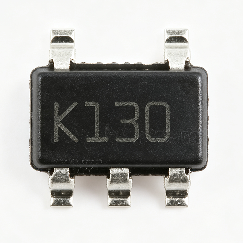
TSV991ILT - 20MHz Rail-to-Rail Op Amp | STMicroelectronics
The STMicroelectronics TSV991ILT is a single, high-speed, rail-to-rail input/output operational amplifier offering a gain-bandwidth product of 20 MHz and a slew rate of 10 V/µs. It operates from a supply voltage range of 2.5 V to 5.5 V, making it suitable for battery-powered and low-voltage applications. The device is available in the compact SOT-23-5 package, ideal for space-constrained designs. An operational amplifier (op-amp) is a high-gain voltage amplifier with differential inputs and a single-ended output. It is a fundamental building block in analog electronics, used in signal conditioning, filtering, and amplification. The TSV991ILT belongs to the family of general-purpose op-amps, which are characterized by their versatility and ease of use. In the hierarchy of analog components, op-amps are part of the broader category of linear integrated circuits, which also includes comparators and voltage regulators. Key features of the TSV991ILT include rail-to-rail input and output stages, which maximize the dynamic range in low-voltage applications. The device also features a low input offset voltage of 1.5 mV (max) and a low input bias current of 1 pA (typ), ensuring high accuracy in precision circuits. The 20 MHz bandwidth and 10 V/µs slew rate enable the amplifier to handle high-frequency signals, making it suitable for video and communication applications. The TSV991ILT is built on STMicroelectronics' advanced BiCMOS process, which combines the benefits of bipolar and CMOS technologies. This process achieves a good balance between speed, power consumption, and noise performance. The amplifier's quiescent current is typically 1.1 mA, providing a favorable trade-off between speed and power efficiency for battery-operated devices. Typical applications include active filters, signal conditioning, portable instrumentation, and audio processing. The rail-to-rail output capability allows the amplifier to drive ADC inputs directly, maximizing the usable input range. In sensor interfaces, the low input bias current minimizes errors when interfacing with high-impedance sensors. When designing with the TSV991ILT, ensure proper power supply decoupling with a 0.1 µF ceramic capacitor placed close to the VCC pin. The input common-mode voltage range extends beyond the supply rails, but care should be taken to avoid exceeding the absolute maximum ratings. The output can swing within 50 mV of the rails, which is beneficial for single-supply operation. This page synthesizes distributor pricing, drop-in alternatives, and practical design notes not found in the STMicroelectronics datasheet, providing a comprehensive resource for engineers evaluating the TSV991ILT.