Amplifier ICs
Products (142)

ADA4941-1ARZ-RL7 - Differential ADC Driver | Analog Devices
The ADA4941-1ARZ-RL7 is a low power, single-ended input, differential output amplifier optimized for driving high resolution analog-to-digital converters (ADCs). Manufactured by Analog Devices on their proprietary second-generation eXtra fast complementary bipolar (XFCB) process, this device achieves 18-bit performance on low supply currents. It is configured in an easy-to-use, single-ended-to-differential gain of +2 configuration, making it ideal for driving 16-bit and 18-bit PulSAR ADCs such as the AD7687, AD7690, and AD7691. A differential ADC driver is an amplifier that converts a single-ended input signal into a differential output, which is required by many high-performance ADCs to improve noise immunity and dynamic range. The ADA4941-1 belongs to the category of differential amplifiers, which are a subset of operational amplifiers used in signal conditioning chains. These amplifiers are essential in precision data acquisition systems where the ADC's performance depends on the quality of the driving signal. Key features of the ADA4941-1 include ultralow distortion of 120 dBc THD at 10 kHz, low noise enabling 97 dB SNR at 100 kHz with a 4 V p-p output, and extremely low power consumption on a 3 V supply. The device operates from a single supply, simplifying power supply design. Its high input impedance minimizes loading on the source, and the differential output provides the balanced drive required by modern ADCs. Technically, the ADA4941-1 uses a single-ended to differential conversion with a fixed gain of +2, eliminating the need for external gain-setting resistors. The output common-mode voltage is set by an internal reference, ensuring proper ADC input range. The XFCB process provides high speed and low distortion while maintaining low power, making it suitable for battery-powered and portable instrumentation. Typical applications include driving 16-bit and 18-bit SAR ADCs in medical imaging, industrial process control, and precision data acquisition systems. The device is also used in communication systems where high dynamic range is required. Its low power consumption makes it ideal for portable and battery-operated equipment. When designing with the ADA4941-1, ensure that the input signal is within the common-mode input range and that the output is properly filtered to avoid aliasing. The device is available in an 8-lead SOIC package, and the RL7 suffix indicates tape and reel packaging for automated assembly.
ADA4945-1ACPZ - Low-Noise FDA ADC Driver | Analog Devices
The ADA4945-1ACPZ is a low-noise, low-distortion, fully differential amplifier (FDA) from Analog Devices, designed for driving high-performance ADCs in data acquisition and signal processing systems. It operates over a broad power supply range of 3 V to 10 V and is available in a compact 16-lead LFCSP (3x3 mm) package. The device features two selectable power modes, allowing designers to trade off power consumption against bandwidth and noise performance, making it highly flexible for a variety of applications. A fully differential amplifier (FDA) is an amplifier with differential inputs and differential outputs, typically used to convert single-ended signals to differential signals or to drive differential-input ADCs. FDAs are essential in high-speed signal chains because they provide common-mode rejection, reduce even-order harmonics, and improve signal integrity by maintaining a balanced signal path. The ADA4945-1 fits into the hierarchy of amplifiers: fully differential amplifier -> differential amplifier -> operational amplifier -> analog IC -> semiconductor. Key features of the ADA4945-1 include low DC offset and offset drift (0.1 µV/°C), excellent dynamic performance, and rail-to-rail output. The device also includes an output common-mode voltage control pin, enabling precise setting of the ADC input common-mode voltage. The two power modes (full power and low power) allow optimization for either maximum bandwidth or reduced power consumption, with a typical quiescent current of [DATA_NEEDED: quiescent current] in full power mode. Technically, the ADA4945-1 uses a high-voltage process to support 10 V operation, which is higher than many competing FDAs. This enables it to drive ADCs with larger input ranges and provides greater headroom. The device also features output limiting, which protects the ADC from overdrive conditions. The low noise and distortion characteristics make it ideal for precision measurement and communications applications. Typical applications include ADC drivers for high-speed data acquisition, medical imaging, communications receivers, and industrial instrumentation. The ADA4945-1 is particularly well-suited for driving ADCs such as the AD9680, AD9268, and AD9656, which are available on XAIPART. Its low offset drift ensures accurate DC performance over temperature, while the rail-to-rail output maximizes dynamic range. When designing with the ADA4945-1, it is important to properly set the output common-mode voltage using the VOCM pin and to select the appropriate power mode for the application. The device requires careful PCB layout to minimize parasitic capacitance and maintain signal integrity. Refer to the ADA4945-1 data sheet for detailed application circuits and layout guidelines.
ADA4945-1ACPZ-RL7 - Low Noise FDA ADC Driver | Analog Devices
The ADA4945-1ACPZ-RL7 from Analog Devices is a low-noise, low-distortion, fully differential amplifier (FDA) designed for driving high-performance ADCs. It operates over a broad power supply range of 3 V to 10 V and features two selectable power modes, allowing designers to optimize between power consumption and dynamic performance. The device is offered in a compact 16-lead LFCSP (3x3 mm) package, making it suitable for space-constrained applications. A fully differential amplifier (FDA) is an amplifier with differential inputs and differential outputs, providing balanced signals that reject common-mode noise and even-order harmonics. FDAs are essential in high-speed signal chains, particularly for driving ADCs, where they convert single-ended signals to differential, provide gain, and buffer the ADC input. The ADA4945-1 fits into the hierarchy: fully differential amplifier -> differential amplifier -> operational amplifier -> analog IC -> semiconductor. Key features include ultra-low DC offset and offset drift (0.1 µV/°C), high speed, and excellent distortion performance. The device achieves low noise and low distortion, making it ideal for data acquisition systems requiring high accuracy. The two power modes allow a trade-off between power dissipation and bandwidth, enabling efficient operation in battery-powered or high-performance systems. Technically, the ADA4945-1 uses a precision architecture with internal common-mode feedback, ensuring accurate output common-mode voltage control. It provides a wide input common-mode range and rail-to-rail output, simplifying interface with various ADC inputs. The device also includes a disable feature for power saving, and its small package minimizes board space. Typical applications include driving high-speed ADCs in communications, instrumentation, and medical imaging systems. It is also used in single-ended to differential conversion, level shifting, and as a buffer for precision references. The low offset drift ensures stable performance over temperature, critical for precision measurement. When designing with the ADA4945-1, ensure proper power supply decoupling with 0.1 µF and 10 µF capacitors close to the pins. The feedback network must be carefully matched to maintain balance and minimize distortion. The device's power mode selection should be based on the required bandwidth and power budget.
ADA4950-1YCPZ - Differential ADC Driver G=1/2/3 | ADI
The ADA4950-1YCPZ is a low power, selectable gain differential ADC driver from Analog Devices, Inc. It provides fixed gains of 1, 2, or 3 using on-chip feedback and gain resistors, eliminating the need for external resistor networks and reducing BOM area. The device is packaged in a 16-lead LFCSP-VQ (3x3 mm) and supports a single supply range of 3 V to 11 V or a dual supply range of ±1.5 V to ±5.5 V. It is designed for driving high performance analog-to-digital converters (ADCs) in both single-ended-to-differential and differential-to-differential configurations. A differential ADC driver is a specialized amplifier that converts a single-ended or differential analog signal into a balanced differential output centered at a desired common-mode voltage, which is essential for driving modern high-speed ADCs. These converters rely on differential inputs to improve common-mode noise rejection, reduce even-order harmonic distortion, and double the dynamic range compared with single-ended driver solutions. Within the signal chain hierarchy, the ADC driver sits between the anti-aliasing filter and the converter input, providing scaling, buffering, and level shifting. Key features of the ADA4950-1 include on-chip gain select pins for G=1, 2, 3, low power consumption enabled by the proprietary silicon-germanium (SiGe) complementary bipolar process, and 114 mA output current per channel. The internal feedback network maintains excellent gain accuracy without external precision resistors, and the low distortion and noise floor suit demanding data acquisition and communications applications. The SiGe complementary bipolar fabrication process provides the ADA4950-1 with a favorable speed-to-power ratio, making it possible to achieve wide bandwidths and low harmonic distortion while consuming less quiescent current than amplifiers built in older bipolar processes. The ADA4950-1 is the single-channel version; the ADA4950-2 is the dual-channel companion for multichannel systems. Typical applications include high-speed ADC input stages in instrumentation, IF sampling and baseband signal chains in software-defined radios, differential buffering for sensors, and ultrasound and radar preprocessing. The 3x3 mm LFCSP package supports compact board layouts. When designing with the ADA4950-1, connect the gain select pins according to the desired closed-loop gain and place 0.1 uF decoupling capacitors as close as possible to the supply pins. The output common-mode voltage must be set within the ADC input range to avoid clipping and preserve converter dynamic performance.
ADA4950-1YCPZ-RL7 - Selectable Gain Diff ADC Driver | Analog Devices
The ADA4950-1YCPZ-RL7 from Analog Devices is a low power, selectable gain differential ADC driver with on-chip feedback and gain resistors. It is a gain-selectable version of the ADA4932-1, offering gains of 1, 2, and 3 without external resistors. The device is housed in a 16-lead LFCSP-VQ (3x3 mm) package and is designed to drive high performance analog-to-digital converters (ADCs) in both single-ended-to-differential and differential-to-differential configurations. A differential amplifier is an electronic amplifier that amplifies the difference between two input voltages while rejecting common-mode signals. In the signal chain hierarchy, a differential ADC driver sits between the sensor or analog front-end and the ADC, converting single-ended signals to differential or buffering differential signals to provide the low impedance, high linearity drive required for high-resolution conversion. This function is critical in applications such as communications, instrumentation, and medical imaging where signal integrity directly impacts system performance. Key features of the ADA4950-1 include selectable gains of 1, 2, and 3 via a single gain pin, eliminating the need for external resistor networks and reducing component count. The device operates from a single 3.3V to 5V supply or dual supplies up to ±5V, and features a wide bandwidth suitable for driving ADCs with sample rates up to 100 MSPS. The low power consumption of 5.5 mA quiescent current makes it ideal for battery-powered and channel-dense systems. The output common-mode voltage is adjustable, allowing direct interface to ADC input ranges. Technically, the ADA4950-1 uses an internal feedback network with precision laser-trimmed resistors to achieve accurate gains and low distortion. The device provides a differential output with a common-mode reference pin (VOCM) that sets the output common-mode level, simplifying ADC interface design. The input voltage noise is 3.5 nV/√Hz, and the spurious-free dynamic range (SFDR) is excellent, ensuring high fidelity signal conversion. The LFCSP package with exposed pad offers good thermal performance and a compact footprint for space-constrained designs. Typical applications include driving high-speed ADCs in communications receivers, medical ultrasound equipment, and test and measurement instruments. The selectable gain feature allows the same board design to accommodate different input signal levels, reducing design time and BOM cost. The device is also suitable for differential signaling over twisted-pair cables in industrial and automotive systems. When designing with the ADA4950-1, ensure proper power supply decoupling with 0.1 µF and 10 µF capacitors close to the supply pins. The VOCM pin should be driven by a low-impedance source to set the output common-mode voltage accurately. The gain select pin (G1) must be tied to the appropriate logic level to achieve the desired gain, and the input pins should be AC-coupled if the source has a DC offset.
ADA4950-2YCPZ - Dual Differential ADC Driver | Analog Devices
The ADA4950-2YCPZ is a dual, gain-selectable differential amplifier from Analog Devices, designed as a high-performance ADC driver. It is a member of the ADA4950 family, which includes the ADA4950-1 (single) and ADA4950-2 (dual) versions. These amplifiers feature on-chip feedback and gain resistors, allowing fixed gains of 1, 2, and 3 without external components. The ADA4950-2 is fabricated using Analog Devices' proprietary silicon-germanium (SiGe) complementary bipolar process, which enables low distortion and low noise at low power consumption. The device operates from a single 3.3V to 11V supply or dual ±1.65V to ±5.5V supplies, and is available in a 24-lead LFCSP (4x4 mm) package. A differential amplifier is an electronic amplifier that amplifies the difference between two input voltages while rejecting common-mode signals. In the context of ADC driving, a differential amplifier converts a single-ended signal to a differential signal or buffers a differential signal, providing the necessary drive strength and level shifting to interface with high-performance analog-to-digital converters. The ADA4950-2 is specifically optimized for this role, offering low noise, low distortion, and high bandwidth to preserve signal integrity. Key features of the ADA4950-2 include a -3 dB bandwidth of 1.35 GHz (gain = 1), a slew rate of 2900 V/µs, and a low input voltage noise of 2.2 nV/√Hz. The device provides a differential output with a common-mode voltage set by an internal reference, simplifying interface to ADCs. It also features a power-down mode to conserve energy when not in use. The on-chip gain resistors eliminate the need for external resistor networks, reducing board space and component count. The ADA4950-2 is well-suited for a wide range of applications, including communications, instrumentation, and medical imaging. Its high bandwidth and low distortion make it ideal for driving high-speed ADCs in software-defined radios, radar systems, and test equipment. The low power consumption (typically 9.5 mA per amplifier) is beneficial for portable and battery-powered devices. When designing with the ADA4950-2, it is important to consider proper power supply decoupling and PCB layout to achieve optimal performance. The exposed pad on the LFCSP package should be soldered to a ground plane for thermal and electrical performance. Additionally, the input common-mode voltage range and output swing should be checked against the ADC's input requirements to ensure proper operation.
ADA4950-2YCPZ-RL7 - Selectable Gain Diff ADC Driver | Analog Devices
The ADA4950-2YCPZ-RL7 is a dual, low power, selectable gain differential ADC driver from Analog Devices. It is a gain-selectable version of the ADA4932-2, featuring on-chip feedback and gain resistors that allow the user to select gains of 1, 2, or 3 without external components. This device is designed to drive high-performance analog-to-digital converters (ADCs) in both single-ended-to-differential and differential-to-differential configurations. Housed in a compact 24-lead LFCSP (4x4 mm) package, it operates from a single 3.3V to 11V supply or dual ±1.65V to ±5.5V supplies, making it versatile for various signal chain designs. A differential ADC driver is a specialized amplifier that converts a single-ended or differential input signal into a balanced differential output, optimized to interface with the differential inputs of high-speed ADCs. It provides the necessary gain, common-mode voltage shifting, and low output impedance to drive the ADC's sampling capacitor without degrading signal integrity. In the signal chain hierarchy, a differential ADC driver sits between the sensor/amplifier stage and the ADC, ensuring that the ADC receives a clean, well-conditioned signal for accurate conversion. Key features of the ADA4950-2 include a wide -3 dB bandwidth of 750 MHz, a slew rate of 2900 V/µs, and a low input voltage noise of 2.2 nV/√Hz. The device also offers a low offset voltage of 200 µV and a high output current of 60 mA, enabling it to drive the capacitive loads of ADCs effectively. The selectable gain feature simplifies design by eliminating the need for external resistor networks, reducing board space and component count. Fabricated using Analog Devices' proprietary silicon-germanium (SiGe) complementary bipolar process, the ADA4950-2 achieves low distortion and noise at low power consumption. The device features a power-down mode that reduces quiescent current to 0.5 mA, making it suitable for power-sensitive applications. Its excellent dynamic performance, including a spurious-free dynamic range (SFDR) of -90 dBc at 10 MHz, ensures high-fidelity signal processing. Typical applications include driving high-speed ADCs in communications, instrumentation, and medical imaging systems. It is also used in single-ended-to-differential conversion for balanced audio and video signals, and in differential signal conditioning for industrial sensors. The ADA4950-2's low power and small footprint make it ideal for portable and battery-powered equipment. When designing with this device, ensure proper power supply decoupling with 0.1 µF and 10 µF capacitors placed close to the VCC and VEE pins. The output common-mode voltage can be set via the VOCM pin, which should be driven by a low-impedance source to maintain accuracy. For optimal performance, keep the feedback and gain paths short and use ground planes to minimize parasitic inductance.
ADL5562ACPZ-R7 - 3.3GHz RF/IF Differential Amplifier | Anal
The Analog Devices ADL5562ACPZ-R7 is a high performance differential amplifier optimized for RF and IF applications. It provides 10 MHz to 3.3 GHz operation, 2.1 nV/√Hz input voltage noise, and pin-strappable gain levels of 6 dB, 12 dB, and 15.5 dB in a 16-lead LFCSP-VQ (3 mm x 3 mm) package. Operating from a 3 V to 3.6 V supply, the device uses a VCOM pin for output common-mode control and is specifically designed to drive high-speed 8-bit to 16-bit ADCs. An RF/IF differential amplifier is a wideband amplifier that takes a balanced or single-ended input and produces a differential output, preserving signal integrity while rejecting common-mode noise. It sits between the IF filter or mixer and the ADC, providing gain and low distortion so that the converter sees a clean, well-conditioned signal. In the amplifier hierarchy, the ADL5562 is an RF/IF-specific differential driver, distinct from general-purpose operational amplifiers or baseband video buffers. Key features include a 3.3 GHz bandwidth for high-IF sampling, 2.1 nV/√Hz input noise for high-SNR receiver chains, and three pin-selectable gain settings that eliminate the need for external gain-setting resistors. The output common-mode is adjustable through the VCOM pin, allowing direct interface to a wide range of ADC input stages. The low noise figure of 7.3 dB at maximum gain is a useful starting point for chain budget analysis. The ADL5562 uses a feed-forward resistor architecture to set gain without external components, simplifying BOM and layout. The amplifier provides high differential open-loop gain and an output common-mode circuit that gives designers flexible dc biasing. The 16-lead LFCSP-VQ package with exposed pad supports good thermal and electrical grounding in compact RF front ends. Typical applications include high-IF ADC drivers for communications receivers, IF sampling in software-defined radio, test and measurement front ends, and broadband instrumentation. The device is also suited for radar and defense IF chains where 3.3 GHz bandwidth and low distortion are required. Its combination of low noise, high bandwidth, and pin-programmable gain makes it a practical building block for modern receiver architectures. When designing with this amplifier, keep the VCOM pin properly bypassed and place gain-select strap resistors or solder bridges close to the device. Follow the datasheet application circuits for input matching, output filtering, and power supply decoupling to achieve the specified distortion and noise performance.
ADUM3190ARWZ-RL7 - 2.5kV Isolated Error Amplifier | Analog Devices
The ADUM3190ARWZ-RL7 is an isolated error amplifier from Analog Devices, based on iCoupler® technology. It is designed for linear feedback power supplies, providing a precise 1.225 V reference and a wide supply range of 3 V to 20 V on both sides. The device offers 400 kHz bandwidth and 2.5 kV rms isolation, making it suitable for isolated power conversion applications. An isolated error amplifier is a specialized amplifier that transfers an error signal across an isolation barrier without a direct electrical connection. It is a key component in isolated power supplies, where it compares the output voltage to a reference and sends the error signal to the primary-side controller. This enables regulation while maintaining galvanic isolation for safety and noise immunity. Key features include a 1.225 V reference voltage, compatibility with Type II or Type III compensation networks, and low power operation of less than 7 mA total. The device supports a wide supply range of 3 V to 20 V on both VDD1 and VDD2, and provides 400 kHz bandwidth. It is available in a 16-lead SOIC-W package, offering a compact solution for isolated feedback. The ADUM3190 uses iCoupler technology, which integrates micro-transformers to achieve isolation, eliminating the need for optocouplers and providing improved reliability and performance. The device is compatible with DOSA (Distributed-power Open Standards Alliance) standards, ensuring interoperability. It also meets safety approvals including UL 1577 and IEC/EN/CSA 62368-1. Typical applications include shunt regulators, linear power supplies, inverters, and uninterruptible power supplies (UPS). The device is ideal for isolated feedback in AC-DC and DC-DC converters, where precise regulation and isolation are critical. Its wide supply range and low power consumption make it suitable for both industrial and consumer power systems. When designing with the ADUM3190, ensure proper PCB layout to maintain isolation creepage and clearance distances. The device requires bypass capacitors on both supply pins to ensure stable operation. The reference voltage accuracy is critical for output regulation, so use precision resistors in the feedback network.
ADUM3191ARWZ-RL7 - Isolated Error Amplifier | Analog Devices
The Analog Devices ADUM3191ARWZ-RL7 is an isolated error amplifier based on iCoupler technology, supplied in a 16-lead SOIC-W (RWZ) tape-and-reel package. It provides precision isolated voltage feedback for linear and switch-mode power supplies without depending on optocoupler current-transfer-ratio drift. The device integrates an error amplifier and a galvanic isolation barrier in one monolithic IC, simplifying PCB layout, reducing component count, and improving long-term stability. An isolated error amplifier is a specialized analog building block that compares a feedback voltage on one side of an isolation barrier with an internal reference and transmits a corrected error signal to the other side across the barrier. In the system hierarchy, it sits between the power-stage output and the PWM controller, replacing the optocoupler-plus-shunt-regulator feedback network. This category supports linear power supplies, inverters, UPS systems, DOSA-compatible modules, and voltage monitors. Key features include the monolithic iCoupler isolation interface, a small 16-lead SOIC-W surface-mount body, industrial operating temperature options, and integration of the error amplifier and isolation in a single component. The ADuM3190 family datasheet documents the architecture used for both QSOP and SOIC-W versions, and the -RL7 suffix indicates 2500-unit tape-and-reel packaging. Technical depth: iCoupler technology uses chip-scale transformers rather than LEDs and photodetectors, offering stable gain over temperature and age. Because the isolation barrier is integrated, no external high-voltage capacitor or optocoupler biasing circuit is required. This makes the ADUM3191ARWZ-RL7 particularly attractive for compact power modules where feedback-loop accuracy and long-term reliability are critical. Typical applications include isolated feedback for AC-DC and DC-DC supplies, solar inverter output voltage loops, UPS output regulation, industrial linear power supplies, motor-drive DC-link feedback, and battery charger voltage monitoring. Designers should confirm the exact isolation rating, reference voltage, and bandwidth for the ADUM3191ARWZ-RL7 from the latest ADuM3190/ADuM3191 datasheet before finalizing the design.
ADUM3195ARWZ - Isolated Amplifier with Adjustable Gain | Analog Devices
The ADUM3195ARWZ is an isolated amplifier with adjustable gain and single-ended output from Analog Devices. It is designed for precision voltage and current sensing in isolated power supply feedback loops, motor control, and industrial automation. The device provides galvanic isolation up to 3000 V rms, ensuring safe signal transfer across isolation barriers. It operates from dual supplies: VDD1 and VDD2, each ranging from 4.5 V to 5.5 V. The bandwidth is 210 kHz, making it suitable for high-speed control loops. The ADUM3195ARWZ comes in a 16-lead SOIC (RW-16) package, offering a compact solution for space-constrained designs. An isolated amplifier is a type of amplifier that provides electrical isolation between its input and output stages, preventing dangerous voltages or ground loops from affecting the signal path. It is a critical component in applications where safety and noise immunity are paramount, such as in medical devices, industrial motor drives, and power conversion systems. The isolation barrier is typically implemented using capacitive or magnetic coupling, allowing signal transfer without a direct electrical connection. This enables the amplifier to measure voltages or currents across a high-voltage boundary while maintaining signal integrity and protecting low-voltage control circuitry. Key features of the ADUM3195ARWZ include adjustable gain, which allows designers to set the amplification factor according to their specific sensing requirements. The single-ended output simplifies interfacing with ADCs and microcontrollers. The device also offers excellent common-mode transient immunity, ensuring reliable operation in noisy industrial environments. The 210 kHz bandwidth supports fast transient response, essential for stable feedback loops in switching power supplies. The wide supply range of 4.5 V to 5.5 V on both sides provides flexibility in system design. Technically, the ADUM3195ARWZ uses Analog Devices' iCoupler technology, which integrates isolation and amplification in a single chip. This technology uses chip-scale transformers to transmit signals across the isolation barrier, offering superior performance compared to optocouplers, including higher speed, lower power consumption, and better reliability. The adjustable gain is implemented via an external resistor network, allowing precise control over the amplification factor. The device also features a reference output, which can be used to set the common-mode voltage of the output signal. Typical applications include isolated voltage sensing in AC-DC and DC-DC converters, current sensing in motor drives, and isolated signal conditioning in industrial process control. The ADUM3195ARWZ is also used in battery management systems and solar inverters, where isolation is required for safety and noise reduction. Its high bandwidth and adjustable gain make it ideal for closed-loop control systems that require accurate and fast feedback. When designing with the ADUM3195ARWZ, it is important to ensure proper decoupling on both supply pins and to place the external gain-setting resistors close to the device to minimize parasitic capacitance. The layout should also maintain adequate creepage and clearance distances on the PCB to meet isolation safety standards.
ADUM3195ARWZ-RL7 - Isolated Amplifier | Analog Devices
The ADuM3195ARWZ-RL7 is an isolation amplifier based on Analog Devices' iCoupler® technology, designed for isolated voltage sensing applications. It features very low offset and gain error, making it ideal for precision isolated feedback in power supplies, motor drives, and industrial control systems. The device provides a single-ended output and adjustable gain, allowing flexible configuration for various sensing ranges. It is available in a 16-lead SOIC-W package, suitable for surface-mount assembly. An isolation amplifier is a type of amplifier that provides electrical isolation between its input and output stages, typically using capacitive or magnetic coupling. This isolation protects sensitive control circuitry from high voltages, ground loops, and noise, while maintaining signal integrity. In the hierarchy of signal conditioning, an isolation amplifier falls under analog front-end components, which are essential in industrial and automotive applications where safety and reliability are paramount. Key features of the ADuM3195 include a wide input common-mode voltage range, high common-mode transient immunity, and low power consumption. The device operates over a wide temperature range, making it suitable for harsh environments. Its adjustable gain allows designers to optimize the output swing for specific ADC inputs, reducing the need for external scaling components. Technically, the ADuM3195 uses iCoupler technology, which employs chip-scale transformers to transmit signals across the isolation barrier. This approach offers advantages over optocouplers, such as higher speed, better reliability, and no LED degradation over time. The device also includes an internal reference and output amplifier, simplifying the external circuit design. Typical applications include isolated voltage sensing in switch-mode power supplies, motor control, and battery monitoring systems. The ADuM3195 is also used in isolated data acquisition systems where ground loop isolation is critical. Its low offset and gain error ensure accurate measurement, which is essential for closed-loop control. When designing with the ADuM3195, it is important to provide proper power supply decoupling and to follow the recommended layout guidelines to maintain isolation performance. The device requires a separate ground plane for the input and output sides to achieve the specified common-mode transient immunity.
ADUM3196ARWZ - Isolated Error Amplifier | Analog Devices
The ADUM3196ARWZ is an isolated error amplifier from Analog Devices, designed for use in isolated power supply feedback loops. It combines a precision error amplifier with an integrated digital isolator, providing a compact solution for voltage regulation across an isolation barrier. The device operates from a single 3.0V to 20V supply on the primary side and supports a secondary-side supply from 3.0V to 20V, making it versatile for various power conversion topologies. An isolated error amplifier is a specialized component that amplifies the difference between a reference voltage and a feedback signal while providing galvanic isolation between the input and output. This isolation is critical in power supplies where the primary and secondary sides must be electrically separated for safety and noise immunity. The ADUM3196ARWZ integrates this function into a single SOIC-16 package, reducing board space and component count compared to discrete solutions. Key features of the ADUM3196ARWZ include a 400 kHz bandwidth, a typical offset voltage of 0.5 mV, and a gain of 1 V/V. The device provides reinforced isolation with a working voltage of 1000 Vrms and a transient immunity of 25 kV/us, ensuring reliable operation in harsh industrial environments. It also features an internal 1.0V reference, simplifying the design of feedback networks. The ADUM3196ARWZ uses Analog Devices' iCoupler technology, which integrates magnetic isolation with analog circuitry on a single chip. This architecture provides precise signal transfer across the isolation barrier without the need for external optocouplers or separate isolation amplifiers. The device is designed for high reliability, with a typical isolation lifetime of 50 years at 1000 Vrms working voltage. Typical applications include isolated DC-DC converters, AC-DC power supplies, and isolated voltage sensing in industrial, automotive, and telecommunications systems. The device is particularly suited for applications requiring high accuracy and stability over temperature, such as server power supplies and battery chargers. When designing with the ADUM3196ARWZ, ensure proper PCB layout to maintain isolation spacing and minimize parasitic capacitance. The device requires a bypass capacitor on both supply pins, and the feedback network should be placed close to the error amplifier inputs to reduce noise pickup.
ADUM3196ARWZ-RL7 - Isolated Error Amplifier | Analog Devices
The ADUM3196ARWZ-RL7 is an isolated error amplifier with adjustable gain and single-ended output from Analog Devices, designed for shunt regulator, linear power supply, inverter, and UPS applications. It integrates Analog Devices' iCoupler technology to provide galvanic isolation between the primary and secondary sides, eliminating the need for optocouplers and improving reliability and performance. The device operates from a 3.0 V to 20 V supply on the primary side and 3.0 V to 20 V on the secondary side, with a typical quiescent current of 1.2 mA. It offers a bandwidth of 200 kHz and a gain accuracy of ±1%, making it suitable for precise voltage and current sensing in isolated power conversion systems. An isolated error amplifier is a specialized amplifier that provides electrical isolation between its input and output while maintaining accurate signal transfer. It is commonly used in isolated power supplies to sense output voltage or current and feed back a control signal across the isolation barrier. The ADUM3196ARWZ-RL7 belongs to the category of isolation amplifiers, which are part of the broader family of analog signal conditioning ICs. These components are essential in applications requiring safety isolation, noise immunity, and ground loop elimination. Key features of the ADUM3196ARWZ-RL7 include a wide input common-mode voltage range of -0.3 V to 20 V, a fixed gain of 1 V/V (adjustable with external resistors), and a high common-mode transient immunity of 25 kV/µs. The device is available in a 16-lead SOIC (RW-16) package, which is compact and suitable for space-constrained designs. It also features an internal reference of 1.2 V and a shutdown pin for power saving. The operating temperature range is -40°C to +125°C, making it suitable for industrial and automotive environments. Technically, the ADUM3196ARWZ-RL7 uses a proprietary iCoupler transformer-based isolation technology, which offers superior performance compared to optocouplers, including higher speed, better temperature stability, and longer lifespan. The device includes an internal voltage reference and an error amplifier with a transconductance output stage, allowing direct connection to a shunt regulator or a PWM controller. The gain can be set externally using two resistors, providing design flexibility. The output is single-ended, simplifying interface with downstream control circuits. Typical applications include isolated voltage sensing in AC-DC power supplies, isolated current sensing in motor drives, and feedback control in solar inverters. The device is also used in battery management systems and industrial automation where galvanic isolation is required. Its high common-mode transient immunity ensures reliable operation in noisy environments. When designing with the ADUM3196ARWZ-RL7, it is important to provide adequate decoupling on both supply pins and to ensure that the isolation barrier is not stressed beyond its rated voltage. The gain-setting resistors should be precision types to maintain accuracy. The device is RoHS compliant and lead-free, meeting environmental standards.
E-TDA7391PDTR - 2x40W Dual BTL Audio Amplifier | STMicroelectronics
The E-TDA7391PDTR is a dual-channel bridge-tied load (BTL) audio power amplifier from STMicroelectronics, designed for high-quality car radio and multimedia applications. It delivers up to 2x40W of output power into a 4-ohm load with a 14.4V supply, making it a robust solution for automotive audio systems. The device is housed in a PowerSO-20 package, which provides excellent thermal performance for high-power operation. An audio power amplifier is an electronic device that increases the amplitude of audio frequency signals to drive loudspeakers. In the hierarchy of audio electronics, a BTL amplifier is a type of linear amplifier that uses a bridge configuration to double the voltage swing across the load, effectively quadrupling the output power compared to a single-ended amplifier with the same supply voltage. This makes BTL amplifiers ideal for automotive applications where the battery voltage is limited to 12V or 14.4V, and high output power is required without using bulky transformers or switching converters. Key features of the E-TDA7391PDTR include a wide operating supply voltage range of 8V to 18V, a low quiescent current of 120mA, and a high output power of 40W per channel at 10% THD. The device also features standby and mute functions for power management, a pop-free turn-on/off sequence, and full short-circuit and thermal protection. The PowerSO-20 package has an exposed pad that enhances heat dissipation, allowing continuous operation at high power levels without external heatsinks in many applications. The E-TDA7391PDTR uses a complementary NPN/PNP output stage with a class-AB biasing scheme, which provides low crossover distortion and high linearity. The device incorporates a sophisticated protection circuitry that includes output short-circuit protection, over-temperature shutdown, and load dump protection, ensuring reliable operation in harsh automotive environments. The standby and mute pins allow for easy system-level power management, reducing power consumption when the audio system is not in use. Typical applications include car radio head units, multimedia systems, and aftermarket audio amplifiers. The high output power and low distortion make it suitable for driving mid-range and subwoofer speakers in automotive sound systems. The device can also be used in home theater systems and portable PA systems where a compact, high-power amplifier is required. When designing with the E-TDA7391PDTR, it is essential to provide adequate power supply decoupling with a 1000uF electrolytic capacitor and a 100nF ceramic capacitor close to the supply pins. The exposed pad must be soldered to a large copper area on the PCB to ensure proper thermal management. Additionally, the standby and mute pins should be controlled with a microcontroller or a simple RC network to ensure a pop-free power-up sequence.
INA214AIDCKR - 26V Bi-Directional Current Sense Amp | TI
The Texas Instruments INA214AIDCKR is a voltage-output, current-shunt monitor (current sense amplifier) that measures current through a shunt resistor across a wide common-mode voltage range of -0.3V to 26V. It is a bi-directional, zero-drift device that provides high accuracy for both high-side and low-side sensing applications. The device is offered in a 6-pin SC-70 (DCK) package, making it ideal for space-constrained designs. A current sense amplifier is a specialized operational amplifier configured to amplify the small differential voltage across a sense resistor while rejecting the common-mode voltage. It is a key building block in power management systems, enabling precise current measurement for overcurrent protection, battery monitoring, and closed-loop control. The INA214 belongs to the INA21x family of current shunt monitors, which are widely used in automotive, industrial, and consumer electronics. Key features of the INA214AIDCKR include a maximum input offset voltage of ±35 µV (for INA210, but the INA214 has ±60 µV per the Xecor comparison), a wide common-mode range, and a bi-directional measurement capability. The device operates from a single 2.7V to 26V supply and draws a low quiescent current, making it suitable for battery-powered applications. The zero-drift architecture ensures minimal offset drift over temperature, enhancing measurement accuracy. The INA214 uses a precision chopper-stabilized amplifier topology that continuously corrects offset and drift, achieving excellent DC accuracy. The output voltage is proportional to the sensed current and can be directly interfaced with ADCs or comparators. The device includes an internal reference for bi-directional operation, allowing measurement of current flow in both directions. Typical applications include overcurrent protection in power supplies, precision current measurement for system optimization, and closed-loop feedback circuits in motor control. The wide common-mode range makes it suitable for high-side sensing in 12V and 24V systems, while the small SC-70 package fits compact PCBs. When designing with the INA214AIDCKR, ensure the shunt resistor is placed appropriately to handle the common-mode voltage and that the output is loaded with a suitable impedance to avoid accuracy degradation. The device is specified for operation from -40°C to +125°C, covering automotive and industrial temperature ranges.

INA219AIDCNR - 26V 12-bit I2C Power Monitor | Texas Instruments
The Texas Instruments INA219AIDCNR is a high-side current shunt and power monitor with an I2C or SMBus-compatible interface, packaged in an 8-pin SOT-23 (DCN) package. It monitors both shunt voltage drop and bus supply voltage, with programmable conversion times and filtering. The device operates from a single 3-V to 5.5-V supply, drawing a maximum of 1 mA of supply current, and senses across shunts on buses that can vary from 0 to 26 V. The INA219 is available in two grades: A and B; the A grade offers an input offset of ±50 µV (max) and an offset drift of ±0.5 µV/°C (max), while the B grade provides higher accuracy and precision. A current shunt monitor is an integrated circuit that measures the voltage drop across a sense resistor placed in series with a load, converting this small differential voltage into a current reading. The INA219 belongs to the family of current sense amplifiers, which are specialized operational amplifiers optimized for high common-mode voltage sensing. In the hierarchy of power management ICs, current shunt monitors sit alongside voltage regulators and battery management ICs, providing essential telemetry for system monitoring and protection. The INA219's bidirectional capability allows it to measure current flowing in both directions, making it ideal for battery charge/discharge monitoring. Key features of the INA219AIDCNR include a 12-bit ADC with programmable gain (0.125, 0.25, 0.5, and 1 V/V), a common-mode voltage range of 0 to 26 V, and an I2C interface with 16 programmable addresses. The device includes a programmable calibration register that enables direct readouts of current in amperes and power in watts, eliminating external scaling calculations. It also features programmable conversion times and averaging to trade off speed versus noise, and an alert pin that can be configured for overcurrent or undervoltage conditions. Technically, the INA219 uses a zero-drift (chopper-stabilized) architecture to achieve low offset and drift, ensuring accurate measurements over temperature. The internal multiplier combines the shunt voltage and bus voltage readings to compute power, reducing host processor overhead. The device supports both I2C and SMBus protocols, with a clock frequency up to 2.56 MHz (SMBus) or 3.4 MHz (I2C fast-mode plus). The SOT-23-8 package is compact, measuring 2.9 mm × 1.6 mm, and is suitable for space-constrained designs. Typical applications include battery chargers, power supplies, and server power monitoring, where accurate current and power measurement is critical for efficiency optimization and protection. The INA219 is also used in automotive and industrial systems for load monitoring and fault detection. Its wide common-mode range and bidirectional sensing make it versatile for both high-side and low-side sensing configurations. When designing with the INA219, ensure the shunt resistor is placed in the high-side path and the device's supply is decoupled with a 0.1 µF capacitor close to the VCC pin. The I2C address pins (A0 and A1) should be tied to VCC or GND to select one of 16 addresses, avoiding conflicts with other devices on the bus.
INA4180AIPWR - 26V Quad Current-Sense Amplifier | TI
The Texas Instruments INA4180AIPWR is a cost-optimized, high-precision quad current-sense amplifier (current-shunt monitor) with four independent voltage-output channels in a 14-pin TSSOP (PW) package. It is part of the INAx180 family, which also includes the single-channel INA180 and dual-channel INA2180. The device senses voltage drops across external current-sense resistors at common-mode voltages from -0.2 V to +26 V, independent of the supply voltage, and provides a rail-to-rail output proportional to load current. The A1 gain option provides 20 V/V gain; other family variants offer 50, 100, or 200 V/V gain. A current-sense amplifier is an analog integrated circuit that amplifies the small differential voltage across a sense resistor (shunt) and translates it to a ground-referenced output voltage or current. In a power management hierarchy, current-sense amplifiers sit between the power path and the monitoring/control stage, providing feedback for overcurrent protection, closed-loop current control, and load telemetry. The INA4180AIPWR integrates four such amplifiers in one IC, reducing component count and board area compared with single or dual devices, while maintaining the cost-optimized architecture of the INAx180 family. Key features include a 350 kHz bandwidth, a common-mode input range from -0.2 V to +26 V, and four independent current-sense channels. The rail-to-rail output stage can drive ADCs, comparators, or microcontrollers directly, and the low-power design makes it suitable for always-on monitoring. The device is offered in industrial-temperature variants and AEC-Q100 qualified Q1 versions (for example, INA4180A2QPWRQ1) for automotive applications. Technically, the INA4180AIPWR integrates matched resistor networks to set the gain with low gain error and good temperature stability. Because the common-mode voltage range is independent of the supply, the amplifier can monitor high-side shunts on a 24 V rail while operating from a low-voltage 3.3 V or 5 V supply. This architecture simplifies level shifting and eliminates the need for a separate high-side supply. Typical applications include industrial motor control, DC-DC converter output current monitoring, battery charging systems, telecom board power monitoring, LED lighting load sensing, and automotive electronic load detection. The 26 V common-mode range and 350 kHz bandwidth provide the headroom and speed needed for transient current measurements in these systems. When designing with the INA4180AIPWR, use precision Kelvin connections to the shunt and keep the input filter resistors close to the IC. Do not exceed the 26 V common-mode limit; add transient protection in industrial or automotive environments.
L9955 - Low Power Quad Operational Amplifier | National Semiconductor (TI)
The L9955 is a low-power quad operational amplifier from National Semiconductor (now part of Texas Instruments), designed for battery-powered and portable applications where low quiescent current is critical. It is offered in a 14-pin DIP or SOIC package, providing four independent op-amps in a single IC. The device operates from a single or dual supply, with a wide supply voltage range that accommodates 3V to 30V single-supply or ±1.5V to ±15V dual-supply configurations. An operational amplifier (op-amp) is a high-gain voltage amplifier with differential inputs and a single-ended output, used in signal conditioning, filtering, and mathematical operations. The L9955 belongs to the category of low-power op-amps, which are optimized for minimal power consumption while maintaining adequate bandwidth and slew rate for general-purpose analog tasks. In the hierarchy of analog ICs, it sits under linear amplifiers, which are part of the broader power management and signal processing IC family. Key features of the L9955 include a low quiescent current of typically 0.4 mA per amplifier, a unity-gain bandwidth of 1 MHz, and a slew rate of 0.5 V/µs. It also offers a wide common-mode input voltage range that includes ground, making it suitable for single-supply operation. The output stage can swing close to the supply rails, maximizing dynamic range in low-voltage systems. These specifications make it an excellent choice for battery monitoring, sensor interfaces, and portable instrumentation. The L9955 uses a bipolar transistor architecture with internal frequency compensation, ensuring stability without external components. The input stage is designed for low offset voltage and low input bias current, which is essential for precision DC applications. The output stage is a class-AB push-pull configuration, providing low crossover distortion and the ability to drive capacitive loads up to 100 pF without oscillation. Typical applications include portable medical devices, battery-powered data loggers, and industrial process control loops. In a battery monitoring circuit, the L9955 can amplify the small voltage drop across a sense resistor, with its low quiescent current extending battery life. For sensor interfaces, the wide input range and rail-to-rail output allow direct connection to ADCs without additional level shifting. When designing with the L9955, ensure proper decoupling of the power supply pins with 0.1 µF ceramic capacitors placed close to the IC. The input common-mode range extends to ground, but for best performance, keep inputs within the specified range. The output can drive loads down to 2 kΩ, but for heavier loads, consider using a buffer stage to maintain linearity.
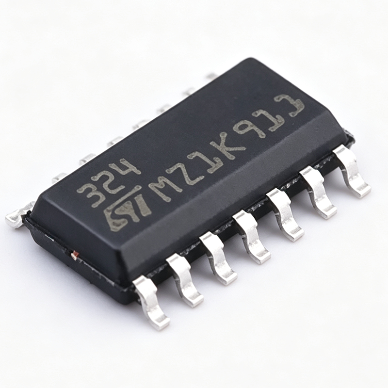
LM324DT - Quad Operational Amplifier | STMicroelectronics
The LM324DT is a quad operational amplifier from STMicroelectronics, featuring four independent, high-gain, internally frequency-compensated op-amps designed to operate from a single power supply over a wide range of voltages. It operates from 3V to 32V (or ±1.5V to ±16V dual supply) and delivers a typical output current of 40mA per channel. The device is housed in a 14-pin SOIC package, making it suitable for space-constrained PCB designs. Data verified as of 2026-08-05. An operational amplifier (op-amp) is a high-gain voltage amplifier with differential inputs and a single-ended output, used in analog signal conditioning, filtering, and mathematical operations. The LM324 is a classic general-purpose op-amp family, known for its low cost, wide supply range, and ability to operate with a single supply, making it a staple in analog electronics. It sits within the hierarchy: operational amplifier -> linear amplifier -> analog IC -> semiconductor. Key features include a wide supply voltage range (3V to 32V), low supply current (typically 700µA per amplifier), common-mode input voltage range including ground, and short-circuit protected outputs. The LM324DT also features true differential input stage, which allows the input to go below ground when operating from a single supply, and it has a typical gain-bandwidth product of 1.3MHz. These features make it versatile for many analog applications. The LM324 uses a bipolar transistor architecture with a class-AB output stage, providing low output saturation voltage and high output current capability. It has an input offset voltage of typically 2mV and input bias current of typically 20nA, which are adequate for many precision applications. The device is internally frequency compensated for unity-gain stability, eliminating the need for external compensation components. Typical applications include transducer amplifiers, DC gain blocks, active filters, and general-purpose signal conditioning in industrial, automotive, and consumer electronics. Its single-supply operation makes it ideal for battery-powered devices and automotive sensor interfaces where a negative rail is not available. When designing with the LM324DT, ensure proper decoupling of the power supply pins with a 0.1µF ceramic capacitor close to the device. The output can swing close to the positive rail but not to the negative rail (ground) when using a single supply, so consider the output voltage range in your design. Also, avoid exceeding the absolute maximum supply voltage of 32V to prevent damage. This page synthesizes distributor pricing, drop-in alternatives, and practical design notes not found in the STMicroelectronics datasheet, providing a comprehensive resource for engineers selecting the LM324DT.
LM358DR - Dual 30V 700kHz Op Amp | Texas Instruments
The LM358DR is a dual operational amplifier from Texas Instruments, housed in an 8-pin SOIC (D) package. It operates from a single supply of 3V to 32V or dual supplies of ±1.5V to ±16V, with a gain bandwidth product of 700 kHz and a slew rate of 0.3 V/µs. This industry-standard device is designed for low power consumption and high gain, making it suitable for a wide range of general-purpose applications. An operational amplifier (op amp) is a high-gain voltage amplifier with differential inputs and a single-ended output. It is a fundamental building block in analog electronics, used in signal conditioning, filtering, and mathematical operations. The LM358 belongs to the family of general-purpose op amps, which are characterized by their versatility, ease of use, and low cost. It is a dual version of the LM321, and the LM324 is its quad counterpart. Key features of the LM358DR include a wide supply voltage range, low quiescent current (typically 500 µA), and the ability to operate with inputs that include ground (single-supply operation). It has internal frequency compensation, short-circuit protection, and a common-mode input range that extends to ground. These features make it ideal for battery-powered devices, sensor interfaces, and industrial control systems. Technically, the LM358 uses a bipolar process and a class-AB output stage, providing low output distortion. It can drive loads as low as 2 kΩ and has a large output voltage swing. The device is specified for the commercial temperature range of 0°C to 70°C. Its low power consumption and wide operating voltage make it a robust choice for many designs. Typical applications include transducer amplifiers, DC gain blocks, active filters, and power supply control circuits. It is also used in portable electronics, automotive sensor interfaces, and test equipment. The LM358DR's SOIC-8 package is surface-mount, suitable for automated assembly. When designing with the LM358DR, ensure proper decoupling of the power supply pins with 0.1 µF capacitors close to the device. Also, consider the output voltage swing limitations when driving loads near the rails. For higher bandwidth or lower noise, consider alternatives like the TL072 or NE5532.
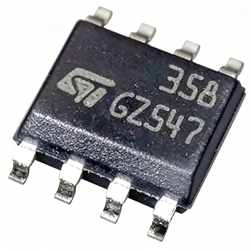
LM358DT - Dual Low Power Op Amp | STMicroelectronics | SOIC-8
The LM358DT is a dual operational amplifier from STMicroelectronics, designed for low-power, general-purpose applications. It operates from a single or split power supply ranging from 3V to 32V (or ±1.5V to ±16V), with a typical quiescent current of 350 µA per amplifier. The device is housed in an 8-pin SOIC (SO-8) package, making it suitable for space-constrained PCB designs. Data verified as of 2026-08-05. An operational amplifier (op-amp) is a high-gain voltage amplifier with differential inputs and a single-ended output. It is a fundamental building block in analog electronics, used for signal conditioning, filtering, and mathematical operations. The LM358 is part of the general-purpose op-amp family, which includes the LM324 (quad version) and LM393 (comparator). These devices are widely used in industrial, automotive, and consumer electronics due to their low cost, ease of use, and wide supply voltage range. Key features of the LM358DT include a wide supply voltage range (3V to 32V), low quiescent current (350 µA per amplifier), and a common-mode input voltage range that includes ground, allowing single-supply operation. The output stage can sink and source current, and the device is short-circuit protected. The LM358DT also features a typical input offset voltage of 2 mV and a gain-bandwidth product of 1.1 MHz, making it suitable for low-frequency signal processing. The LM358DT uses a bipolar transistor architecture with a class-AB output stage, providing low crossover distortion. The input stage is a PNP differential pair, which allows the input common-mode range to extend to the negative supply rail (ground in single-supply operation). This design enables direct sensing of signals near ground, a key advantage in battery-powered and single-supply systems. Typical applications include transducer amplifiers, DC gain blocks, active filters, and signal conditioning in industrial control systems. The LM358DT is also used in portable instrumentation, power supply monitoring, and automotive sensor interfaces. Its low power consumption makes it ideal for battery-operated devices. When designing with the LM358DT, ensure that the input common-mode voltage does not exceed the specified range, and provide adequate decoupling capacitors on the power supply pins. The output can drive loads down to 2 kΩ, but for heavier loads, consider using a buffer stage. The device is stable with capacitive loads up to 500 pF, but for larger loads, an external compensation network may be required. This page synthesizes distributor pricing, drop-in alternatives, and practical design notes not found in the STMicroelectronics datasheet, providing engineers with a comprehensive resource for selecting and using the LM358DT.
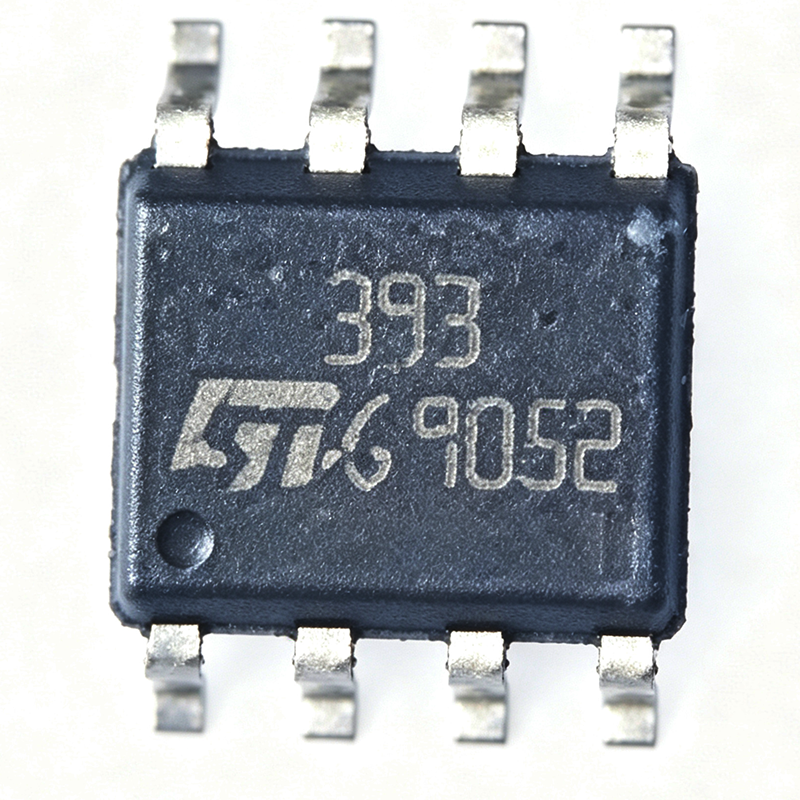
LM393DT - Dual Low-Power Voltage Comparator | STMicroelectronics
The LM393DT is a dual low-power voltage comparator from STMicroelectronics, designed for general-purpose applications requiring precise voltage comparison with minimal power consumption. It operates from a single supply voltage ranging from 2V to 36V or dual supplies from ±1V to ±18V, with a typical supply current of only 0.4 mA per comparator. The device features an open-collector output stage that can sink up to 16 mA, allowing direct interface with TTL, CMOS, and other logic families. The LM393DT is available in the SOIC-8 package, making it suitable for space-constrained PCB designs. Data verified as of 2026-08-05. A voltage comparator is an electronic circuit that compares two input voltages and outputs a digital signal indicating which is higher. The LM393DT is a dual comparator, meaning it contains two independent comparators in a single package. Comparators are fundamental building blocks in analog and mixed-signal systems, used in applications such as threshold detection, zero-crossing detection, and waveform shaping. They are part of the broader category of linear ICs, which also includes operational amplifiers and voltage regulators. The LM393DT's low power consumption and wide supply range make it a versatile choice for battery-powered and industrial applications. Key features of the LM393DT include a low input offset voltage of 2 mV (typical), a low input bias current of 25 nA (typical), and a response time of 1.3 µs (typical) for a 5V overdrive. The open-collector output allows wired-OR connections and level shifting, and the device can operate from a single supply as low as 2V, making it suitable for low-voltage systems. The SOIC-8 package provides a compact footprint with a thermal resistance of 150 °C/W, enabling reliable operation in moderate temperature environments. The LM393DT uses a bipolar transistor architecture with a differential input stage and an open-collector output. This design provides high input impedance and stable operation over a wide temperature range (-40°C to +105°C). The device includes internal ESD protection and is designed to meet JEDEC standards for reliability. The open-collector output requires an external pull-up resistor, which allows the output voltage to be set to any level up to the maximum supply voltage, providing flexibility in interfacing with different logic families. Typical applications for the LM393DT include window comparators, level shifters, oscillator circuits, and analog-to-digital converters. In a window comparator, the dual comparators are used to detect whether an input signal is within a specified voltage range, which is useful in battery monitoring and overvoltage protection. The low power consumption makes it ideal for portable devices, while the wide supply range supports industrial control systems operating from 24V rails. When designing with the LM393DT, ensure that the pull-up resistor is selected to limit the output sink current to within the 16 mA maximum rating. For high-speed applications, minimize parasitic capacitance on the output node to achieve the specified response time. The input common-mode range extends from ground to VCC-1.5V, so ensure that input signals remain within this range for proper operation. This page synthesizes distributor pricing, drop-in alternatives, and practical design notes not found in the STMicroelectronics datasheet, providing a comprehensive resource for engineers selecting and using the LM393DT.
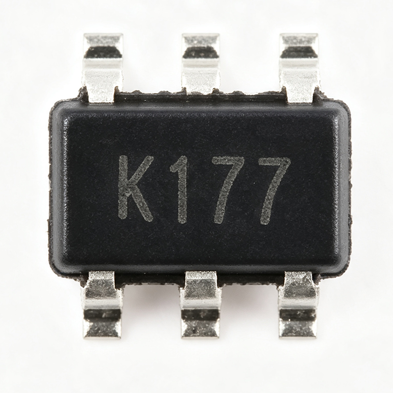
LMV321ILT - Single Low-Power Op Amp | STMicroelectronics
The LMV321ILT is a single, low-power, general-purpose operational amplifier from STMicroelectronics, offered in the compact SOT-23-5 package. It operates from a supply voltage range of 2.7V to 5.5V, making it suitable for battery-powered and portable applications. The device features a typical supply current of 130 µA, a gain-bandwidth product of 1.3 MHz, and an input offset voltage of 1 mV (max). Data verified as of 2026-08-05. An operational amplifier (op-amp) is a high-gain voltage amplifier with differential inputs and a single-ended output. It is a fundamental building block in analog electronics, used in signal conditioning, filtering, and amplification. In the hierarchy of electronic components, an op-amp falls under linear ICs, which are part of the broader category of analog integrated circuits. The LMV321ILT is a low-power variant, optimized for applications where power consumption is critical, such as battery-operated devices. Key features of the LMV321ILT include rail-to-rail input and output stages, which allow the output to swing close to the supply rails, maximizing dynamic range in low-voltage applications. The device also offers a wide operating temperature range of -40°C to +125°C, ensuring reliability in harsh environments. Its low supply current of 130 µA (typical) extends battery life in portable electronics. The LMV321ILT is built on a CMOS process, providing high input impedance and low input bias current. This makes it suitable for interfacing with high-impedance sensors and transducers. The device is unity-gain stable, simplifying design in buffer and follower configurations. Its small SOT-23-5 package is ideal for space-constrained PCB layouts. Typical applications include portable instrumentation, battery-powered signal conditioning, sensor interfaces, and active filters. In portable medical devices, the low power consumption and small footprint are critical. In sensor signal conditioning, the rail-to-rail output ensures maximum signal swing for ADC interfacing. When designing with the LMV321ILT, ensure proper decoupling of the power supply with a 0.1 µF ceramic capacitor placed close to the V+ pin. The input common-mode voltage range includes ground, allowing single-supply operation with ground-referenced inputs. Avoid exceeding the absolute maximum supply voltage of 6V to prevent damage. This page synthesizes distributor pricing, drop-in alternatives, and practical design notes not found in the STMicroelectronics datasheet, providing a comprehensive resource for engineers evaluating the LMV321ILT.