FPGA & CPLD
Products (137)
2VM3104 - Versal Prime Gen 2 Adaptive SoC | AMD | 23x23mm
The AMD 2VM3104 is a Versal Prime Series Gen 2 adaptive SoC designed for space-constrained embedded applications such as Pro AV, broadcast, and industrial IoT. It integrates a quad-core Arm Cortex-A78AE application processing unit (APU) with programmable logic, delivering up to 100K DMIPS of scalar compute in a compact 23 x 23 mm package. This device is part of AMD's second-generation Versal Prime family, which offers up to 10x scalar compute performance compared to previous adaptive SoCs. An adaptive SoC (System-on-Chip) combines a processor subsystem (PS) with programmable logic (PL) on a single device, enabling hardware acceleration and flexible I/O. The Versal Prime Series Gen 2 targets embedded systems requiring high compute density and low latency, bridging the gap between traditional FPGAs and application-specific standard products (ASSPs). The 2VM3104 is positioned as an entry point for customers evaluating the Versal Prime Gen 2 family, with availability expected in 2027. Key features of the 2VM3104 include a quad-core Arm Cortex-A78AE APU with 64 KB L1 cache, a 23 x 23 mm package that is 27% smaller than previous second-generation Versal Prime devices, and higher programmable logic density per square millimeter compared to similarly sized 8-core devices. The device supports up to 100K DMIPS of scalar compute, making it suitable for real-time control and signal processing. Technically, the 2VM3104 leverages AMD's advanced process technology to achieve a balance of power efficiency and performance. The programmable logic fabric allows custom accelerators, while the APU handles general-purpose computing. The compact package enables designs with reduced board area, critical for space-constrained systems. Typical applications include Pro AV equipment (video processing, audio mixing), broadcast infrastructure (encoding, transcoding), and industrial IoT gateways (edge computing, machine vision). The device's small footprint and high compute density make it ideal for these markets. When designing with the 2VM3104, consider thermal management due to the high compute density in a small package. Adequate cooling and power delivery are essential to maintain performance and reliability.

2VM3254 - Versal Prime Gen 2 Adaptive SoC | AMD
The AMD 2VM3254 is a Versal Prime Series Gen 2 adaptive SoC designed for space-constrained embedded applications. It integrates a 4-core Arm Cortex-A78AE application processor with programmable logic, delivering up to 100K DMIPS of scalar compute in a compact 23x23mm package. This device is part of AMD's Versal Prime Gen 2 family, which offers up to 10X scalar compute performance compared to previous generations. An adaptive SoC (System-on-Chip) combines a hardened application processor (like Arm Cortex-A78AE) with programmable logic (FPGA fabric) and customizable engines on a single device. This architecture allows designers to implement both software-defined and hardware-accelerated functions, bridging the gap between traditional microprocessors and FPGAs. The Versal Prime Series Gen 2 targets embedded systems requiring high compute density, low latency, and flexible I/O. Key features of the 2VM3254 include a 23x23mm package (27% smaller than the previous minimum), 4-core Cortex-A78AE processor, and support for Pro AV, broadcast, and industrial IoT applications. The device provides high programmable logic density per square millimeter, enabling complex designs in compact form factors. It also supports the Versal Prime Gen 2 ecosystem, including design tools and early access programs. Technically, the 2VM3254 leverages AMD's adaptive compute acceleration platform (ACAP) architecture, combining scalar engines (Arm cores), adaptable engines (programmable logic), and intelligent engines (AI cores) with a network-on-chip (NoC) interconnect. This heterogeneous architecture allows concurrent execution of software and hardware tasks, optimizing performance per watt for edge applications. Typical applications include Pro AV video processing, broadcast infrastructure, industrial IoT gateways, and edge AI systems. The compact package makes it ideal for space-constrained designs where board area is critical. The device also serves as an entry point for customers evaluating Versal Prime Gen 2 before migrating to larger devices like the 2VM3654. When designing with the 2VM3254, consider the power delivery network (PDN) requirements for the multi-rail SoC, including core, I/O, and memory voltages. Use AMD's power estimation tools and reference designs to optimize decoupling and thermal management in the 23x23mm package.
2VM3358 - Versal Prime Gen 2 Adaptive SoC | AMD
The AMD 2VM3358 is a Versal Prime Series Gen 2 adaptive SoC, featuring 8 Arm Cortex-A78AE application cores and 10 Cortex-R52 real-time cores. This device delivers up to 10x scalar compute compared to previous AMD Versal or Zynq UltraScale+ adaptive SoCs, making it a high-performance heterogeneous computing platform for demanding embedded applications. The 2VM3358 is part of the earliest Versal Prime Gen 2 devices, alongside the 2VM3858 and 2VM3558, and is available in the SFVA1089 package. An adaptive SoC (System-on-Chip) is a heterogeneous computing device that combines programmable logic (FPGA fabric) with hardened processing subsystems, including application processors, real-time processors, and various I/O interfaces. In the Versal architecture, the scalar engines (Cortex-A78AE and Cortex-R52) handle general-purpose and real-time processing, while the programmable logic provides custom hardware acceleration. This hierarchy enables a single device to replace multiple discrete components, reducing system complexity and power consumption. Key features of the 2VM3358 include 8 Arm Cortex-A78AE application cores for high-performance Linux or RTOS applications, 10 Cortex-R52 real-time cores for deterministic, low-latency control tasks, and the Versal adaptive architecture that allows hardware acceleration to be tailored to specific workloads. The device supports up to 10x scalar compute performance versus prior generations, enabling advanced AI, signal processing, and control applications in a single chip. Technically, the 2VM3358 leverages AMD's advanced process technology and the Versal platform's integrated design tools, including Vitis and Vivado. The device's heterogeneous architecture allows developers to partition workloads between scalar processing, programmable logic, and dedicated AI engines (if present in the specific variant). The SFVA1089 package provides a high-density interconnect, supporting high-speed transceivers and memory interfaces for system-level integration. Typical applications for the 2VM3358 include avionics, factory automation, building automation, grid infrastructure, and other industrial or aerospace systems requiring high compute density and real-time responsiveness. The device's combination of scalar performance and programmable logic makes it suitable for edge computing, machine vision, and motor control applications. When designing with the 2VM3358, consider the power consumption of the smallest system configuration, as documented in AMD's support forums. Proper thermal management and power supply design are critical due to the device's high performance and integration level. The SFVA1089 package requires careful PCB layout to manage signal integrity and power distribution.
2VM3454 - Versal Prime Gen 2 Adaptive SoC | AMD
The AMD 2VM3454 is a Versal Prime Series Gen 2 adaptive SoC designed for space-constrained embedded applications such as Pro AV, broadcast, and industrial IoT. It integrates a quad-core Arm Cortex-A78AE application processor, six real-time Arm Cortex-R52 cores, and a Mali-G78AE GPU, delivering up to 100K DMIPS of scalar compute in a compact 23 x 23 mm package. This device is part of AMD's second-generation Versal Prime family, which offers up to 10x scalar compute performance compared to existing adaptive SoCs. An adaptive SoC (System-on-Chip) combines programmable logic (FPGA fabric) with a hardened processor subsystem (PS) and other dedicated engines on a single device. This architecture allows designers to implement custom hardware accelerators in the programmable logic while running complex software on the application cores, bridging the gap between traditional FPGAs and application processors. The Versal Prime Series Gen 2 targets embedded systems requiring high compute density, low latency, and flexible I/O. Key features of the 2VM3454 include the quad-core Cortex-A78AE with 64 KB L1 cache, six Cortex-R52 real-time cores, and a Mali-G78AE GPU. The device is available in a 23 x 23 mm package, enabling compact PCB designs. It supports up to 100K DMIPS of scalar compute, making it suitable for real-time processing and AI inference at the edge. The Versal architecture provides a unified design environment with AMD Vivado and Vitis tools. Technically, the 2VM3454 leverages AMD's advanced 7nm-class process technology, offering a balance of performance and power efficiency. The programmable logic fabric supports high-speed transceivers and flexible I/O standards, while the processor subsystem handles complex control and data processing tasks. The device includes integrated security features and supports functional safety for industrial and automotive applications. Typical applications include Pro AV video processing, broadcast infrastructure, industrial IoT gateways, and edge AI systems. The compact package and high compute density make it ideal for space-constrained designs where performance and power efficiency are critical. When designing with the 2VM3454, consider the power delivery network and thermal management. The device requires multiple voltage rails and adequate decoupling. Use the AMD power estimator tool to calculate power consumption and design the thermal solution accordingly.
2VM3558 - Versal Prime Gen2 Adaptive SoC | AMD
The AMD 2VM3558 is a Versal Prime Series Gen 2 Adaptive SoC, part of the second-generation Versal family that integrates Arm Cortex-A78AE application processors, Cortex-R52 real-time processors, and programmable logic in a single device. It is designed for high-performance embedded applications requiring up to 10x scalar compute compared to previous Versal or Zynq UltraScale+ devices. The 2VM3558 is available in the SSVA1440 package, offering a balance of logic density, I/O, and transceiver capabilities for mid-range designs. An Adaptive SoC is a heterogeneous computing platform that combines scalar processing (Arm cores), adaptable hardware (FPGA fabric), and intelligent engines (DSP, AI) on a single chip. This architecture allows hardware acceleration to be customized post-manufacturing, enabling performance and efficiency gains over fixed-function SoCs. The Versal Prime Gen2 series targets embedded systems where flexibility, performance, and long-term adaptability are critical. Key features of the 2VM3558 include 8 Arm Cortex-A78AE application cores and 10 Cortex-R52 real-time cores, delivering up to 10x scalar compute versus prior generations. It supports PCIe Gen5, 4GB LPDDR5x memory, and GTYP transceivers up to 32Gbps, making it suitable for high-bandwidth data movement. The device also includes a Video Codec Unit and Image Signal Processor, enabling advanced media processing. With up to 1188K logic cells and 543K LUTs, it provides substantial programmable logic resources. Technically, the 2VM3558 leverages AMD's 7nm process technology and advanced packaging to integrate multiple dies, including the programmable logic, processing system, and transceivers. The SSVA1440 package offers a high pin count for extensive I/O and memory interfaces. The device supports industrial temperature ranges (-40°C to +85°C) and is designed for reliability in harsh environments. Typical applications include avionics, defense, industrial automation, and edge computing, where the combination of high-performance scalar processing and adaptable hardware is essential. The 2VM3558 is also used in system-on-modules (SoMs) for rapid prototyping and deployment. When designing with the 2VM3558, consider power delivery complexity: the device requires multiple voltage rails (e.g., 0.85V core, 1.8V I/O) and careful sequencing. Use AMD's power management reference designs and ensure adequate decoupling for high-speed transceivers.
5962-9851001NTB - Military FPGA, 22K Gates | AMD Xilinx
The 5962-9851001NTB is a high-performance Field Programmable Gate Array (FPGA) from AMD Xilinx, designed for demanding aerospace and defense applications. It features 1296 Configurable Logic Blocks (CLBs) and an equivalent gate count of 22,000, with a maximum usable gate count of 65,000. The device is packaged in a 240-pin FQFP (Fine-pitch Quad Flat Package) with gull-wing terminals, and operates over the full military temperature range of -55°C to +125°C. An FPGA (Field Programmable Gate Array) is an integrated circuit that can be configured by the customer after manufacturing to implement any digital logic function. FPGAs belong to the programmable logic device (PLD) family, which sits between fixed-function ASICs and general-purpose processors in the digital logic hierarchy. They offer reconfigurability, parallel processing, and rapid prototyping capabilities, making them essential in applications where flexibility and time-to-market are critical. Key features of the 5962-9851001NTB include its military temperature grade, high-reliability qualification to MIL-PRF-38535 QML, and a maximum clock frequency of 166 MHz. The device provides 3078 logic cells and supports a wide range of I/O standards, enabling integration with various system interfaces. The FQFP package offers a compact footprint with 0.5 mm pitch, suitable for space-constrained military electronics. Technically, the 5962-9851001NTB is based on Xilinx's mature FPGA architecture, featuring a sea-of-gates structure with configurable logic blocks interconnected by programmable routing. This architecture allows designers to implement complex digital systems, including state machines, DSP functions, and communication protocols. The device is supported by Xilinx's ISE design suite, which provides synthesis, place-and-route, and bitstream generation tools. Typical applications include military avionics, satellite communication systems, radar signal processing, and secure communication equipment. Its high reliability and extended temperature range make it suitable for harsh environments where commercial-grade components would fail. When designing with this FPGA, careful attention must be paid to power supply decoupling and signal integrity, as the high-speed I/O and internal logic can generate significant switching noise. Proper PCB layout with multiple ground planes and bypass capacitors is essential for reliable operation.
VM2152 - Versal Prime Adaptive SoC, 757K Logic Cells | AMD
The AMD VM2152 is a mid-range adaptive SoC from the Versal Prime series, integrating dual-core ARM Cortex-A72 application processors and dual-core ARM Cortex-R5F real-time processors with programmable logic. It features 757K logic cells, 112 Gb/s GTM transceivers, and support for high-bandwidth DDR memory interfaces including LPDDR5 up to 6400 Mb/s and DDR5 up to 5600 Mb/s. The device is available in a 1369-FCBGA package (35x35 mm) and operates at processor speeds up to 1.4 GHz for the A72 cores and 600 MHz for the R5F cores. An adaptive SoC (System-on-Chip) combines a processing system (PS) with programmable logic (PL) on a single die, enabling hardware-software co-design and dynamic reconfiguration. The Versal Prime series is the foundational family of AMD's adaptive compute acceleration platform (ACAP), targeting applications that require high data throughput, low latency, and flexibility. The VM2152 specifically uses the Processing System Wizard IP instead of the CIPS IP for configuring the processing system, a unique feature among Versal Prime devices. Key features of the VM2152 include 112 Gb/s GTM transceivers supporting 600 GbE networking, increased DSP capability compared to previous Versal Prime devices, and support for LPDDR5/DDR5 memory interfaces. The device also integrates a programmable network-on-chip (NoC) for efficient data movement between the PS, PL, and memory interfaces. These features make it suitable for high-speed connectivity, data center networking, and wired communications. From a technical perspective, the VM2152 leverages AMD's 7nm process technology, offering a balance of performance and power efficiency. The dual-core A72 cluster provides high-performance general-purpose computing, while the R5F cores handle real-time tasks. The programmable logic fabric supports custom accelerators and protocol implementations, and the integrated NoC simplifies system integration by providing a standardized interconnect. Typical applications include data center networking (600 GbE switches), storage controllers, wired communications (400G connectivity), and high-performance embedded computing. The device's high-bandwidth memory interfaces and transceivers enable it to handle massive data streams with low latency. When designing with the VM2152, careful attention must be paid to power delivery and thermal management due to its high performance. The 1369-FCBGA package requires a robust PCB layout with adequate decoupling and thermal vias. Additionally, the Processing System Wizard IP should be used for PS configuration, as the traditional CIPS IP is not supported on this device.
XA2S200E-6FT256I - 200K Gate FPGA | AMD | 256-FTBGA
The AMD XA2S200E-6FT256I is a member of the Spartan-IIE XA family of Field Programmable Gate Arrays (FPGAs), designed for automotive and industrial applications requiring high performance, abundant logic resources, and a rich feature set at a low cost. This device provides 200,000 system gates, 5,292 logic cells, and 1,176 Configurable Logic Blocks (CLBs), operating from a nominal 1.8V supply. It is housed in a 256-ball FTBGA (17x17 mm) package with 182 user I/O pins. An FPGA (Field Programmable Gate Array) is an integrated circuit that can be configured by the customer or designer after manufacturing—hence "field-programmable." FPGAs are part of the broader programmable logic device (PLD) family, which sits above ASICs in flexibility but below them in unit cost at high volume. The Spartan-IIE family is a superior alternative to mask-programmed ASICs, avoiding the initial cost, lengthy development cycles, and inherent risk of conventional ASICs. FPGA programmability permits design upgrades in the field with no hardware replacement necessary. Key features of the XA2S200E-6FT256I include 57,344 total RAM bits, support for 1.71V to 1.89V supply voltage, and a -40°C to 100°C junction temperature range. The device uses a 0.15-micron CMOS process and supports I/O standards including LVCMOS, LVTTL, and HSTL. The -6 speed grade indicates a maximum internal clock frequency of approximately 200 MHz, suitable for moderate-speed control and data processing tasks. Technically, the Spartan-IIE architecture combines a configurable logic fabric with block RAM and dedicated routing resources. The 256-ball FTBGA package provides excellent thermal and electrical performance, with a compact 17x17 mm footprint. The device is lead-free and RoHS compliant, meeting modern environmental standards. Typical applications include automotive infotainment, motor control, industrial networking, and test equipment. The 182 I/O pins allow flexible interfacing with sensors, ADCs, and communication transceivers. The wide temperature range and automotive qualification make it suitable for under-hood and harsh-environment deployments. When designing with this FPGA, ensure adequate decoupling on the 1.8V core supply and separate I/O supply rails. The device is now obsolete (EOL), so plan for last-time buy or consider pin-compatible alternatives for new designs.
XA3S1000-4FTG256Q - 1M Gate Automotive FPGA | AMD Xilinx
The AMD Xilinx XA3S1000-4FTG256Q is an automotive-grade Field Programmable Gate Array (FPGA) from the Spartan-3 XA family, designed for high-volume, cost-sensitive automotive electronic applications. It delivers 1,000,000 system gates, 17,280 logic cells, and 442,368 total RAM bits in a 256-ball FTBGA package. This device operates with a nominal supply voltage of 1.2V (range 1.14V to 1.26V) and supports 173 user I/O pins, making it suitable for a wide range of automotive control and interface tasks. An FPGA (Field Programmable Gate Array) is an integrated circuit that can be configured by the customer or designer after manufacturing. Unlike fixed-function ASICs, FPGAs contain an array of programmable logic blocks and a hierarchy of reconfigurable interconnects that allow the hardware to be reprogrammed to perform any digital logic function. The Spartan-3 XA family is specifically optimized for automotive applications, meeting the rigorous AEC-Q100 qualification standard for reliability across extended temperature ranges (-40°C to +125°C). Key features of the XA3S1000-4FTG256Q include its automotive qualification (AEC-Q100), 173 user I/O pins, 1920 Configurable Logic Blocks (CLBs), and 442,368 total RAM bits. The device is built on 90nm technology and supports a maximum operating frequency of 125MHz. The FTG256 package (256-ball FTBGA) provides a compact footprint suitable for space-constrained automotive PCBs while offering adequate thermal performance for the device's power dissipation. From a technical architecture perspective, the Spartan-3 XA family uses a 90nm process technology with a 1.2V core voltage, enabling low power consumption while maintaining high logic density. The device includes dedicated multipliers, block RAM, and digital clock managers (DCMs) that support complex digital designs. The automotive-grade variant ensures operation across the full -40°C to +125°C temperature range, making it reliable for under-hood and in-cabin automotive electronics. Typical applications include automotive infotainment systems, engine control units (ECUs), advanced driver-assistance systems (ADAS), and industrial motor control. The device's 173 I/O pins and 1M gate capacity make it ideal for glue logic, sensor interfacing, and display control in automotive environments. When designing with this device, ensure proper power supply decoupling with 0.1uF and 10uF capacitors placed close to the VCC pins. The 1.2V core supply must be clean and stable; consider using a dedicated LDO or DC-DC converter with adequate ripple rejection to maintain reliable FPGA operation.
XA7A12T-1CPG238I - Automotive Artix-7 FPGA | AMD
The AMD XA7A12T-1CPG238I is an automotive-qualified Artix-7 XA Field Programmable Gate Array (FPGA) with 12,800 logic cells, 737,280 bits of block RAM, and 112 user configurable I/O pins. It is supplied in a 238-ball LFBGA/CSPBGA (CSBGA-238) package with a -1 speed grade and is designed for cost-sensitive automotive and industrial applications where low power, small footprint, and reprogrammable hardware logic are essential. An FPGA (Field Programmable Gate Array) is a semiconductor device containing a matrix of configurable logic blocks connected through programmable interconnects; the array can be reprogrammed in the field to implement user-defined digital logic circuits. FPGAs sit between fixed-function ASICs and software processors in the digital system hierarchy, giving engineers the ability to iterate hardware designs without silicon respin. The Artix-7 XA family is specifically screened for automotive quality, bringing FPGA flexibility to vehicle systems. Key features of the XA7A12T-1CPG238I include 12,800 logic elements, 737,280 total block RAM bits, and 112 user I/O in a compact 238-ball CSPBGA. The -1 speed grade offers an entry-level performance point that minimizes cost and power while supporting moderate clock rates for control, interface, and image-processing tasks. The device is RoHS compliant per LCSC listing, and the XA prefix indicates automotive-grade screening. Architecturally, Artix-7 devices integrate a high-performance programmable logic fabric, embedded block RAM, and DSP slices for arithmetic operations. The 737,280-bit block RAM supports distributed FIFOs and line buffers, while the flexible I/O cells connect to a wide range of single-ended and differential signalling standards. These capabilities enable deterministic hardware processing in ADAS, motor control, display bridging, and industrial logic applications. Typical applications include automotive ADAS sensor fusion, electric pump and fan motor control, industrial machine vision, in-vehicle display bridges, battery management safety logic, and UAV flight controllers. The 112 I/O and automotive qualification make the XA7A12T suitable for replacing multiple discrete logic and microcontroller tasks with one programmable device. When designing with the XA7A12T-1CPG238I, pay careful attention to multi-rail power sequencing requirements and the exact CPG238 pinout file. Multiple supply rails, BGA decoupling, and configuration flash selection are critical for first-pass success.
XA7A12T-2CSG325I - Automotive Artix-7 FPGA 12.8K LC | AMD
The AMD Xilinx XA7A12T-2CSG325I is an automotive-qualified Artix-7 field programmable gate array (FPGA) in a 324-ball LFBGA/CSPBGA (CSG325) package. It provides 12,800 logic cells, 150 user I/O, and 737,280 bits of block RAM, with a -2 speed grade that supports high-performance, real-time processing in harsh environments. As part of the XA Artix-7 automotive family, this device delivers AEC-Q100-grade dependability and operates over an industrial temperature range. An FPGA (field-programmable gate array) is a semiconductor integrated circuit whose logic fabric can be configured after manufacturing using hardware description languages such as Verilog or VHDL. FPGAs occupy a unique position in the programmable logic hierarchy, combining hardware-level parallelism with reconfigurability and low-latency I/O. The Artix-7 architecture targets power-conscious, high-volume applications that need moderate logic density, rich I/O flexibility, and deterministic timing. Key feature highlights include 40 DSP48E1 slices for high-throughput multiply-accumulate signal processing, three clock management tiles (CMTs), and a 1.0 V core supply that reduces dynamic power. The -2 speed grade is ideal for 100-300 MHz interface and logic designs. The CSG325 package measures only 15 x 15 mm, with a 0.8 mm ball pitch that allows cost-effective 4-layer PCB routing. The device is JESD-609 e1 lead-free (SnAgCu finish), RoHS compliant, and MSL-3 rated with a 260 C peak reflow temperature. Architecturally, the device uses the proven 7-series SRAM-based fabric with 6-input LUTs, dual flip-flops per slice, and cascade chains for arithmetic. The internal block RAM can be configured as 36 Kb or 18 Kb primitives with multiple parity bits. The configuration engine supports master SPI, master BPI, slave SelectMAP, slave serial, and JTAG modes, providing flexible boot options for automotive and industrial systems. Typical applications are automotive ADAS pre-processing, sensor fusion gateways, industrial motor control, medical ultrasound front ends, networking line cards, broadcast video interfaces, and test equipment. The 150 user I/O with HR (high-range, 1.2 V to 3.3 V) capability lets designers interface directly to many sensors, ADCs, and memory devices without external level shifters. When designing with this device, follow AMD/Xilinx UG583 recommendations for BGA power decoupling: place 1.0 uF and 0.1 uF capacitors under the package on VCCINT, and ensure a monotonic, sequenced power-up of VCCINT, VCCBRAM, and VCCO for reliable configuration.
XA7S25-1CSGA324I - Spartan-7 FPGA, 150 I/O | AMD
The AMD XA7S25-1CSGA324I is a member of the Spartan-7 XA family of Field Programmable Gate Arrays (FPGAs), designed for automotive and industrial applications requiring high performance and reliability. It features 23,360 logic cells, 3,650 adaptive logic modules (ALMs), and 1.58 Mbit of block RAM, providing ample resources for moderate-complexity digital designs. The device is housed in a 324-ball CSGA (Chip-Scale BGA) package with 150 user I/O pins, supporting a core voltage of 0.95V to 1.05V and operating over a temperature range of -40°C to +100°C. An FPGA (Field Programmable Gate Array) is an integrated circuit that can be configured by the customer or designer after manufacturing—hence "field-programmable." FPGAs consist of an array of programmable logic blocks, interconnects, and I/O blocks, allowing them to implement any digital logic function. They are a subset of programmable logic devices (PLDs) and sit within the broader category of embedded processors and controllers. FPGAs are distinct from microcontrollers and ASICs because they offer reconfigurability, enabling rapid prototyping and in-field updates. Key features of the XA7S25-1CSGA324I include 150 user I/Os, 1.58 Mbit of block RAM, and support for various I/O standards such as LVCMOS, LVDS, and SSTL. The device is AEC-Q100 qualified, making it suitable for automotive electronics. It also supports partial reconfiguration and has built-in security features like AES bitstream encryption. The CSGA-324 package offers a compact footprint with a 0.8mm ball pitch, ideal for space-constrained designs. Technically, the Spartan-7 family is built on a 28nm process, balancing performance and power efficiency. The XA7S25 includes DSP slices for signal processing, clock management tiles (CMT) with PLLs and MMCMs, and high-speed transceivers (though this specific variant does not include GTP transceivers). The device supports configuration via JTAG, SPI, or BPI interfaces, and can be programmed using AMD's Vivado Design Suite. Typical applications include automotive driver assistance systems (ADAS), industrial motor control, machine vision, and communication interfaces. The XA7S25's combination of logic density, I/O count, and automotive qualification makes it ideal for these environments. When designing with this FPGA, ensure proper decoupling of the core and I/O supplies, and follow the layout guidelines in UG475 for the CSGA package. The device requires a 1.0V core supply and 1.8V/2.5V/3.3V I/O supplies, depending on the bank configuration.
XC3S1600EFG400 - Spartan-3E FPGA 1.6M Gates | AMD/Xilinx
The AMD/Xilinx XC3S1600EFG400 is a member of the Spartan-3E family of Field Programmable Gate Arrays (FPGAs), offering a high-density programmable logic solution with 33,192 logic cells and an equivalent gate count of 1,600,000. Housed in a 400-ball FBGA package (FG400), this device provides 304 user I/O pins and 663,552 bits of block RAM, making it suitable for a wide range of digital designs. An FPGA (Field Programmable Gate Array) is an integrated circuit that can be configured by the customer or designer after manufacturing—hence 'field-programmable'. FPGAs consist of an array of programmable logic blocks, interconnects, and I/O blocks, allowing the implementation of complex digital circuits without the need for custom fabrication. They are a subset of programmable logic devices (PLDs) and are widely used in prototyping, low-to-medium volume production, and applications requiring reconfigurability. Key features of the XC3S1600EFG400 include 33,192 logic cells, 663,552 bits of block RAM, and support for a maximum clock frequency of 572 MHz. The device operates from a 1.2V core voltage and is manufactured using advanced CMOS technology. The FG400 package offers 400 balls with a 1.00 mm pitch, providing a compact footprint for space-constrained designs. The Spartan-3E architecture is optimized for high performance and low cost, featuring dedicated multipliers, digital clock managers (DCMs), and support for various I/O standards including LVCMOS, LVTTL, and differential standards. The device also includes configuration support via JTAG, SPI, and SelectMAP interfaces, enabling flexible system integration. Typical applications for the XC3S1600EFG400 include industrial control, automotive infotainment, consumer electronics, and communication systems. Its balance of logic density, I/O count, and cost makes it ideal for bridging ASIC prototyping and production. When designing with this FPGA, careful attention must be paid to power supply decoupling and configuration bitstream storage. The 1.2V core requires stable power, and the configuration data is typically stored in an external SPI flash, which must be selected for compatibility.
XC6SLX100-2CSG484C - 101K Logic FPGA | AMD
The AMD XC6SLX100-2CSG484C is a Spartan-6 LX family Field Programmable Gate Array (FPGA) with 101,261 logic cells, 338 user I/Os, and 4,939,776 RAM bits. The device is housed in a lead-free 484-CSPBGA (19x19 mm, 0.80 mm pitch) surface-mount package and operates from a 1.14V to 1.26V core supply. This configuration delivers a compact, high-density programmable logic solution for commercial-temperature (0C to 85C) systems. What is an FPGA? A Field Programmable Gate Array is an integrated circuit whose logic fabric can be configured after manufacturing to implement arbitrary digital functions. FPGAs sit above CPLDs in capacity and are often used for parallel processing, protocol bridging, and hardware acceleration. In a system hierarchy, the Spartan-6 LX family belongs to programmable logic devices, a subset of integrated circuits, and is widely used in communications, industrial automation, and video processing. Key features of XC6SLX100-2CSG484C include 7,911 CLBs, an internal frequency up to 667 MHz, 338 user configurable I/O pins, and 4,939,776 total block RAM bits. The -2 speed grade balances performance and power for cost-sensitive designs. The 484-ball CSPBGA package provides a 19x19 mm footprint with 0.80 mm pitch, making it suitable for space-constrained PCBs. Beneath the package, the Spartan-6 LX100 uses a 45nm CMOS process technology. This process enables high logic density and low static power, with core voltage around 1.2V. The FPGA includes dedicated clock management tile, DSP slices, and block RAM resources that can be used to build efficient digital signal processing pipelines, soft processors, and high-speed I/O interfaces. Typical applications include industrial automation controllers, telecom line cards, video and image processing, software-defined radio, and ASIC prototyping. The 338 I/O pins and abundant logic cells allow integration of multiple peripheral interfaces and custom processing engines on one device. When paired with DDR3 memory such as MT41K256M16HA-125:E or IS43TR16256AL-125KBL, the FPGA can implement high-bandwidth data buffers and packet processing. When designing with this component, plan the power delivery network carefully for the 1.14V to 1.26V core rail and respect the 0C to 85C junction temperature range. Decouple each supply pin and verify configuration memory selection before layout.
XC6SLX100T-2CSG484I - Spartan-6 FPGA 101K Logic Cells | AMD
The AMD XC6SLX100T-2CSG484I is a member of the Spartan-6 LXT FPGA family, built on a mature 45nm low-power copper process technology. It delivers 101,261 logic cells and 296 user I/O pins in a 484-ball CSBGA package, offering a balance of density, performance, and low power for high-volume applications. The device operates from a 1.2V core supply and supports a wide range of I/O standards. An FPGA (Field-Programmable Gate Array) is an integrated circuit that can be configured by the designer after manufacturing, allowing for custom digital logic implementations. FPGAs sit between ASICs and microprocessors in the design hierarchy, providing reconfigurable hardware acceleration for tasks ranging from protocol bridging to digital signal processing. The Spartan-6 family is optimized for cost-sensitive, high-volume applications where low power and system integration are critical. Key features of the XC6SLX100T-2CSG484I include 4,939,776 bits of block RAM, 268 DSP48A1 slices, and support for high-speed serial transceivers (up to 3.125 Gbps) in the LXT variant. The device also includes a hard PCI Express block, memory controllers, and advanced clock management tiles (CMTs) with PLLs and DCMs. These features enable the implementation of complete system-on-chip designs with minimal external components. From a technical perspective, the Spartan-6 family uses a 45nm process that reduces dynamic power consumption by approximately 50% compared to previous Spartan families. The fabric is based on a 6-input look-up table (LUT) architecture, providing efficient logic utilization. The device supports partial reconfiguration, allowing dynamic updates to logic functions without powering down the system. Typical applications include industrial automation, automotive infotainment, medical imaging, and communications equipment. The 296 I/O pins support various standards including LVCMOS, LVDS, and HSTL, making it suitable for interfacing with a wide range of peripherals and memory devices. When designing with this FPGA, careful attention to power supply decoupling and thermal management is essential. The 1.2V core supply should be regulated with low-noise LDOs or switching converters, and the device's power consumption should be estimated using the Xilinx Power Estimator (XPE) tool to ensure adequate cooling.
XC6SLX100T-3FGG484C - Spartan-6 FPGA 101K Logic Cells | AMD
The AMD XC6SLX100T-3FGG484C is a member of the Spartan-6 LXT family of Field Programmable Gate Arrays (FPGAs), built on a mature 45 nm low-power copper process technology. It delivers 101,261 logic cells, 296 user I/O pins, and 4,939,776 bits of block RAM, all in a 484-ball FBGA package. This device is designed for high-volume applications requiring leading system integration with the lowest total cost, offering half the power consumption of previous Spartan families and faster, more comprehensive connectivity. An FPGA (Field Programmable Gate Array) is an integrated circuit that can be configured by the customer or designer after manufacturing—hence 'field-programmable'. FPGAs are part of the broader category of programmable logic devices (PLDs), which sit between application-specific integrated circuits (ASICs) and general-purpose processors in the semiconductor hierarchy. They consist of an array of programmable logic blocks, interconnects, and I/O blocks, allowing designers to implement custom digital logic circuits without the high NRE costs of ASIC development. FPGAs are widely used in prototyping, aerospace, automotive, industrial, and communications applications where flexibility and time-to-market are critical. Key features of the XC6SLX100T-3FGG484C include 101,261 logic cells, 296 user I/O pins, 4,939,776 bits of block RAM, and support for various I/O standards including LVCMOS, LVDS, and HSTL. The device operates from a 1.2V core voltage and is available in the -3 speed grade, which is the fastest speed grade for this part. The 484-ball FBGA package measures 23x23 mm with a 1.0 mm ball pitch, providing a compact footprint for dense PCB designs. The device also includes advanced clock management tiles (CMTs) with PLLs and DCMs, and supports configuration via JTAG, SPI, and BPI interfaces. From a technical depth perspective, the Spartan-6 family is built on a 45 nm low-power copper process, which balances performance and power efficiency. The LXT variant includes high-speed serial transceivers (up to 3.125 Gbps), PCI Express endpoints, and advanced memory controllers, making it suitable for high-bandwidth applications. The device also features dedicated DSP48A1 slices for digital signal processing, providing up to 180 GMACs of performance. The -3 speed grade offers the highest performance, with maximum clock frequencies typically exceeding 400 MHz for internal logic. Typical applications for the XC6SLX100T-3FGG484C include software-defined radio (SDR), industrial motor control, medical imaging, and high-performance computing acceleration. Its combination of logic density, I/O count, and transceiver capabilities makes it ideal for bridging, protocol conversion, and real-time signal processing tasks. The device is also well-suited for aerospace and defense applications where long-term supply and traceability are required. When designing with this FPGA, careful attention must be paid to power supply decoupling and PCB layout. The core voltage (VCCINT) should be regulated at 1.2V with low-noise LDOs or switching regulators, and each power pin should have a 100 nF ceramic capacitor placed as close as possible. Additionally, the configuration bitstream must be stored in an external SPI flash or programmed via JTAG, and the device supports multi-boot for remote updates.
XC6SLX150T-3FGG484I - Spartan-6 LXT FPGA 147K Logic Cells | AMD
The AMD XC6SLX150T-3FGG484I is a high-performance Field Programmable Gate Array (FPGA) from the Spartan-6 LXT family, built on a 45nm CMOS process technology. It delivers 147,443 logic cells and 23,038 adaptive logic modules (ALMs) in a 484-pin FBGA package with a 19x19 mm body and 0.80 mm pitch. The device operates from a 1.2V core supply and supports up to 296 user I/O pins, making it suitable for high-volume, cost-sensitive applications requiring substantial logic density and I/O flexibility. An FPGA (Field Programmable Gate Array) is a semiconductor device containing a matrix of configurable logic blocks (CLBs) and programmable interconnects that can be programmed after manufacturing to implement arbitrary digital logic functions. FPGAs sit within the broader hierarchy of programmable logic devices (PLDs), which themselves fall under the category of integrated circuits. Unlike fixed-function ASICs, FPGAs offer reconfigurability, enabling rapid prototyping, hardware acceleration, and in-field updates, which is critical for evolving standards and algorithm changes. Key features of the XC6SLX150T-3FGG484I include 4.71 Mbit of embedded block RAM, integrated DSP slices for signal processing, and support for multiple I/O standards including LVCMOS, LVDS, and HSTL. The -3 speed grade provides the highest performance within the Spartan-6 LXT family, with internal clock frequencies up to 667 MHz. The device also includes hardened memory controllers for DDR, DDR2, and DDR3, reducing system cost and design complexity. Technically, the Spartan-6 architecture employs a 45nm low-power copper process with a 1.2V core voltage, balancing performance and power consumption. The device integrates Clock Management Tiles (CMTs) containing DCMs and PLLs for robust clock generation and jitter filtering. The LXT variant adds high-speed serial transceivers (up to 3.125 Gbps) and PCIe endpoints, enabling advanced bridging and serial connectivity applications. Typical applications include automotive infotainment systems, industrial automation controllers, consumer electronics bridging, and high-speed data acquisition. The 296 I/Os and 4.71 Mbit memory make it ideal for video processing, motor control, and protocol conversion. The -3 speed grade ensures timing closure for demanding designs. When designing with this FPGA, careful attention to power supply decoupling is essential. Use multiple 100nF and 10uF capacitors near the VCCINT, VCCAUX, and VCCO pins to minimize noise. Additionally, configure the device's I/O standards to match the external interface voltages to prevent damage and ensure signal integrity.
XC6SLX25-2FGG484I - Spartan-6 FPGA 24051 Cells | AMD
The AMD XC6SLX25-2FGG484I is a Field Programmable Gate Array (FPGA) from the Spartan-6 LX family, built on a mature 45 nm low-power copper process technology. It delivers 24,051 logic cells, 958,464 bits of block RAM, and 266 user I/O pins in a 484-ball FBGA package (23x23 mm, 1 mm pitch). The device operates at a core voltage of 1.2V and supports internal clock frequencies up to 500 MHz, with a -2 speed grade providing a balanced performance-power trade-off. An FPGA is an integrated circuit that can be programmed after manufacturing to implement any digital logic function. FPGAs belong to the programmable logic device (PLD) family, which sits between ASICs and general-purpose processors in the semiconductor hierarchy. They offer reconfigurability, parallel processing, and low non-recurring engineering costs, making them ideal for prototyping, low-to-mid volume production, and applications requiring hardware flexibility. Key features of the XC6SLX25-2FGG484I include 24,051 logic cells, 52 DSP48A1 slices, 958,464 bits of block RAM, and support for multiple I/O standards including LVCMOS, LVDS, and SSTL. The device also features integrated memory controllers, clock management tiles (CMT) with PLL and DCM, and support for PCI Express (in LXT variants). The -2 speed grade offers a balance between performance and power consumption, with a maximum internal frequency of 500 MHz. The Spartan-6 family is designed for high-volume, cost-sensitive applications, offering half the power consumption of previous Spartan families. The 45 nm process technology enables high logic density and low static power. The device includes advanced power management features such as suspend mode and partial reconfiguration support, allowing dynamic power optimization in battery-powered systems. Typical applications include industrial automation, automotive infotainment, medical imaging, communications infrastructure, and video processing. The 484-ball FBGA package provides ample I/O for interfacing with external memory, ADCs, DACs, and high-speed serial transceivers (in LXT variants). The industrial temperature grade (-40°C to +100°C) makes it suitable for harsh environments. When designing with this FPGA, ensure proper decoupling of the 1.2V core supply and 2.5V/3.3V auxiliary supplies. Use the configuration pins (MODE, DONE, PROG_B) for reliable device programming. The device supports multiple configuration modes including Master SPI, Slave SelectMAP, and JTAG, providing flexibility in system design.
XC6SLX25-3FGG484I - Spartan-6 FPGA 24051 Cells | AMD
The AMD XC6SLX25-3FGG484I is a member of the Spartan-6 LX family of Field Programmable Gate Arrays (FPGAs), fabricated using a 45nm CMOS process technology. It features 24,051 logic cells, 1,879 configurable logic blocks (CLBs), and 958,464 total RAM bits, providing a balanced mix of logic density and memory resources for a wide range of digital designs. The device is offered in a 484-ball FBGA package (23x23 mm) with 266 user I/O pins, supporting diverse interface standards and flexible I/O configurations. An FPGA (Field Programmable Gate Array) is an integrated circuit that can be configured by the designer after manufacturing, allowing for custom digital logic implementation. FPGAs belong to the programmable logic device (PLD) family, which sits between fixed-function ASICs and general-purpose processors in terms of flexibility and performance. The Spartan-6 series is optimized for low power and cost-sensitive applications, making it a popular choice for industrial, automotive, and telecommunications systems. Key features of the XC6SLX25-3FGG484I include a speed grade of -3, which is the highest performance grade available for Spartan-6 LX devices, enabling faster clock frequencies and improved timing margins. The device operates from a 1.2V core supply (1.14V to 1.26V range) and supports multiple I/O standards, including LVCMOS, LVDS, and HSTL. It also includes dedicated DSP48A1 slices and block RAM for efficient implementation of arithmetic and memory-intensive functions. From a technical perspective, the Spartan-6 architecture incorporates a 6-input look-up table (LUT) fabric, advanced clock management tiles (CMTs) with PLLs and DCMs, and high-speed serial transceivers (in LXT variants). The -3 speed grade provides a maximum internal frequency of 500 MHz, as noted in the datasheet, enabling high-throughput designs. The device is RoHS compliant and lead-free, meeting modern environmental standards. Typical applications for the XC6SLX25-3FGG484I include industrial automation, telecommunications infrastructure, automotive electronics, and video/image processing. Its combination of logic density, I/O count, and low power consumption makes it suitable for bridging, protocol conversion, and real-time control tasks. When designing with this FPGA, careful attention must be paid to power supply decoupling and PCB layout to ensure signal integrity at high speeds. The device requires multiple supply rails (VCCINT, VCCAUX, VCCO) and proper sequencing during power-up. Refer to the Spartan-6 FPGA datasheet and PCB design guidelines for detailed recommendations.
XC6SLX25-N3CSG324C - Spartan-6 FPGA, 24051 Cells | AMD
The AMD XC6SLX25-N3CSG324C is a member of the Spartan-6 LX family of Field Programmable Gate Arrays (FPGAs), designed for high-volume, cost-sensitive applications that require leading system integration capabilities. This device features 24,051 logic cells, 226 user I/O pins, and 958,464 total RAM bits, all housed in a 324-ball CSBGA (Chip-Scale Ball Grid Array) package. Operating from a 1.2V core supply, the XC6SLX25-N3CSG324C is fabricated using a 45nm process technology, balancing performance with power efficiency. An FPGA (Field Programmable Gate Array) is an integrated circuit that can be programmed after manufacturing to implement any digital logic function. FPGAs consist of configurable logic blocks (CLBs), programmable interconnects, and I/O blocks, allowing designers to create custom hardware without the cost and lead time of ASIC development. The Spartan-6 family sits within the broader FPGA hierarchy, positioned as a cost-optimized line below the higher-performance Virtex and Kintex families, making it ideal for applications where price and power are critical. Key features of the XC6SLX25-N3CSG324C include 1,879 CLBs, 38 DSP48A1 slices for digital signal processing, and support for a wide range of I/O standards through SelectIO technology. The device also includes enhanced mixed-mode clock management (MMCM) blocks for precise clock generation, and supports configuration via JTAG, SPI, and BPI interfaces. With a junction temperature range of 0°C to 85°C, this commercial-grade FPGA is suitable for typical industrial and consumer environments. The Spartan-6 architecture incorporates advanced power management modes, including suspend and hibernate states, to reduce static power consumption. The 45nm process technology enables high logic density while maintaining low dynamic power, making the XC6SLX25-N3CSG324C an energy-efficient choice for battery-powered or thermally constrained designs. Additionally, the device supports AES bitstream encryption and Device DNA protection for enhanced IP security. Typical applications for the XC6SLX25-N3CSG324C include motor control, industrial networking, video processing, and software-defined radio. Its 226 I/O pins and 324-ball package provide ample connectivity for interfacing with sensors, ADCs, DACs, and communication transceivers. The FPGA's reconfigurability allows for rapid prototyping and field updates, reducing time-to-market. When designing with this FPGA, careful attention must be paid to power supply decoupling and PCB layout to ensure signal integrity at high I/O speeds. The device requires a 1.2V core supply and 2.5V/3.3V auxiliary supplies, with proper sequencing as specified in the datasheet. Thermal management is also important, as the CSBGA package has a thermal resistance that must be considered for high-utilization designs.
XC6SLX75T-2CSG484C - Spartan-6 FPGA 74,637 LEs | AMD
The AMD XC6SLX75T-2CSG484C is a Field Programmable Gate Array (FPGA) from the Spartan-6 LXT family, built on a mature 45 nm low-power copper process technology. It delivers 74,637 logic cells, 3,170,304 total RAM bits, and 292 user I/O pins in a 484-pin CSBGA (19x19 mm) package. Operating from a 1.2V core supply (1.14V to 1.26V range), this device is designed for high-volume applications requiring leading system integration at the lowest total cost. An FPGA (Field Programmable Gate Array) is an integrated circuit that can be configured by the customer or designer after manufacturing. Unlike fixed-function ASICs, FPGAs contain an array of programmable logic blocks, interconnects, and I/O blocks that can be programmed to implement any digital logic function. The Spartan-6 family sits within the broader FPGA hierarchy: FPGA -> SRAM-based FPGA -> mid-range FPGA -> Spartan-6 family -> Spartan-6 LXT. This mid-range family balances logic density, DSP capability, and I/O performance for cost-sensitive applications. Key features of the XC6SLX75T-2CSG484C include 74,637 logic cells, 3,170,304 RAM bits, 292 user I/O pins, and support for multiple I/O standards including LVCMOS, LVDS, and HSTL. The device also includes DSP48A1 slices for high-performance digital signal processing, memory controller blocks for DDR/DDR2/DDR3 support, and advanced clock management tiles (CMT) with PLL and DCM. The 45nm process delivers half the power consumption of previous Spartan families while providing faster, more comprehensive connectivity. Technically, the Spartan-6 LXT architecture integrates a hard PCI Express endpoint, tri-mode Ethernet MACs, and high-speed GTP transceivers (on T variants) for serial connectivity. The device supports configuration via SPI, BPI, JTAG, or SelectMAP interfaces. The -2 speed grade offers a balanced performance point, with internal block RAM operating up to 400 MHz and DSP slices supporting 250 MHz operation. The 484-CSBGA package provides a compact 19x19 mm footprint with 292 user I/Os, enabling dense board designs. Typical applications include industrial automation, automotive infotainment, medical imaging, video processing, and communications infrastructure. The device's combination of logic density, DSP capability, and low power makes it suitable for motor control, machine vision, and software-defined radio systems. The 1.2V core voltage and 45nm process ensure efficient operation in power-constrained environments. When designing with this device, ensure adequate decoupling on the 1.2V core supply and 2.5V/3.3V auxiliary rails. Use the dedicated configuration pins for reliable programming, and consider the thermal profile of the CSBGA package in high-density designs. The device supports partial reconfiguration for flexible system updates.
XC7A100T - Artix-7 FPGA 101K Logic Cells | AMD
The AMD XC7A100T is a member of the Artix-7 family of Field Programmable Gate Arrays (FPGAs), built on a 28nm process to deliver the lowest power and cost while providing high performance per watt. It features 101,440 logic cells, 15,850 slices, 4,860 Kb of block RAM, 240 DSP48E1 slices, and 6 CMTs (Clock Management Tiles). The device supports up to 210 user I/O pins in the CSG324 package, with 3.3V I/O compatibility and multiple I/O standards including LVCMOS, LVDS, and HSTL. The XC7A100T is available in various speed grades (-1, -2, -3) and temperature ranges (C: 0°C to 85°C, I: -40°C to 100°C), with package options including CSG324, FTG256, FGG484, and FGG676. An FPGA (Field Programmable Gate Array) is an integrated circuit that can be configured by the customer after manufacturing to implement any digital logic function. FPGAs consist of programmable logic blocks, configurable interconnects, and I/O blocks, allowing designers to create custom hardware without the cost and time of ASIC development. The Artix-7 family is positioned as a low-cost, low-power FPGA optimized for high-volume applications, bridging the gap between CPLDs and high-end FPGAs like Kintex-7 and Virtex-7. Key features of the XC7A100T include 101,440 logic cells, 4,860 Kb of block RAM, 240 DSP slices, and support for up to 12.5 Gbps transceivers (in select packages). The device also features integrated PCIe blocks, analog-to-digital converter (XADC), and support for DDR3 memory interfaces. The 28nm process technology enables low static power consumption, making it suitable for battery-powered and thermally constrained applications. The XC7A100T architecture includes configurable logic blocks (CLBs) with 6-input LUTs, dedicated carry chains, and flip-flops. The DSP48E1 slices support 25x18 multiplication and 48-bit accumulation, ideal for signal processing. The block RAM can be configured as dual-port RAM, ROM, or FIFO. The device also includes a hardened memory controller for DDR3, reducing design complexity and improving timing closure. Typical applications include software-defined radio, motor control, industrial networking, medical imaging, and video processing. The XC7A100T is also widely used in prototyping and education due to its balance of capacity and cost. Its low power and high performance make it a popular choice for edge computing and IoT gateways. When designing with the XC7A100T, ensure proper power sequencing and decoupling. The device requires multiple supply rails (VCCINT, VCCAUX, VCCO) and careful PCB layout to minimize noise. Use the Xilinx Vivado design suite for configuration and programming, and refer to the Artix-7 FPGA Data Sheet (DS181) for DC and AC characteristics.
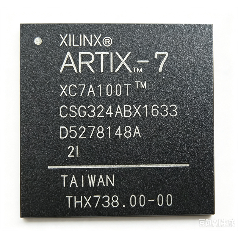
XC7A100T-1CSG324C - Artix-7 FPGA, 101K Logic Cells | AMD Xilinx
The AMD Xilinx XC7A100T-1CSG324C is a high-performance Artix-7 family FPGA delivering 101,440 logic cells, 240 DSP slices, and 4,860 Kb of block RAM in a 324-ball CSG (Chip Scale BGA) package. It operates with a core voltage of 1.0V and supports I/O standards up to 3.3V, making it suitable for cost-sensitive, high-volume applications requiring programmable logic. Data verified as of 2026-08-04. An FPGA (Field-Programmable Gate Array) is an integrated circuit that can be configured by the designer after manufacturing, allowing for custom digital logic implementations. FPGAs sit within the broader category of programmable logic devices (PLDs), which are part of the semiconductor industry. They offer a balance between the flexibility of software and the performance of fixed-function ASICs, enabling rapid prototyping and hardware acceleration. Key features include 285,000 system logic cells (equivalent), 240 DSP48E1 slices for digital signal processing, and 4,860 Kb of fast block RAM. The device supports a wide range of I/O standards including LVCMOS, LVDS, and HSTL, with up to 210 user I/O pins in the CSG324 package. The -1 speed grade provides a balance of performance and power, with a maximum clock frequency of approximately 400 MHz for internal logic. The Artix-7 architecture is built on a 28nm high-k metal gate (HKMG) process, offering low static power consumption and high logic density. The device includes integrated PCIe Gen2 blocks, XADC for analog-to-digital conversion, and GTP transceivers (up to 6.6 Gbps) for high-speed serial communication. These features make it a versatile choice for a wide range of applications. Typical applications include software-defined radio, motor control, industrial networking, and video processing. The XC7A100T-1CSG324C is particularly well-suited for applications requiring high I/O count and moderate logic resources, such as interface bridging and protocol conversion. When designing with this FPGA, careful attention must be paid to power supply decoupling and thermal management. The device requires multiple supply rails (VCCINT, VCCAUX, VCCO) and a proper power-up sequence. Use the Xilinx Power Estimator (XPE) to calculate power consumption and design an appropriate thermal solution. This page synthesizes distributor pricing, drop-in alternatives, and practical design notes not found in the AMD Xilinx datasheet, providing a comprehensive resource for engineers evaluating the XC7A100T-1CSG324C.
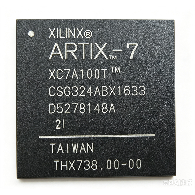
XC7A100T-1CSG324I - Artix-7 FPGA, 101K Logic Cells | AMD Xilinx
The AMD Xilinx XC7A100T-1CSG324I is a high-performance Artix-7 family FPGA delivering 101,440 logic cells, 240 DSP48E1 slices, and 4,860 Kb of block RAM in a 324-ball CSBGA package. It operates with a core voltage of 1.0V and supports I/O standards up to 3.3V, making it suitable for cost-sensitive, high-volume applications requiring low power and high throughput. Data verified as of 2026-08-04. An FPGA (Field-Programmable Gate Array) is a semiconductor device containing configurable logic blocks and programmable interconnects that can be programmed after manufacturing to implement any digital logic function. FPGAs sit within the hierarchy of programmable logic devices (PLDs), which are a subset of integrated circuits used for custom digital design without the cost and lead time of ASICs. The Artix-7 family is optimized for low power and cost, balancing performance with affordability for applications like software-defined radio, industrial motor control, and medical imaging. Key features include 285,000 system logic cells equivalent, 240 DSP slices for high-speed signal processing, 4,860 Kb of block RAM, and 6.6 Gb/s GTP transceivers. The device supports DDR3 memory interfaces up to 800 Mb/s and features a 12-bit, 1 MSPS XADC for analog monitoring. The CSG324 package offers 210 user I/O pins, providing flexibility for various board designs. The XC7A100T-1CSG324I is built on 28nm high-k metal gate (HKMG) process technology, balancing performance and power efficiency. It includes hardened memory controllers, PCIe Gen2 blocks, and a security engine for bitstream encryption. The device supports partial reconfiguration, enabling dynamic updates to logic functions without full reconfiguration. Typical applications include software-defined radio (SDR) for its DSP capabilities, industrial motor control for its real-time processing, and medical imaging for its parallel processing throughput. The low power consumption and cost-effectiveness make it ideal for high-volume products. When designing with this FPGA, ensure adequate decoupling capacitors on all power rails and follow the recommended power-up sequence to avoid latch-up. The configuration interface supports multiple modes, including JTAG, SPI, and BPI, allowing flexible system integration. This page synthesizes distributor pricing, drop-in alternatives, and practical design notes not found in the AMD Xilinx datasheet, providing engineers with a comprehensive resource for selection and implementation.