EP2S15F484C5 vs EP2S15F484C4 Comparison
Detailed side-by-side comparison of EP2S15F484C5 by Intel and EP2S15F484C4 by Intel. Compare key specifications, electrical parameters, packaging, lifecycle status, pricing, and availability to determine the best component for your design requirements.

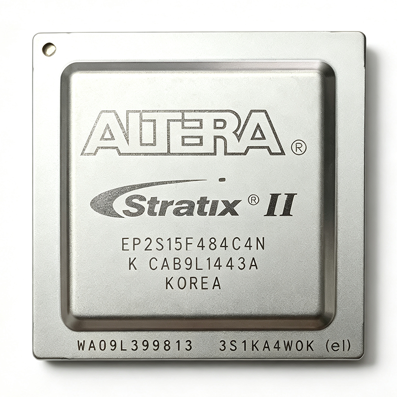
Specification Comparison
| Parameter | EP2S15F484C5 | EP2S15F484C4 |
|---|---|---|
| Brand | Intel | Intel |
| Category | FPGA & CPLD | FPGA & CPLD |
| Lifecycle Status | Obsolete | Last_time_buy |
| Stock Status | In Stock | In Stock |
| Unit Price (USD) | $185.00 | $205.00 |
| Family | Stratix II | Stratix II |
| Logic Elements (LE) | 15,600 | — |
| Adaptive Logic Modules (ALMs) | 6240 | — |
| LABs / CLBs | 780 | — |
| Embedded Memory | 409 Kbit (TriMatrix) | — |
| User I/O Count | 342 | — |
| Number of Logic Cells | 15600 | — |
| Supply Voltage (Core) | 1.2 V | [DATA_NEEDED: VCCINT nominal] |
| Maximum Operating Frequency | 609.76 MHz | — |
| Package | 484-ball FBGA (FC-FBGA) | 484-FBGA (FBGA-484) |
| Mounting Type | Surface Mount | — |
| Process Node | 90 nm | — |
| Operating Temperature Grade | Commercial (per DigiKey listing) | — |
| RoHS Status | Non-Compliant (Contains Lead) | Compliant (lead-free FBGA package) |
| Configuration Method | SRAM-based (volatile, external config device) | Serial/parallel, JTAG |
| Logic Elements (LEs) | — | 15,600 |
| Adaptive Logic Modules (ALMs) / CLBs | — | 6,240 |
| Embedded Memory (Bits) | — | 419,328 |
| Maximum User I/O | — | 342 |
| DSP Blocks | — | Yes (integrated multiplier-accumulators) |
| Package Dimensions | — | 23 mm x 23 mm |
| Ball Pitch | — | 1.0 mm |
| Process Technology | — | 90 nm CMOS |
| Core Performance | — | Up to 717 MHz |
| Speed Grade | — | C4 (-4, mid-tier) |
| Temperature Grade | — | Commercial (C): 0 C to +85 C junction |
| I/O Standards Supported | — | LVDS, LVTTL, LVCMOS, SSTL, HSTL |
| External Memory Interface | — | DDR, DDR2, QDR SRAM |