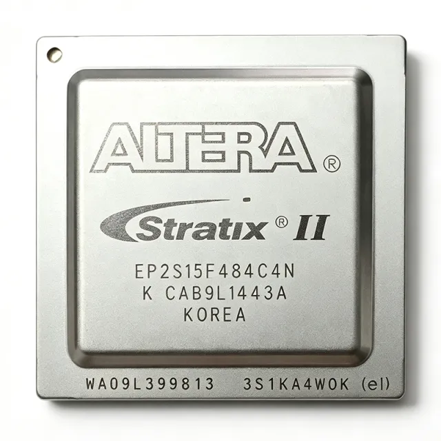
EP2S15F484C4 - Stratix II FPGA, 15.6K LEs, 484-FBGA | Intel
MPN: EP2S15F484C4 ⚠ Last Time Buy| Qty | Unit Price | Extended |
|---|---|---|
| 1 | $334.48 | $334.48 |
| 10 | $318 | $3,180.00 |
| 100 | $285 | $28,500.00 |
| 500 | $245 | $122,500.00 |
| 1,000 | $205 | $205,000.00 |
EP2S15F484C4 Overview
What is an FPGA? A Field-Programmable Gate Array (FPGA) is a reconfigurable semiconductor device that uses programmable logic blocks and interconnect fabric to implement custom digital circuits. Within the broader hierarchy, an FPGA is a type of programmable logic device (PLD), a sibling category to ASICs, microcontrollers, and DSPs. The Stratix II family sits in the upper-mid tier of Intel's (formerly Altera) FPGA portfolio, optimized for high logic density, embedded memory, and DSP performance — bridging between the lower-cost Cyclone series and the high-end Stratix V/10 families.
The EP2S15F484C4 is built on a 90 nm CMOS process and integrates DSP blocks for high-speed multiply-accumulate operations, embedded TriMatrix memory supporting true dual-port RAM, FIFO, and shift-register modes, plus high-speed transceiver support in select package variants. Its adaptive logic module architecture provides fine-grained logic packing efficiency, delivering approximately 4x the logic capacity per area compared to the prior Stratix generation. The device supports multiple I/O standards including LVDS, LVTTL, LVCMOS, SSTL, and HSTL, plus external memory interfaces to DDR, DDR2, and QDR SRAM.
Typical applications include telecommunications line cards, baseband processing, military/aerospace signal processing, industrial imaging and machine vision, and high-throughput data-acquisition systems. The 484-FBGA package provides adequate I/O count for parallel external memory buses and multi-gigabit SERDES interfaces.
Designers should use the Quartus II design suite (version supporting Stratix II) for synthesis, place-and-route, and timing closure. Pay attention to thermal dissipation at high toggle rates — the FBGA-484 package benefits from a thermal pad and forced-air cooling. The EP2S15F484C4 variant denotes the -4 speed grade (mid-tier) and C-grade temperature range (commercial, 0 C to +85 C junction). Pricing as of 2026-09-09 is approximately $334 per unit per the Heisener distributor listing.
This page synthesizes distributor inventory, drop-in alternatives, pin-by-pin package matching, and practical design notes not consolidated on any single manufacturer or distributor page.
Drop-in alternatives for EP2S15F484C4 — same package, pin-to-pin compatible. Different-package parts requiring PCB rework are excluded.
Variants in this series
Same-series models that are drop-in compatible with EP2S15F484C4 (same form factor and footprint) — differing in Package, Speed Grade, Configuration Method, Family, Adaptive Logic Modules (ALMs).
Quick Comparison Tool — Select alternative parts for side-by-side comparison:
EP2S15F484C4N
✓ In Stock
$185 / Unit
View Datasheet →EP2S15F484C3
✓ In Stock
$118 / Unit
View Datasheet →EP2S15F484C3N
✓ In Stock
$155 / Unit
View Datasheet →EP2S15F484C5
✓ In Stock
$185 / Unit
View Datasheet →EP2S30F484C4
✓ In Stock
$124 / Unit
View Datasheet →EP2S30F484C5N
✓ In Stock
$367.48 / Unit
View Datasheet →EP2C20F484C8N
✓ In Stock
$23.95 / Unit
View Datasheet →EP2S15F484C4 Maximum Ratings & Electrical Characteristics
| Family | Stratix II |
| Logic Elements (LEs) | 15,600 |
| Adaptive Logic Modules (ALMs) / CLBs | 6,240 |
| Embedded Memory (Bits) | 419,328 |
| Maximum User I/O | 342 |
| DSP Blocks | Yes (integrated multiplier-accumulators) |
| Package | 484-FBGA (FBGA-484) |
| Package Dimensions | 23 mm x 23 mm |
| Ball Pitch | 1.0 mm |
| Process Technology | 90 nm CMOS |
| Core Performance | Up to 717 MHz |
| Speed Grade | C4 (-4, mid-tier) |
| Temperature Grade | Commercial (C): 0 C to +85 C junction |
| I/O Standards Supported | LVDS, LVTTL, LVCMOS, SSTL, HSTL |
| External Memory Interface | DDR, DDR2, QDR SRAM |
| Configuration Method | Serial/parallel, JTAG |
| RoHS Status | Compliant (lead-free FBGA package) |
EP2S15F484C4 23 mm x 23 mm Pin Configuration Guide
Pin configuration for EP2S15F484C4 (23 mm x 23 mm package). This digital IC includes GPIO, communication interfaces (UART, SPI, I2C), and power pins. Refer to the manufacturer datasheet for alternate pin functions and configuration options. Essential for embedded system design and PCB layout.

No detailed pinout data available for EP2S15F484C4.
Refer to the datasheet for full pin configuration.
Typical Applications
EP2S15F484C4 is suitable for 7 applications: Telecommunications Line Cards, Baseband Signal Processing, Military and Aerospace Signal Processing, Industrial Imaging and Machine Vision, High-Throughput Data Acquisition, Medical Imaging Systems, Industrial Control and Automation.
Telecommunications Line Cards
The EP2S15F484C4 fits telecom line-card applications due to its 342 user I/O pins and integrated DSP blocks. With 6,240 ALMs and 419 Kb of TriMatrix memory, the device can implement multi-channel framer/mapper logic alongside packet-classification engines without external SRAM. Its 484-FBGA package at 23 mm x 23 mm leaves adequate board area for high-speed SERDES interfaces to SFP/SFP+ cages. Designers typically place the FPGA between a network processor and PHY transceivers, using DDR2 external memory for cell/packet buffering at line rates up to 3.125 Gbps per channel.
Recommended
Baseband Signal Processing
The EP2S15F484C4's integrated DSP blocks (each containing an 18x18 multiplier, accumulator, and adder chain) make it well-suited for wireless baseband processing such as channelization, equalization, and FFT/IFFT computation. Running at up to 717 MHz core, the device delivers sustained GMACs of DSP throughput for 3G/4G base stations. The TriMatrix memory's true dual-port mode supports simultaneous read/write of coefficients and samples, enabling pipelined baseband architectures. The 484-FBGA package handles the I/O bandwidth needed for parallel digital IF interfaces.
Recommended
Military and Aerospace Signal Processing
Defense applications such as radar signal processing, electronic warfare, and secure communications rely on the EP2S15F484C4's high logic density and DSP performance. The 484-FBGA package's 1 mm ball pitch is well-suited to MIL-STD-810 shock and vibration profiles when paired with proper underfill. Designers use the 419 Kb embedded memory for circular buffer storage of radar returns and the DSP blocks for pulse-compression filtering. For radiation-hardened applications, the commercial-temperature C4 variant is typically derated; aerospace customers commonly use the I4 industrial grade.
Recommended
Industrial Imaging and Machine Vision
Machine vision systems benefit from the EP2S15F484C4's parallel I/O bandwidth (342 pins) for multi-channel Camera Link or CoaXPress frame-grabber interfaces. The 419 Kb embedded memory serves as line-buffer storage for image preprocessing, while DSP blocks accelerate filter kernels (Sobel, Gaussian, Laplacian). At 90 nm CMOS, the device operates at the core clock rates needed for real-time processing of 10-25 megapixel camera streams. The commercial C-grade temperature range (0 to +85 C junction) is well-matched to factory-floor enclosure environments.
Recommended
High-Throughput Data Acquisition
Scientific and test-and-measurement data-acquisition systems use the EP2S15F484C4 to aggregate multiple ADC channels at sample rates above 100 MSPS. The TriMatrix memory's dual-port mode simultaneously writes ADC samples and reads them for DSP processing, eliminating external memory in many configurations. With 6,240 ALMs, the device can implement FIR filtering, digital down-conversion, and trigger logic in parallel. The 484-FBGA's thermal performance supports sustained operation at full DSP utilization when paired with moderate airflow.
Recommended
Medical Imaging Systems
Ultrasound beamformers and MRI reconstruction engines leverage the EP2S15F484C4's combination of DSP throughput and embedded memory. Per-channel FIR filtering for 64-128 element ultrasound probes can be implemented entirely on-chip using the integrated DSP blocks. The 419 Kb TriMatrix memory stores beamformed data for envelope detection, while ALMs implement apodization weight tables. Designers in medical imaging value the deterministic latency of FPGA fabric for real-time imaging pipelines, where the EP2S15F484C4's 484-FBGA package offers sufficient I/O for parallel ADC interface lanes.
Recommended
Industrial Control and Automation
The EP2S15F484C4 supports industrial protocols such as EtherCAT, PROFINET, and SERCOS III by implementing multiple real-time Ethernet channels in parallel logic. With 342 user I/O, the device can drive multi-axis motor controllers while handling encoder feedback and safety-rated I/O. The 90 nm CMOS process and commercial temperature grade suit factory-floor ambient conditions (0 to +85 C). Industrial designers commonly pair the EP2S15F484C4 with external DDR2 memory for deterministic buffering and use the embedded DSP blocks for control-loop computation.
Recommended
Recommended Products Summary
Engineering reference data for EP2S15F484C4 — comparison, design guidance, and compliance information.
Selection Guide
Comparison with Alternatives
| Parameter | This Product | EP2S15F484C4N | EP2S15F484C3 | EP2S15F484C3N | EP2S15F484C5 | EP2S30F484C4 | EP2S30F484C5N | EP2C20F484C8N |
|---|---|---|---|---|---|---|---|---|
| Brand | Intel (Altera) | Intel (Altera) | Intel (Altera) | Intel (Altera) | Intel (Altera) | Intel (Altera) | Intel (Altera) | Intel (Altera) |
| Package | 484-FBGA (23x23 mm) | 484-FBGA (23x23 mm) - same | 484-FBGA (23x23 mm) - same | 484-FBGA (23x23 mm) - same | 484-FBGA (23x23 mm) - same | 484-FBGA (23x23 mm) - same | 484-FBGA (23x23 mm) - same | 484-FBGA (23x23 mm) - same |
| Family | Stratix II | Stratix II | Stratix II | Stratix II | Stratix II | Stratix II | Stratix II | Cyclone II |
| Logic Elements | 15,600 | 15,600 (same) | 15,600 (same) | 15,600 (same) | 15,600 (same) | 33,880 (+117%) | 33,880 (+117%) | 18,752 (+20%) |
| Embedded Memory (bits) | 419,328 | 419,328 (same) | 419,328 (same) | 419,328 (same) | 419,328 (same) | 1,369,728 (+227%) | 1,369,728 (+227%) | 239,616 (-43%) |
| DSP Blocks | Yes (integrated multipliers) | Yes (same) | Yes (same) | Yes (same) | Yes (same) | Yes (more blocks) | Yes (more blocks) | No (DSP not available in Cyclone II) |
| User I/O (max) | 342 | 342 (same) | 342 (same) | 342 (same) | 342 (same) | 342 (same) | 342 (same) | 315 (-8%) |
| Speed Grade | -4 (C4 mid-tier) | -4 (same) | -3 (faster) | -3 (faster) | -5 (slower) | -4 (same speed grade, higher density) | -5 (slower) | -8 (Cyclone II grading, slower) |
Key Differentiators
- Drop-in upgrade path to 33,880 LEs without PCB rework (vs EP2S30F484C4)
- Integrated DSP blocks absent from Cyclone II alternatives (vs EP2C20F484C8N)
- Triple the embedded memory versus Cyclone II at similar pin count (vs EP2C20F484C8N)
Design Notes
The EP2S15F484C4 in the 484-FBGA package dissipates significant heat at high toggle rates, especially when DSP blocks and TriMatrix memory are heavily utilized. Estimated at 90 nm CMOS, full-utilization power can reach 5-8 W; the package's thermal pad must be soldered to a board-side thermal via array (6x6 to 8x8 vias on 1.0-1.2 mm pitch) connected to an inner copper plane. Without thermal vias, junction temperature can exceed the 85 C commercial limit even at moderate ambient.
Route all power pins (VCCINT, VCCIO, VCCA, VCCD_PLL) with wide traces or copper pours; place decoupling capacitors (100 nF and 10 uF in parallel) as close as physically possible to each power pin. The 1 mm ball pitch of the FBGA-484 demands 4-layer or 6-layer PCB stackup with controlled-impedance routing for high-speed LVDS and DDR2 interfaces. Microstrip or stripline impedance should be tuned to 50 ohm single-ended / 100 ohm differential per Quartus II board guidelines.
Use Intel's (Altera's) Stratix II pin-out file (.pin) generated by the Pin Planner in Quartus II — do not hand-map pin assignments from generic datasheets. Pin assignments for DDR2 interfaces must satisfy length-matching constraints (typically ±25 mil for data, ±50 mil for address/command). Leave all configuration pins (nCONFIG, MSEL[3:0], DATA[7:0]) accessible to a JTAG header for in-system programming and debug via SignalTap II logic analyzer.
Common pitfalls include: (1) forgetting to enable pull-ups on unused user I/O — without them, floating inputs cause excessive current draw; (2) underestimating hold-time requirements on source-synchronous interfaces at the -4 speed grade — use TimeQuest timing analyzer to verify; (3) using the I4 industrial-grade part as a drop-in for the C4 commercial part when the application is purely commercial — wasted cost; (4) ordering C3 as a drop-in for C4 when design needs C4 timing margin — C3 will fail timing closure.
For DDR2 interfaces at 267 MHz (533 MT/s), maintain differential pair length matching within 20 mil for DQS/DQ lanes. Use IBIS simulation (available through Quartus II board-level simulation) to verify signal integrity on critical nets before PCB fabrication. Series-termination resistors are typically NOT needed for Stratix II on-die termination (OCT) when configured in OCT modes, but external resistors may be required if OCT is disabled for power-saving modes.
Compliance Information
RoHS and REACH compliant per Intel/Altera Stratix II product declaration. Lead-free FBGA-484 package. Not AEC-Q100 qualified (industrial/automotive applications should consider I4 temperature grade or AEC-qualified parts). Halogen-free status not explicitly documented in verified data.







