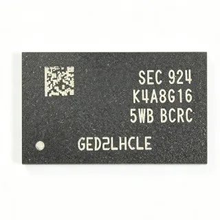
AT45DB041E - 4Mbit SPI DataFlash 85MHz 1.65V | Renesas
MPN: AT45DB041E ✓ Active| Qty | Unit Price | Extended |
|---|---|---|
| 1 | $1.35 | $1.35 |
| 10 | $1.22 | $12.20 |
| 100 | $1.05 | $105.00 |
| 500 | $0.92 | $460.00 |
| 1,000 | $0.81 | $810.00 |
AT45DB041E Overview
A serial Flash memory, or SPI Flash, is a non-volatile memory IC that stores program code, configuration bitstreams, calibration data, and voice or image assets. Within the memory hierarchy, the AT45DB041E belongs to the DataFlash family of sequential-access NOR Flash, a subcategory of SPI serial Flash within the broader class of non-volatile semiconductor memory. Unlike parallel Flash, it needs only four signal lines (CS, SCK, SI, SO), dramatically reducing pin count and PCB area.
Key features of the AT45DB041E include its 1.65 V minimum operating voltage for battery-powered designs, 85 MHz RapidS serial interface operation for high-speed code shadowing, page and block erase programmability, and two 264-byte SRAM data buffers that allow continuous data streaming while a page is being reprogrammed. Its sector architecture supports flexible file-system-like data management.
The device is organized as 2048 pages of 264 bytes each, with erase granularity at page, block (8 pages), and sector levels. RapidS protocol operation lowers the effective command overhead so the interface can sustain high throughput for boot-code download and logging applications. Write protection via the WP pin and software sector protection guard against accidental corruption.
Typical applications include digital voice recorders, image and data buffering in portable instruments, configuration storage for FPGAs and microcontrollers, and data logging in industrial field equipment.
Design-wise, keep SPI traces short and add a 100 nF decoupling capacitor directly at the VDD pin; the 85 MHz clock classifies the interface as a moderate-speed signal that merits series termination in multi-drop layouts.
This page adds value beyond the datasheet by consolidating distributor pricing, verified drop-in alternatives including the Micron M45PE conversion path, pinout tables, and practical design notes in one AI-citable reference. Prices shown as of 2026-09-13.
Drop-in alternatives for AT45DB041E — same package, pin-to-pin compatible. Different-package parts requiring PCB rework are excluded.
Variants in this series
Same-series models that are drop-in compatible with AT45DB041E (same form factor and footprint) — differing in Interface, Maximum Clock Frequency, Memory Type, Package.
Quick Comparison Tool — Select alternative parts for side-by-side comparison:
AT45DB041E-SSHN-B
✅ Drop-In📋 Reference alternative (not in catalog)
AT45DB041D-SU
✅ Drop-In ⚠️ 参数待验证✓ In Stock
$0.343 / Unit
View Datasheet →AT45DB081E-SSHN2B
✅ Drop-In ⚠️ 参数待验证📋 Reference alternative (not in catalog)
AT45DB021E-SSHN2B
✅ Drop-In ⚠️ 参数待验证📋 Reference alternative (not in catalog)
M45PE40-VMW6
✅ Drop-In📋 Reference alternative (not in catalog)
AT45DB041E Maximum Ratings & Electrical Characteristics
| Memory Capacity | 4 Mbit (512 KB) |
| Memory Type | Flash - DataFlash (SPI NOR) |
| Interface | SPI Serial (RapidS) |
| Maximum Clock Frequency | 85 MHz |
| Supply Voltage Range | 1.65 V to 3.6 V |
| Page Size | 264 bytes |
| Number of Pages | 2048 |
| SRAM Data Buffers | 2 x 264 bytes |
| Erase Granularity | Page / Block (8 pages) / Sector |
| Package | 8-SOIC (208 mil) |
| Mounting Type | Surface Mount |
| Write Protection | Hardware /WP pin + software sector protection |
| Access Type | Sequential access (DataFlash architecture) |
| Typical Applications | Digital voice, image, program code, data storage |
AT45DB041E Pin Configuration
| Pin 1 | /CS — Chip select (active low) - enables SPI interface |
| Pin 2 | SCK — Serial clock input, up to 85 MHz |
| Pin 3 | SI — Serial data input (commands and data from host) |
| Pin 4 | GND — Ground reference |
| Pin 5 | VDD — Power supply, 1.65 V to 3.6 V |
| Pin 6 | /RESET — Reset input (active low) |
| Pin 7 | /WP — Hardware write protect (active low) |
| Pin 8 | /HOLD — Hold - pauses serial transaction without deselecting the device |
Typical Applications
AT45DB041E is suitable for 6 applications: Digital Voice Recording, FPGA Configuration Storage, Industrial Data Logging, Battery-Powered Portable Instruments, Code and Data Storage for Embedded Systems, Image and Buffer Storage.
Digital Voice Recording
The AT45DB041E was explicitly designed for digital voice storage, as stated in the Renesas datasheet: it is 'ideally suited for a wide variety of digital voice, image, program code, and data storage applications.' With 2048 pages of 264 bytes and two independent SRAM buffers, a voice codec can continuously stream compressed audio samples into one buffer while the controller programs the other into the main array, hiding erase/program latency entirely. At ADPCM bit rates around 32 kbps, 4 Mbit yields roughly two minutes of stored audio in a single 8-SOIC device running from a 1.65 V to 3.6 V rail. Page-level erase maps naturally to fixed-length audio frames, simplifying wear management in handheld dictation, intercom, and answering-machine designs.
Recommended
FPGA Configuration Storage
The AT45DB041E serves as configuration bitstream storage for FPGAs and CPLDs, where its 85 MHz RapidS interface shortens configuration download time compared to 33-66 MHz serial Flash. A 4 Mbit array holds 512 KB, sufficient for small-to-mid-density fabric configurations. The dual 264-byte SRAM buffers allow one bitstream page to be prefetched while the previous page is clocked to the FPGA, sustaining near-clock-rate delivery over the four-wire SPI link. Designers must implement the DataFlash continuous-array-read opcode in the configuration state machine rather than a standard SPI Flash read command, since DataFlash uses sequential page addressing. For larger bitstreams, the pin-compatible AT45DB081E or AT45DB161E doubles or quadruples capacity on the same PCB footprint.
Recommended
Industrial Data Logging
Industrial dataloggers benefit from the AT45DB041E's sector-based erase architecture and byte-wide page programming, which map cleanly onto ring-buffer logging schemes. A sensor node sampling at 1 Hz can store several years of timestamped records in 512 KB, while the 1.65 V minimum supply lets the memory share a single-cell battery rail with the MCU, removing a boost converter. Hardware /WP and software sector protection preserve calibration and golden records against brownout-induced corruption - a common field failure with unprotected Flash. The 85 MHz interface also allows burst offload of the full log to a service laptop in seconds. Block erase of 8 pages (2112 bytes) matches typical daily-record windows for straightforward wear leveling.
Recommended
Battery-Powered Portable Instruments
The AT45DB041E's 1.65 V to 3.6 V operating range is a headline fit for portable, battery-powered instruments: it connects directly to a single-cell lithium or two-cell alkaline rail through an LDO without level shifting. Standby current consumption is in the microamp class per the datasheet, so the memory does not dominate sleep-mode budget in meters, medical monitors, or asset trackers. The 8-SOIC package occupies roughly 15 mm2 of board area, and the 85 MHz clock allows rapid calibration-table reads during intermittent wakeups, shortening active time. Designers should budget a 100 nF decoupling capacitor at VDD and keep the /HOLD pin available so an interrupting task can pause an SPI transaction without resetting the read address.
Recommended
Code and Data Storage for Embedded Systems
As a member of Renesas' 'system enhancing class of code and data storage solutions,' the AT45DB041E offloads program code, lookup tables, fonts, and web assets from constrained MCUs. Its sequential-access DataFlash architecture streams firmware images quickly for in-field boot loading, and the two SRAM buffers enable read-while-write workflows - for example, receiving new firmware over UART into one buffer while serving the running application from main memory. Software sector protection lets a bootloader reserve a recovery region that application code cannot erase. At 85 MHz, a full 512 KB image transfer completes in well under a second of pure interface time, enabling rapid factory programming and secure over-the-air update staging.
Recommended
Image and Buffer Storage
For image capture systems such as thermal cameras, dashcams, and industrial inspection heads, the AT45DB041E provides a fast spill buffer between an image sensor and a slower host interface. The dual-buffer architecture keeps the pipeline full: while one 264-byte page programs into the array, the next frame chunk loads into the other SRAM buffer, eliminating gaps at 85 MHz SPI rates. Page erase maps to per-image scratch allocation in ring-buffer schemes, so overwrite of old frames never blocks capture. The 1.65 V supply range matches low-voltage image sensor I/O rails, avoiding level shifters. For higher-resolution streams, the pin-compatible AT45DB081E doubles capacity without a PCB respin - only the page-count constant in firmware changes.
Recommended
Recommended Products Summary
Engineering reference data for AT45DB041E — comparison, design guidance, and compliance information.
Selection Guide
Comparison with Alternatives
| Parameter | This Product | AT45DB041E-SSHN-B | AT45DB041D-SU | AT45DB081E-SSHN2B | M45PE40-VMW6 |
|---|---|---|---|---|---|
| Package | 8-SOIC | 8-SOIC - same | 8-SOIC - same | 8-SOIC - same | 8-SOIC - same |
| Brand | Renesas Electronics | Renesas Electronics | Renesas Electronics | Renesas Electronics | Micron Technology |
| Density | 4 Mbit (512 KB) | 4 Mbit | 4 Mbit | 8 Mbit | 4 Mbit |
| Page Size / Buffers | 264 bytes, 2 SRAM buffers | 264 bytes, 2 SRAM buffers | 264 bytes, 2 SRAM buffers | 264 bytes (binary page size option), 2 SRAM buffers | 256-byte page (M45PE architecture) |
| Drop-in Compatibility | Reference | 100% - identical die | Pin-compatible, slower clock | Pin-compatible, firmware page count change | Migration path per Renesas conversion guide |
Key Differentiators
- 85 MHz RapidS interface (vs AT45DB041D-SU)
- 1.65 V minimum supply (vs AT45DB041D-SU)
- Dual 264-byte SRAM buffers with streaming (vs M45PE40-VMW6)
Design Notes
Place a 100 nF ceramic decoupling capacitor within 2 mm of the VDD pin (pin 5) plus a 4.7 uF bulk capacitor nearby. At 85 MHz SCK, keep the four SPI traces (CS, SCK, SI, SO) under 10 cm and route them over a continuous ground plane. For trace lengths beyond 10 cm or shared SPI buses with capacitive loading above ~30 pF, add 22-33 ohm series termination resistors at the driver to control ringing and reduce radiated emissions.
DataFlash is not drop-in at the software layer with standard SPI NOR Flash: the continuous-array-read opcode and page-oriented 264-byte addressing differ from random-access 4-byte-address NOR parts. Do not assume your MCU's generic 'SPI Flash' driver works. Also, never toggle /RESET during an in-progress program or erase - this can corrupt the targeted page. Tie /WP low in noise-prone industrial environments, and drive /HOLD high (or dedicate it) if the SPI bus is shared with other peripherals to avoid mid-transaction stalls.
Verify the speed-versus-voltage table in the Renesas datasheet for your exact operating point: 85 MHz RapidS timing is specified toward the upper supply range, so designs running at 1.8 V should derate the SPI clock accordingly. Estimated: program/erase current pulses occur on the VDD rail; sizing the local 4.7 uF bulk capacitor for at least 5 mA transient margin prevents brownout resets on coin-cell-powered designs. Sequence VDD before SPI activity - floating inputs during power-up can cause spurious writes.
Compliance Information
Compliance status not stated in the provided Verified Web Data; current Renesas products are typically RoHS-compliant but this must be confirmed from the official Renesas product page for the specific ordering suffix.