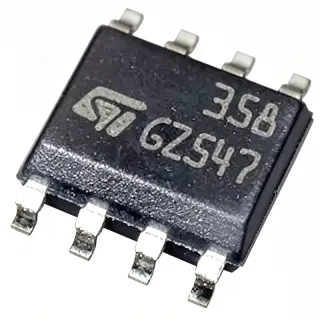
LM324QDRQ1 - Automotive Quad Op Amp 1MHz RRO | TI
MPN: LM324QDRQ1 ✓ Active| Qty | Unit Price | Extended |
|---|---|---|
| 1 | $0.55 | $0.55 |
| 10 | $0.48 | $4.80 |
| 100 | $0.39 | $39.00 |
| 500 | $0.33 | $165.00 |
| 1,000 | $0.28 | $280.00 |
Drop-in alternatives for LM324QDRQ1 — same package, pin-to-pin compatible. Different-package parts requiring PCB rework are excluded.
Quick Comparison Tool — Select alternative parts for side-by-side comparison:
LM324QDR
✅ Drop-In📋 Reference alternative (not in catalog)
LM324QT
✅ Drop-In✓ In Stock
$0.19 / Unit
View Datasheet →LM2902QDRQ1
✅ Drop-In📋 Reference alternative (not in catalog)
LM324ADR
✅ Drop-In📋 Reference alternative (not in catalog)
LM324DT
✅ Drop-In✓ In Stock
$0.0827 / Unit
View Datasheet →LM2902DT
✅ Drop-In📋 Reference alternative (not in catalog)
LM324QDRQ1 Maximum Ratings & Electrical Characteristics
| Amplifier Channels | 4 (Quad) |
| Gain Bandwidth Product | 1 MHz |
| Supply Voltage Range | 2.7 V to 5.5 V (single); +/-1.35 V to +/-2.75 V (dual) |
| Quiescent Current per Amplifier | 100 uA (typical) |
| Input Offset Voltage | 4 mV (maximum) |
| CMRR | 65 dB (typical) |
| Output Type | Rail-to-Rail Output (RRO) |
| Output Current per Channel | 160 mA per channel (per distributor listing) |
| Input Bias Current | 0.5 uA |
| Stability | Unity-gain stable (internally compensated) |
| Short-Circuit Protection | Yes |
| Qualification | AEC-Q100 (Automotive) |
| Package | 14-SOIC (D), 3.90 mm width |
| Mounting Type | Surface Mount |
| Operating Temperature | [DATA_NEEDED: operating temperature range] |
| RoHS Status | Compliant |
LM324QDRQ1 Pin Configuration
| Pin 1 | OUT1 — Amplifier 1 output |
| Pin 2 | IN1- — Amplifier 1 inverting input |
| Pin 3 | IN1+ — Amplifier 1 non-inverting input |
| Pin 4 | VCC — Positive supply |
| Pin 5 | IN2+ — Amplifier 2 non-inverting input |
| Pin 6 | IN2- — Amplifier 2 inverting input |
| Pin 7 | OUT2 — Amplifier 2 output |
| Pin 8 | OUT3 — Amplifier 3 output |
| Pin 9 | IN3- — Amplifier 3 inverting input |
| Pin 10 | IN3+ — Amplifier 3 non-inverting input |
| Pin 11 | GND / VEE — Ground or negative supply |
| Pin 12 | IN4+ — Amplifier 4 non-inverting input |
| Pin 13 | IN4- — Amplifier 4 inverting input |
| Pin 14 | OUT4 — Amplifier 4 output |
Safe Operating Area (SOA) & Thermal Characteristics
No official SOA curve available for this component. Always operate within absolute maximum ratings specified in the datasheet. Ensure adequate cooling and derate as needed.
Typical Applications
LM324QDRQ1 is suitable for 6 applications: Automotive Sensor Signal Conditioning, Battery Management System Monitoring, Motor Control Signal Chain, Low-Voltage Active Filtering, Comparators and Level Detection, Transimpedance and Buffer Front-Ends.
Automotive Sensor Signal Conditioning
The LM324QDRQ1 amplifies and filters low-level signals from temperature, pressure, and position sensors in automotive ECUs. Its AEC-Q100 qualification covers harsh under-hood environments, while the rail-to-rail output maximizes usable dynamic range on 5 V rails, and the ground-sensing common-mode input range allows direct connection of ground-referenced sensor bridges. With a 1 MHz GBW, it comfortably handles sensor bandwidths below 100 kHz with anti-alias filtering, and 100 uA per channel quiescent current keeps module-level standby current within automotive budget limits.
Recommended
Battery Management System Monitoring
In BMS front-ends, the LM324QDRQ1 buffers cell-voltage divider signals and drives ADC inputs with low output impedance. Its rail-to-rail output reaches close to the 5 V rail, preserving measurement headroom across the pack voltage range, and the 4 mV maximum offset supports cell-voltage accuracy targets when paired with calibration. The quad configuration allows simultaneous conditioning of multiple cell or thermistor channels in one package, reducing BOM count and channel-to-channel mismatch, which improves pack-level state-of-charge estimation consistency across temperature and aging.
Recommended
Motor Control Signal Chain
The LM324QDRQ1 conditions current-sense and position-feedback signals in automotive motor control systems. Placed between shunt amplifiers or Hall sensors and the MCU ADC, its 1 MHz GBW supports current-loop bandwidths of tens of kilohertz, and the rail-to-rail output uses the full ADC input span of 3.3 V controllers. Internal unity-gain stability simplifies buffer stages, while short-circuit protection adds robustness against harness faults common in 12 V automotive actuator environments. Low 400 uA total quiescent draw suits always-on auxiliary motor modules.
Recommended
Low-Voltage Active Filtering
With internal unity-gain compensation and four matched channels, the LM324QDRQ1 implements Sallen-Key and multiple-feedback active filters directly on 3.3 V or 5 V single supplies. The ground-inclusive common-mode input range allows filter networks biased at mid-supply or ground without negative rails, and the rail-to-rail output prevents signal clipping near the positive rail at large filter outputs. Channel matching within one SOIC-14 package keeps multi-stage filter corner frequencies consistent, an advantage over assembling stages from separate single op amp packages.
Recommended
Comparators and Level Detection
Open-loop or high-gain configurations of the LM324QDRQ1 serve as low-speed comparators for threshold detection, window monitors, and fault flags in 5 V automotive modules. The rail-to-rail output directly drives logic-level inputs without external level shifting, and the quad package provides four independent thresholds (overvoltage, undervoltage, overtemperature, overcurrent) in one device. For signals slower than roughly 100 kHz, the 1 MHz GBW provides adequate response, though designers needing microsecond propagation delay should select a dedicated comparator instead.
Recommended
Transimpedance and Buffer Front-Ends
The LM324QDRQ1 buffers high-impedance sources such as photodiodes and piezo sensors at modest bandwidths. With 0.5 uA input bias current, it suits applications where nanoamp-level accuracy is not critical, and the internally compensated amplifier remains stable in unity-gain buffer configurations. Placed close to the sensor with a guarded PCB trace, it drives cable capacitance to downstream ADCs. For precision photodiode work demanding sub-picoamp bias currents, engineers should instead consider JFET or CMOS input amplifiers from the same supplier portfolio.
Recommended
Recommended Products Summary
Engineering reference data for LM324QDRQ1 — comparison, design guidance, and compliance information.
Selection Guide
Comparison with Alternatives
| Parameter | This Product | LM324QDR | LM324QT | LM2902QDRQ1 | LM324DT | LM2902DT |
|---|---|---|---|---|---|---|
| Package | 14-SOIC (D) | 14-SOIC (D) - same | 14-SOIC (D) - same | 14-SOIC (D) - same | 14-SOIC - same | 14-SOIC - same |
| Brand | Texas Instruments | Texas Instruments | Texas Instruments | Texas Instruments | STMicroelectronics | STMicroelectronics |
| Automotive Qualification (AEC-Q100) | Yes | No (industrial) | Automotive family | Yes | No | Automotive family |
| Output Stage | Rail-to-Rail Output | Rail-to-Rail Output | Rail-to-Rail Output | Conventional | Conventional | Conventional |
| Channels | 4 (Quad) | 4 | 4 | 4 | 4 | 4 |
| Supply Voltage Range | 2.7 V to 5.5 V | 2.7 V to 5.5 V | [DATA_NEEDED] | 3 V to 36 V | 3 V to 32 V | 3 V to 32 V |
| Gain Bandwidth | 1 MHz | 1 MHz | 1 MHz | 1.2 MHz (typ) | 1.2 MHz (typ) | 1.2 MHz (typ) |
| Price (1 pc, as of 2026-08-29) | 0.55 USD | [DATA_NEEDED] | [DATA_NEEDED] | [DATA_NEEDED] | [DATA_NEEDED] | [DATA_NEEDED] |
Key Differentiators
- AEC-Q100 automotive qualification (vs LM324QDR)
- Rail-to-rail output maximizes low-voltage dynamic range (vs LM2902QDRQ1)
- Ground-sensing input common-mode range (vs LM324DT (ST))
Design Notes
Place a 0.1 uF ceramic decoupling capacitor within 2-3 mm of the VCC pin (pin 4) with a low-impedance via to ground. Because the LM324QDRQ1 integrates four amplifiers sharing one supply, load-transient coupling between channels appears on the shared rail; a bulk 1 uF to 4.7 uF capacitor nearby suppresses inter-channel crosstalk in multi-channel sensor boards. Keep input trace lengths short to minimize parasitic capacitance on the inverting node, which erodes phase margin.
Respect the input common-mode range of ground to VCC - 1.5 V. Signals approaching the upper rail can cause the output to saturate or behave nonlinearly, a classic LM324-family pitfall. If signals exceed this range, bias the input network at mid-supply or select a rail-to-rail input amplifier. Also verify phase-reversal behavior during fault conditions where inputs are pulled above VCC, such as load-dump events in 12 V automotive harnesses with clamped but elevated transients.
At 100 uA per amplifier, self-heating is negligible for signal-level loads, but driving low-impedance loads near the 160 mA per-channel capability raises die dissipation quickly at 5 V supplies. Estimate P = (VCC - VOUT) * IOUT per channel and verify total package power stays within SOIC-14 limits (roughly 50-100 C/W theta_JA depending on copper). For sustained high-current channel drive, add thermal relief pours under the package.
Compliance Information
AEC-Q100 qualified per internal database. RoHS compliance inferred from active TI automotive product status; REACH and halogen-free status not stated in provided data.