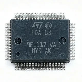
TPS7A4701RGWR - 1A, 35V Ultra-Low Noise LDO | Texas Instruments
MPN: TPS7A4701RGWR ✓ Active| Qty | Unit Price | Extended |
|---|---|---|
| 1 | $3.2467 | $3.25 |
Drop-in alternatives for TPS7A4701RGWR — same package, pin-to-pin compatible. Different-package parts requiring PCB rework are excluded.
Quick Comparison Tool — Select alternative parts for side-by-side comparison:
TPS7A4700RGWR
✅ Drop-In📋 Reference alternative (not in catalog)
TPS7A4701RGWR-Q1
✅ Drop-In📋 Reference alternative (not in catalog)
TPS7A4701RGWT
✅ Drop-In📋 Reference alternative (not in catalog)
TPS7A4701RGWR Maximum Ratings & Electrical Characteristics
| Output Type | Adjustable |
| Output Voltage Range | 1.4 V to 34 V |
| Maximum Output Current | 1 A |
| Input Voltage Range | 3 V to 35 V |
| Dropout Voltage | 200 mV at 1 A |
| Output Noise | 4.17 uVrms (20 Hz to 100 kHz) |
| PSRR | 72 dB at 1 kHz |
| Quiescent Current | 6.4 mA |
| Thermal Resistance | 31.4 C/W |
| Operating Temperature | -40C to +125C |
| Package | VQFN-20 (RGW) 5x5 mm |
| Mounting Type | Surface Mount |
| MSL Level | 2 (1 year) |
| RoHS Status | Compliant |
| Enable Pin | Yes (active-high) |
TPS7A4701RGWR Pin Configuration
| Pin 1 | OUT — Regulated output voltage |
| Pin 2 | OUT — Regulated output voltage |
| Pin 3 | OUT — Regulated output voltage |
| Pin 4 | OUT — Regulated output voltage |
| Pin 5 | GND — Ground |
| Pin 6 | EN — Enable (active high) |
| Pin 7 | IN — Input supply |
| Pin 8 | IN — Input supply |
| Pin 9 | IN — Input supply |
| Pin 10 | IN — Input supply |
| Pin 11 | NR/SS — Noise reduction/soft-start |
| Pin 12 | FB — Feedback |
| Pin 13 | GND — Ground |
| Pin 14 | GND — Ground |
| Pin 15 | GND — Ground |
| Pin 16 | GND — Ground |
| Pin 17 | GND — Ground |
| Pin 18 | GND — Ground |
| Pin 19 | GND — Ground |
| Pin 20 | GND — Ground |
Safe Operating Area (SOA) & Thermal Characteristics
No official SOA curve available for this component. Always operate within absolute maximum ratings specified in the datasheet. Ensure adequate cooling and derate as needed.
Typical Applications
TPS7A4701RGWR is suitable for 6 applications: High-End Audio DAC Power Supply, RF Transceiver Power Supply, Precision ADC Reference Buffer, Test and Measurement Instrumentation, Industrial 24V Bus Systems, Portable Medical Devices.
High-End Audio DAC Power Supply
Provides clean 5V rail for audio DACs with 4.17uVrms noise.
Recommended
RF Transceiver Power Supply
Supplies low-noise power to PLL/VCO circuits in RF transceivers.
Recommended
Precision ADC Reference Buffer
Buffers reference voltage for precision ADCs with low noise.
Recommended
Test and Measurement Instrumentation
Provides clean power rails for sensitive measurement circuits.
Recommended
Industrial 24V Bus Systems
Regulates 24V industrial bus down to low-noise rails for sensors and controllers.
Recommended
Portable Medical Devices
Provides low-noise power for battery-operated medical monitoring equipment.
Recommended
Recommended Products Summary
Engineering reference data for TPS7A4701RGWR — comparison, design guidance, and compliance information.
Selection Guide
Comparison with Alternatives
| Parameter | This Product | TPS7A4700RGWR | TPS7A4701RGWR-Q1 | TPS7A4701RGWT |
|---|---|---|---|---|
| Package | VQFN-20 (RGW) | VQFN-20 (RGW) - same | VQFN-20 (RGW) - same | VQFN-20 (RGW) - same |
| Output Current | 1 A | 1 A | 1 A | 1 A |
| Output Voltage Range | 1.4V to 34V | 1.4V to 34V | 1.4V to 34V | 1.4V to 34V |
| Enable Pin | Yes (active-high) | No | Yes (active-high) | Yes (active-high) |
| Automotive Grade | No | No | Yes (AEC-Q100) | No |
| Output Noise | 4.17 uVrms | 4.17 uVrms | 4.17 uVrms | 4.17 uVrms |
| PSRR at 1 kHz | 72 dB | 72 dB | 72 dB | 72 dB |
| Quiescent Current | 6.4 mA | 6.4 mA | 6.4 mA | 6.4 mA |
Key Differentiators
- Only VQFN-20 family member with enable pin (vs TPS7A4700RGWR)
- Automotive grade option available (vs TPS7A4701RGWR-Q1)
- Tape and reel packaging variant (vs TPS7A4701RGWT)
Design Notes
At VIN=12V, VOUT=5V, and 1A load, power dissipation is 7W. The VQFN-20 package has theta_JA of 31.4 C/W, resulting in a 220C junction temperature rise. A heatsink or at least 1 square inch of copper pour is required for reliable operation above 2W dissipation.
Place input and output capacitors as close to the IC pins as possible. Use a 10uF ceramic capacitor on the input and a 10uF ceramic capacitor on the output. Add a 0.1uF ceramic capacitor in parallel for high-frequency noise bypass.
Do not exceed the maximum input voltage of 35V. Ensure the external resistor divider uses 1% or better tolerance resistors to maintain output voltage accuracy. The NR/SS capacitor controls startup time and noise bandwidth - do not omit it.
Compliance Information
RoHS compliant per TI product page. Not AEC-Q100 qualified - choose TPS7A4701RGWR-Q1 for automotive.