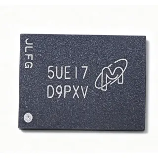
MT41K512M16VRP-107 - 8Gb DDR3L SDRAM 933MHz | Micron
MPN: MT41K512M16VRP-107 ✓ Active| Qty | Unit Price | Extended |
|---|---|---|
| 1 | $28.27 | $28.27 |
| 10 | $26.86 | $268.60 |
| 100 | $24.59 | $2,459.00 |
| 500 | $22.61 | $11,305.00 |
| 1,000 | $19.79 | $19,790.00 |
MT41K512M16VRP-107 Overview
DDR3L SDRAM (Low-Voltage Double Data Rate 3 Synchronous DRAM) is a type of volatile dynamic random-access memory that operates at 1.35V nominal, while remaining backward-compatible with 1.5V DDR3 operation. Within the memory hierarchy, SDRAM components sit at the DRAM level, providing the main system memory for processors, and DDR3L occupies the mid-generation position between DDR2 and DDR4. This TwinDie construction doubles density without requiring larger packages or finer process nodes at the module level.
Key features of the MT41K512M16VRP-107 include the wide industrial-plus operating temperature range of -40C to +95C (the IT suffix), automotive-grade screening (the :P designation), 1.35V low-voltage core operation for reduced power, and an asynchronous reset function for reliable initialization. Additional capabilities include auto self-refresh, auto precharge, data mask, dynamic on-die termination (ODT), and write leveling, which simplifies high-speed signal-integrity tuning on DDR3 controller interfaces.
The TwinDie architecture uses two 4Gb DDR3L x8 die internally; according to Micron, specifications for the base part MT41K512M8 correlate to the TwinDie manufacturing base part MT41K512M16, and the manufacturer datasheet should be read together with the 4Gb x8 data sheet for parameters not covered in the 16-page TwinDie document.
Typical applications include automotive infotainment and telematics main memory, ADAS sensor fusion platforms, industrial gateways and embedded controllers, and rugged networking equipment that requires high-density DRAM across extended temperatures. The automotive qualification makes this part particularly suited to designs where AEC-grade component selection is a system requirement.
A key design consideration: the TwinDie device presents two chip-select domains internally, so controller configuration and address mapping must match the datasheet dual-die organization, and 96-ball FBGA solder profiles must follow automotive reflow requirements.
This page synthesizes distributor pricing, drop-in alternatives, and practical design notes not found in the manufacturer datasheet, with pricing as of 2026-09-10.
Drop-in alternatives for MT41K512M16VRP-107 — same package, pin-to-pin compatible. Different-package parts requiring PCB rework are excluded.
Quick Comparison Tool — Select alternative parts for side-by-side comparison:
MT41K512M16VRP-107 AAT:P
✅ Drop-In📋 Reference alternative (not in catalog)
MT41K512M16VRN-107 IT:P
✅ Drop-In📋 Reference alternative (not in catalog)
MT41K512M16VRP-107 IT
✅ Drop-In📋 Reference alternative (not in catalog)
MT41K512M16VRP-107 Specifications
| Memory Type | DDR3L SDRAM (TwinDie) |
| Memory Size | 8 Gbit |
| Organization | 512M x 16 |
| Clock Frequency | 933 MHz (DDR3-1866) |
| Access Time | 20 ns |
| Supply Voltage | 1.35 V |
| Interface | Parallel |
| Package | 96-FBGA (8 x 14 mm) |
| Operating Temperature | -40C to +95C (IT grade) |
| Grade | Automotive (:P) |
| Architecture | TwinDie - two 4Gb DDR3L x8 die per package |
| Self Refresh | Auto self-refresh |
| Auto Precharge | Yes |
| Asynchronous Reset | Yes |
| Data Mask | Yes |
| Dynamic ODT | Yes |
| Write Leveling | Yes |
| Mounting Type | Surface Mount |
MT41K512M16VRP-107 96-fbga (8 x 14 mm) Pin Configuration Guide
Pin configuration for MT41K512M16VRP-107 (96-fbga (8 x 14 mm) package). Pin numbering, functions, and connection diagrams are defined in the manufacturer datasheet. Refer to it for the exact footprint and soldering guidelines.

No detailed pinout data available for MT41K512M16VRP-107.
Refer to the datasheet for full pin configuration.
Typical Applications
MT41K512M16VRP-107 is suitable for 6 applications: Automotive Infotainment Main Memory, ADAS Sensor Fusion Processing, Industrial Gateways and Embedded Controllers, Telematics Control Units (TCU), Rugged Networking Equipment, Test and Measurement Instrumentation.
Automotive Infotainment Main Memory
The MT41K512M16VRP-107 IT:P is purpose-built for automotive infotainment systems, where its 8Gbit TwinDie density in a single 96-ball FBGA (8 x 14 mm) package supports navigation, media playback, and HMI graphics. Its automotive-grade (:P) screening and -40C to +95C IT temperature range cover under-dash thermal environments, while 1.35V DDR3L operation reduces system power. Running at DDR3-1866 (933 MHz) with write leveling and dynamic ODT, it sustains the bandwidth needed by graphics and audio pipelines. Placed on the SoC's dedicated DDR3L bus with fly-by routing and asynchronous reset support, it provides reliable boot and runtime memory; the main trade-off is stricter PCB signal-integrity layout at 933 MHz.
Recommended
ADAS Sensor Fusion Processing
Advanced driver assistance systems aggregate camera, radar, and lidar data in SoCs that require multi-gigabit working memory. The MT41K512M16VRP-107's 8Gbit capacity in a single x16 device minimizes component count versus four smaller DDR3L chips, improving board reliability, and its automotive screening matches ADAS qualification flows. The -40C to +95C industrial-plus range and auto self-refresh preserve data across cold-start and extended-idle scenarios. At DDR3-1866, a single 16-bit channel delivers over 3.7 GB/s peak bandwidth for frame-buffer and fusion workloads. Designers should enable dynamic ODT and write leveling to meet signal integrity at 933 MHz, and verify the controller's chip-select and address mapping against the TwinDie dual-die organization documented in Micron's datasheet.
Recommended
Industrial Gateways and Embedded Controllers
Industrial IoT gateways and embedded controllers running Linux-class operating systems benefit from the MT41K512M16VRP-107's 8Gbit density and 1.35V low-voltage operation, which cuts memory subsystem power in always-on installations. The IT temperature grade (-40C to +95C) survives unconditioned factory floors and outdoor cabinets, and the 96-ball FBGA package suits compact, high-reliability boards. Auto precharge and asynchronous reset simplify power-cycling behavior in electrically noisy environments. With DDR3-1866 bandwidth, packet buffers, protocol stacks, and local logging run without memory bottlenecks. Key considerations: the automotive :P screening adds cost margin over commercial parts, so it is justified where extended temperature and long lifecycle supply are requirements rather than optional.
Recommended
Telematics Control Units (TCU)
Telematics control units require DRAM that maintains connectivity firmware, cellular protocol stacks, and logging buffers across wide temperature swings. The MT41K512M16VRP-107 IT:P fits this role with its automotive screening, -40C to +95C range, and 8Gbit TwinDie density that hosts both the connectivity stack and data logging in a single 1.35V device. Auto self-refresh preserves memory content during low-power sleep states between vehicle wake events, extending battery life. Its 96-ball FBGA footprint withstands automotive vibration profiles better than larger TSOP-type legacy packages. Designers should provision the asynchronous reset from the vehicle's power-management IC so memory re-initializes cleanly during crank and load-dump events, and size decoupling per Micron's DDR3L power recommendations.
Recommended
Rugged Networking Equipment
Industrial Ethernet switches, routers, and edge compute modules use the MT41K512M16VRP-107 as packet-buffer and control-plane memory. Its DDR3-1866 (933 MHz) interface supplies the bandwidth for line-rate forwarding tables and QoS queues, while the 512M x 16 organization matches 16-bit memory controllers in networking SoCs. The IT temperature grade supports conformally coated boards in outdoor or fanless enclosures, and 1.35V operation reduces total board power in passive-cooled designs. Because it is a TwinDie part, firmware memory maps must reflect the dual-die structure per Micron's datasheet. For replacement of legacy networking memory in the obsolete MT41K512M16VRN-107, this VRP variant is the verified drop-in substitute with identical footprint and specifications.
Recommended
Test and Measurement Instrumentation
Bench instruments, data-acquisition systems, and logic analyzers require deep capture buffers; the MT41K512M16VRP-107's 8Gbit capacity provides 1 GB of 16-bit-wide capture memory in one package, streaming at DDR3-1866 rates into controller memory. The -40C to +95C IT range accommodates instrument warm-up and environmental qualification testing, and its automotive screening provides an additional reliability margin for instruments expected to run continuous duty cycles. Dynamic ODT and write leveling simplify achieving clean signaling on 933 MHz fly-by layouts in dense PCB stacks. A design consideration: instrument designers should budget power-decoupling for the 1.35V rail under burst-write loading, and consult Micron's 4Gb x8 base-die datasheet for timing parameters not detailed in the TwinDie document.
Recommended
Recommended Products Summary
Engineering reference data for MT41K512M16VRP-107 — comparison, design guidance, and compliance information.
Selection Guide
Comparison with Alternatives
| Parameter | This Product | MT41K512M16VRP-107 AAT:P | MT41K512M16VRN-107 IT:P | MT41K512M16VRP-107 IT |
|---|---|---|---|---|
| Package | 96-FBGA (8 x 14 mm) | 96-FBGA (8 x 14 mm) - same | 96-FBGA (8 x 14 mm) - same | 96-FBGA (8 x 14 mm) - same |
| Brand | Micron Technology | Micron Technology | Micron Technology | Micron Technology |
| Memory Size | 8 Gbit | 8 Gbit | 8 Gbit | 8 Gbit |
| Organization | 512M x 16 | 512M x 16 | 512M x 16 | 512M x 16 |
| Clock Frequency | 933 MHz (DDR3-1866) | 933 MHz (DDR3-1866) | 933 MHz (DDR3-1866) | 933 MHz (DDR3-1866) |
| Supply Voltage | 1.35 V | 1.35 V | 1.35 V | 1.35 V |
| Operating Temperature | -40C to +95C (IT) | -40C to +95C (IT) | -40C to +95C (IT) | -40C to +95C (IT) |
| Lifecycle Status | Active | Active | Obsolete (per DigiKey) | Active |
Key Differentiators
- Active production with today-ship distributor availability (vs MT41K512M16VRN-107 IT:P)
- TwinDie 8Gb density in a single 96-FBGA (vs MT41K512M16VRP-107 AAT:P)
- Automotive-grade screening with IT temperature range (vs MT41K512M16VRP-107 IT)
Design Notes
At DDR3-1866 (933 MHz), route the address/command bus in a fly-by topology with on-die termination (ODT) enabled and use Micron's write leveling support to align data strobes to the clock. Keep all data-group traces length-matched within controller skew budget, and reference traces to a continuous ground plane. Because this is a TwinDie part with two internal x8 die, per-die ODT settings should be programmed per the 4Gb x8 base die recommendations referenced in the TwinDie datasheet.
The 96-ball FBGA (8 x 14 mm) requires a fanout region with via-in-pad or dog-bone escape routing for the dense ball field. Use solid power and ground planes under the package and place 1.35V decoupling (bulk plus high-frequency ceramics) close to the ball field. Follow the manufacturer's lead-free BGA reflow profile and observe MSL bake rules from the product label before mounting. Confirm footprint pad geometry against Micron's package outline drawing before releasing the PCB.
Do not treat this device as a single-die 8Gb SDRAM: it is two 4Gb x8 die, and some timing/configuration parameters live in the 4Gb x8 datasheet (MT41K512M8 correlates to base part MT41K512M16 per Micron). Also avoid sourcing the obsolete MT41K512M16VRN-107 from grey-market channel stock - use the active VRP-107 instead. Verify supply-chain authenticity for automotive-grade (:P) parts, as periodic supply tension has been reported by independent distributors.
Compliance Information
The :P suffix in Micron part numbering conventionally indicates lead-free/RoHS packaging, but explicit RoHS/REACH/AEC-Q100 status was not stated in the provided data. Confirm compliance certificates on Micron's official product page.