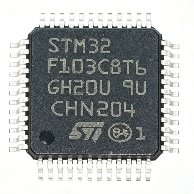
STM32F103C8T6 - 32-bit ARM Cortex-M3 MCU, 64KB Flash | STMicroelectronics
MPN: STM32F103C8T6 ✓ Active| Qty | Unit Price | Extended |
|---|---|---|
| 1 | $1.93 | $1.93 |
| 10 | $1.33 | $13.30 |
| 100 | $1.18 | $118.00 |
| 500 | $1.11 | $555.00 |
| 1,000 | $1.08 | $1,080.00 |
| 1,500 | $1.02 | $1,530.00 |
Drop-in alternatives for STM32F103C8T6 — same package, pin-to-pin compatible. Different-package parts requiring PCB rework are excluded.
Quick Comparison Tool — Select alternative parts for side-by-side comparison:
STM32F103CBT6
✓ In Stock
$1.63 / Unit
View Datasheet →GD32F103C8T6
📋 Reference alternative (not in catalog)
STM32F103R8T6
📋 Reference alternative (not in catalog)
APM32F103C8T6
📋 Reference alternative (not in catalog)
STM32F030C8T6
✓ In Stock
$0.98 / Unit
View Datasheet →STM32F103C8T6 Maximum Ratings & Electrical Characteristics
| Core | ARM Cortex-M3 |
| Max Clock Frequency | 72 MHz |
| Flash Memory | 64 KB |
| SRAM | 20 KB |
| Supply Voltage | 2.0 V to 3.6 V |
| Operating Temperature | -40C to +85C |
| Package | LQFP-48 |
| Mounting Type | Surface Mount |
| Number of I/Os | 37 |
| ADC Resolution | 12-bit |
| Number of ADC Channels | 10 |
| Timer Modules | 3 general-purpose, 1 advanced |
| Communication Interfaces | USART (2), SPI (2), I2C (2), USB 2.0 FS, CAN 2.0B |
| DMA Channels | 7 |
| Debug Interface | SWD, JTAG |
| RoHS Status | Compliant |
STM32F103C8T6 Pin Configuration
| Pin 1 | VBAT — Battery backup for RTC |
| Pin 2 | PC13 — GPIO, also used for RTC tamper |
| Pin 3 | PC14 — GPIO, also used for OSC32_IN |
| Pin 4 | PC15 — GPIO, also used for OSC32_OUT |
| Pin 5 | OSC_IN — Main oscillator input |
| Pin 6 | OSC_OUT — Main oscillator output |
| Pin 7 | NRST — Reset (active low) |
| Pin 8 | VSSA — Analog ground |
| Pin 9 | VDDA — Analog power supply |
| Pin 10 | PA0 — GPIO, ADC12_IN0, TIM2_CH1 |
| Pin 11 | PA1 — GPIO, ADC12_IN1, TIM2_CH2 |
| Pin 12 | PA2 — GPIO, ADC12_IN2, TIM2_CH3 |
| Pin 13 | PA3 — GPIO, ADC12_IN3, TIM2_CH4 |
| Pin 14 | PA4 — GPIO, SPI1_NSS, DAC_OUT1 |
| Pin 15 | PA5 — GPIO, SPI1_SCK, DAC_OUT2 |
| Pin 16 | PA6 — GPIO, SPI1_MISO, TIM3_CH1 |
| Pin 17 | PA7 — GPIO, SPI1_MOSI, TIM3_CH2 |
| Pin 18 | PB0 — GPIO, TIM3_CH3, ADC12_IN8 |
| Pin 19 | PB1 — GPIO, TIM3_CH4, ADC12_IN9 |
| Pin 20 | PB2 — GPIO, BOOT1 |
| Pin 21 | PB10 — GPIO, I2C2_SCL, USART3_TX |
| Pin 22 | PB11 — GPIO, I2C2_SDA, USART3_RX |
| Pin 23 | PB12 — GPIO, SPI2_NSS, I2C2_SMBA |
| Pin 24 | PB13 — GPIO, SPI2_SCK, USART3_CTS |
| Pin 25 | PB14 — GPIO, SPI2_MISO, USART3_RTS |
| Pin 26 | PB15 — GPIO, SPI2_MOSI, TIM1_CH3N |
| Pin 27 | PC13 — GPIO, RTC_AF1 |
| Pin 28 | PC14 — GPIO, OSC32_IN |
| Pin 29 | PC15 — GPIO, OSC32_OUT |
| Pin 30 | VSS_1 — Ground |
| Pin 31 | VDD_1 — Power supply |
| Pin 32 | VDDA — Analog power supply |
| Pin 33 | VSSA — Analog ground |
| Pin 34 | PA8 — GPIO, TIM1_CH1, MCO |
| Pin 35 | PA9 — GPIO, TIM1_CH2, USART1_TX |
| Pin 36 | PA10 — GPIO, TIM1_CH3, USART1_RX |
| Pin 37 | PA11 — GPIO, USART1_CTS, USB_DM |
| Pin 38 | PA12 — GPIO, USART1_RTS, USB_DP |
| Pin 39 | PA13 — GPIO, SWDIO |
| Pin 40 | PA14 — GPIO, SWCLK |
| Pin 41 | PA15 — GPIO, JTDI |
| Pin 42 | PB3 — GPIO, JTDO |
| Pin 43 | PB4 — GPIO, NJTRST |
| Pin 44 | PB5 — GPIO, I2C1_SMBA |
| Pin 45 | PB6 — GPIO, I2C1_SCL, TIM4_CH1 |
| Pin 46 | PB7 — GPIO, I2C1_SDA, TIM4_CH2 |
| Pin 47 | BOOT0 — Boot mode selection |
| Pin 48 | VDD_2 — Power supply |
Safe Operating Area (SOA) & Thermal Characteristics
No official SOA curve available for this digital IC. Always operate within absolute maximum ratings specified in the datasheet. Ensure adequate cooling and derate as needed.
Typical Applications
STM32F103C8T6 is suitable for 6 applications: Industrial Control, IoT Gateway, Medical Monitoring Device, Automotive Body Control, Consumer Electronics, Data Logging System.
Industrial Control
Used in PLCs, motor drives, and automation controllers.
IoT Gateway
Acts as a central hub for sensor data collection and communication.
Medical Monitoring Device
Powers portable health monitors with low-power operation.
Automotive Body Control
Manages lighting, wipers, and window controls.
Consumer Electronics
Embedded in smart home devices, drones, and toys.
Data Logging System
Records sensor data to SD card or transmits via USB.