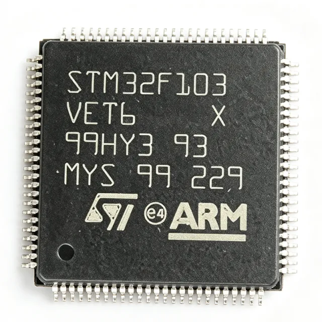
STM32F103VET6 - 512KB Flash ARM Cortex-M3 MCU | STMicroelectronics
MPN: STM32F103VET6 ✓ Active| Qty | Unit Price | Extended |
|---|---|---|
| 1 | $8.5 | $8.50 |
| 10 | $7.8 | $78.00 |
| 100 | $6.9 | $690.00 |
| 500 | $6.2 | $3,100.00 |
| 1,000 | $5.6 | $5,600.00 |
Drop-in alternatives for STM32F103VET6 — same package, pin-to-pin compatible. Different-package parts requiring PCB rework are excluded.
Quick Comparison Tool — Select alternative parts for side-by-side comparison:
STM32F103VET6TR
✅ Drop-In📋 Reference alternative (not in catalog)
STM32F103VCT6
✅ Drop-In✓ In Stock
$5.6 / Unit
View Datasheet →STM32F103VDT6
✅ Drop-In✓ In Stock
$7.1591 / Unit
View Datasheet →GD32F103VET6
✅ Drop-In📋 Reference alternative (not in catalog)
APM32F103VET6
✅ Drop-In📋 Reference alternative (not in catalog)
STM32F103VET6 Maximum Ratings & Electrical Characteristics
| Core | ARM Cortex-M3 |
| Max Clock Frequency | 72 MHz |
| Flash Memory | 512 KB |
| SRAM | 64 KB |
| Supply Voltage Range | 2.0 V to 3.6 V |
| Package | LQFP-100 |
| GPIO Pins | 80 |
| ADC | 3x 12-bit |
| DAC | 2x 12-bit |
| Timers | 8x 16-bit, 2x 32-bit |
| Communication Interfaces | USART, SPI, I2C, USB, CAN, SDIO |
| DMA | 12-channel |
| Operating Temperature Range | -40°C to +85°C |
| Process Technology | 130nm |
| Debug Interface | SWD, JTAG |
| RoHS Status | Compliant |
STM32F103VET6 Pin Configuration
| Pin 1 | VBAT — Backup battery supply for RTC and backup registers |
| Pin 2 | PC13 — GPIO or RTC output |
| Pin 3 | PC14 — GPIO or OSC32_IN |
| Pin 4 | PC15 — GPIO or OSC32_OUT |
| Pin 5 | PD0 — GPIO or OSC_IN |
| Pin 6 | PD1 — GPIO or OSC_OUT |
| Pin 7 | NRST — Reset (active low) |
| Pin 8 | VSSA — Analog ground |
| Pin 9 | VDDA — Analog power supply |
| Pin 10 | PA0 — GPIO/ADC12_IN0/TIM2_CH1 |
| Pin 11 | PA1 — GPIO/ADC12_IN1/TIM2_CH2 |
| Pin 12 | PA2 — GPIO/ADC12_IN2/TIM2_CH3/USART2_TX |
| Pin 13 | PA3 — GPIO/ADC12_IN3/TIM2_CH4/USART2_RX |
| Pin 14 | PA4 — GPIO/ADC12_IN4/SPI1_NSS/DAC_OUT1 |
| Pin 15 | PA5 — GPIO/ADC12_IN5/SPI1_SCK/DAC_OUT2 |
| Pin 16 | PA6 — GPIO/ADC12_IN6/SPI1_MISO/TIM3_CH1 |
| Pin 17 | PA7 — GPIO/ADC12_IN7/SPI1_MOSI/TIM3_CH2 |
| Pin 18 | PB0 — GPIO/ADC12_IN8/TIM3_CH3 |
| Pin 19 | PB1 — GPIO/ADC12_IN9/TIM3_CH4 |
| Pin 20 | PB2 — GPIO/BOOT1 |
| Pin 21 | PB10 — GPIO/I2C2_SCL/USART3_TX |
| Pin 22 | PB11 — GPIO/I2C2_SDA/USART3_RX |
| Pin 23 | PB12 — GPIO/SPI2_NSS/I2C2_SMBA |
| Pin 24 | PB13 — GPIO/SPI2_SCK |
| Pin 25 | PB14 — GPIO/SPI2_MISO |
| Pin 26 | PB15 — GPIO/SPI2_MOSI |
| Pin 27 | PD8 — GPIO/FSMC_D13 |
| Pin 28 | PD9 — GPIO/FSMC_D14 |
| Pin 29 | PD10 — GPIO/FSMC_D15 |
| Pin 30 | PD11 — GPIO/FSMC_A16 |
| Pin 31 | PD12 — GPIO/FSMC_A17 |
| Pin 32 | PD13 — GPIO/FSMC_A18 |
| Pin 33 | PD14 — GPIO/FSMC_A19 |
| Pin 34 | PD15 — GPIO/FSMC_A20 |
| Pin 35 | PE0 — GPIO/FSMC_NBL0 |
| Pin 36 | PE1 — GPIO/FSMC_NBL1 |
| Pin 37 | PE2 — GPIO/FSMC_A23 |
| Pin 38 | PE3 — GPIO/FSMC_A19 |
| Pin 39 | PE4 — GPIO/FSMC_A20 |
| Pin 40 | PE5 — GPIO/FSMC_A21 |
| Pin 41 | PE6 — GPIO/FSMC_A22 |
| Pin 42 | VSS — Ground |
| Pin 43 | VDD — Power supply |
| Pin 44 | PE7 — GPIO/FSMC_D4 |
| Pin 45 | PE8 — GPIO/FSMC_D5 |
| Pin 46 | PE9 — GPIO/FSMC_D6 |
| Pin 47 | PE10 — GPIO/FSMC_D7 |
| Pin 48 | PE11 — GPIO/FSMC_D8 |
| Pin 49 | PE12 — GPIO/FSMC_D9 |
| Pin 50 | PE13 — GPIO/FSMC_D10 |
| Pin 51 | PE14 — GPIO/FSMC_D11 |
| Pin 52 | PE15 — GPIO/FSMC_D12 |
| Pin 53 | PB3 — GPIO/JTDO/SPI1_SCK |
| Pin 54 | PB4 — GPIO/JNTRST/SPI1_MISO |
| Pin 55 | PB5 — GPIO/I2C1_SMBA/SPI1_MOSI |
| Pin 56 | PB6 — GPIO/I2C1_SCL/TIM4_CH1 |
| Pin 57 | PB7 — GPIO/I2C1_SDA/TIM4_CH2 |
| Pin 58 | BOOT0 — Boot mode selection |
| Pin 59 | PB8 — GPIO/CAN_RX/TIM4_CH3 |
| Pin 60 | PB9 — GPIO/CAN_TX/TIM4_CH4 |
| Pin 61 | VSS — Ground |
| Pin 62 | VDD — Power supply |
| Pin 63 | PC0 — GPIO/ADC12_IN10 |
| Pin 64 | PC1 — GPIO/ADC12_IN11 |
| Pin 65 | PC2 — GPIO/ADC12_IN12 |
| Pin 66 | PC3 — GPIO/ADC12_IN13 |
| Pin 67 | PC4 — GPIO/ADC12_IN14 |
| Pin 68 | PC5 — GPIO/ADC12_IN15 |
| Pin 69 | PC6 — GPIO/TIM8_CH1/SDIO_D6 |
| Pin 70 | PC7 — GPIO/TIM8_CH2/SDIO_D7 |
| Pin 71 | PC8 — GPIO/TIM8_CH3/SDIO_D0 |
| Pin 72 | PC9 — GPIO/TIM8_CH4/SDIO_D1 |
| Pin 73 | PA8 — GPIO/USART1_CK/TIM1_CH1 |
| Pin 74 | PA9 — GPIO/USART1_TX/TIM1_CH2 |
| Pin 75 | PA10 — GPIO/USART1_RX/TIM1_CH3 |
| Pin 76 | PA11 — GPIO/USART1_CTS/CAN_RX/USB_DM |
| Pin 77 | PA12 — GPIO/USART1_RTS/CAN_TX/USB_DP |
| Pin 78 | PA13 — GPIO/JTMS-SWDIO |
| Pin 79 | VSS — Ground |
| Pin 80 | VDD — Power supply |
| Pin 81 | PA14 — GPIO/JTCK-SWCLK |
| Pin 82 | PA15 — GPIO/JTDI/TIM2_CH1_ETR |
| Pin 83 | PC10 — GPIO/SDIO_D2/USART3_TX |
| Pin 84 | PC11 — GPIO/SDIO_D3/USART3_RX |
| Pin 85 | PC12 — GPIO/SDIO_CK/USART3_CK |
| Pin 86 | PD2 — GPIO/SDIO_CMD |
| Pin 87 | PD3 — GPIO/FSMC_CLK |
| Pin 88 | PD4 — GPIO/FSMC_NOE |
| Pin 89 | PD5 — GPIO/FSMC_NWE |
| Pin 90 | PD6 — GPIO/FSMC_NWAIT |
| Pin 91 | PD7 — GPIO/FSMC_NE1 |
| Pin 92 | VSS — Ground |
| Pin 93 | VDD — Power supply |
| Pin 94 | PE7 — GPIO/FSMC_D4 |
| Pin 95 | PE8 — GPIO/FSMC_D5 |
| Pin 96 | PE9 — GPIO/FSMC_D6 |
| Pin 97 | PE10 — GPIO/FSMC_D7 |
| Pin 98 | PE11 — GPIO/FSMC_D8 |
| Pin 99 | PE12 — GPIO/FSMC_D9 |
| Pin 100 | PE13 — GPIO/FSMC_D10 |
Safe Operating Area (SOA) & Thermal Characteristics
No official SOA curve available for this digital IC. Always operate within absolute maximum ratings specified in the datasheet. Ensure adequate cooling and derate as needed.
Typical Applications
STM32F103VET6 is suitable for 6 applications: Industrial Control Systems, Motor Drives, Medical Devices, Consumer Electronics, IoT Gateways, Automotive Electronics.
Industrial Control Systems
The STM32F103VET6 is ideal for industrial control systems due to its 72 MHz ARM Cortex-M3 core, 512 KB Flash, and rich peripheral set. It can manage multiple sensors and actuators while communicating over CAN or Ethernet. Its robust GPIO count (80 pins) allows direct interfacing with relays, motor drivers, and industrial sensors. The device's wide operating temperature range (-40°C to +85°C) ensures reliable operation in harsh factory environments. With multiple timers and ADCs, it can handle precise timing and analog signal acquisition for closed-loop control. The CAN interface enables robust communication in industrial networks, while the DMA controller offloads data transfer tasks from the CPU, improving overall system efficiency. Designers can leverage the STM32Cube ecosystem for rapid development and code reuse.
Recommended
Motor Drives
The STM32F103VET6 excels in motor drive applications due to its high-speed timers (up to 72 MHz) and multiple PWM channels. It can generate precise PWM signals for controlling brushless DC (BLDC) motors, stepper motors, and AC induction motors. The device's 12-bit ADCs enable accurate current sensing and position feedback, essential for field-oriented control (FOC). With 512 KB Flash, it can store complex motor control algorithms, including sensorless FOC and trapezoidal control. The CAN interface allows synchronization with other motor drives in multi-axis systems. The device's robust I/O structure and 5V-tolerant pins simplify interfacing with gate drivers and current sensors. Designers can use the STM32 Motor Control SDK to accelerate development, reducing time-to-market for industrial and automotive motor control applications.
Recommended
Medical Devices
The STM32F103VET6 is well-suited for medical devices such as patient monitors, infusion pumps, and diagnostic equipment. Its 72 MHz core and 512 KB Flash provide ample processing power for real-time signal processing and data logging. The device's multiple ADCs can acquire biomedical signals like ECG and SpO2 with high resolution. The low-power modes help extend battery life in portable devices. The rich communication interfaces (USB, UART, SPI, I2C) enable connectivity with sensors, displays, and wireless modules. The device's reliability and long-term availability make it a trusted choice for medical applications. Designers can implement safety-critical features using the device's built-in watchdog timers and CRC calculation unit. The wide operating temperature range ensures consistent performance in clinical environments.
Recommended
Consumer Electronics
The STM32F103VET6 is a popular choice for consumer electronics like smart home hubs, wearable devices, and gaming peripherals. Its 72 MHz ARM Cortex-M3 core delivers responsive user interfaces and efficient processing of sensor data. The 512 KB Flash allows storing firmware updates and user preferences. The device's USB interface enables direct connection to PCs and smartphones for data transfer and charging. With multiple timers and PWM channels, it can drive LEDs, buzzers, and haptic actuators. The low-power modes help conserve battery in portable devices. The device's small LQFP-100 package fits compact PCB designs. The extensive STM32 ecosystem, including HAL libraries and development boards, accelerates prototyping and production.
Recommended
IoT Gateways
The STM32F103VET6 serves as an efficient IoT gateway controller, managing communication between sensors, actuators, and cloud services. Its 72 MHz core and 512 KB Flash can handle protocol stacks like MQTT and CoAP. The device's multiple UARTs, SPI, and I2C interfaces connect to various sensors and wireless modules (Wi-Fi, LoRa, Zigbee). The Ethernet capability (via external PHY) enables wired connectivity. The device's DMA controller offloads data transfer, improving throughput. With robust security features like a unique device ID and CRC unit, it supports secure firmware updates. The low-power modes are crucial for battery-powered gateways. The device's long lifecycle and industrial temperature range make it suitable for outdoor deployments.
Recommended
Automotive Electronics
The STM32F103VET6 is used in automotive electronics such as body control modules, dashboard clusters, and telematics units. Its 72 MHz ARM Cortex-M3 core and 512 KB Flash handle complex control algorithms and data logging. The device's CAN interface is essential for in-vehicle networking. The multiple timers and PWM channels control lighting, wipers, and HVAC systems. The device's wide operating temperature range (-40°C to +85°C) meets automotive requirements. The 12-bit ADCs monitor battery voltage and sensor inputs. The device's robust I/O structure and 5V-tolerant pins interface directly with automotive relays and switches. While not AEC-Q100 qualified, it is widely used in non-safety-critical automotive applications. Designers can use the STM32CubeMX for configuration and the HAL library for rapid development.
Recommended
Recommended Products Summary
Engineering reference data for STM32F103VET6 — comparison, design guidance, and compliance information.
Selection Guide
Comparison with Alternatives
| Parameter | This Product | STM32F103VET6TR | STM32F103VCT6 | STM32F103VDT6 | GD32F103VET6 | APM32F103VET6 |
|---|---|---|---|---|---|---|
| Package | LQFP-100 | LQFP-100 | LQFP-100 | LQFP-100 | LQFP-100 | LQFP-100 |
| Brand | STMicroelectronics | STMicroelectronics | STMicroelectronics | STMicroelectronics | GigaDevice | Geehy |
| Core | ARM Cortex-M3 | ARM Cortex-M3 | ARM Cortex-M3 | ARM Cortex-M3 | ARM Cortex-M3 | ARM Cortex-M3 |
| Max Clock Frequency | 72 MHz | 72 MHz | 72 MHz | 72 MHz | 108 MHz | 96 MHz |
| Flash Memory | 512 KB | 512 KB | 256 KB | 384 KB | 512 KB | 512 KB |
| SRAM | 64 KB | 64 KB | 48 KB | 64 KB | 64 KB | 64 KB |
| GPIO Pins | 80 | 80 | 80 | 80 | 80 | 80 |
| Supply Voltage Range | 2.0V to 3.6V | 2.0V to 3.6V | 2.0V to 3.6V | 2.0V to 3.6V | 2.6V to 3.6V | 2.0V to 3.6V |
| Operating Temperature Range | -40°C to +85°C | -40°C to +85°C | -40°C to +85°C | -40°C to +85°C | -40°C to +85°C | -40°C to +85°C |
Key Differentiators
- Larger Flash and SRAM compared to STM32F103VCT6 (vs STM32F103VCT6)
- Higher maximum clock frequency than GD32F103VET6 (vs GD32F103VET6)
- Wider supply voltage range than GD32F103VET6 (vs GD32F103VET6)
Design Notes
Decouple each VDD pin with a 100nF ceramic capacitor placed as close to the pin as possible, and add a 4.7uF bulk capacitor on the main power rail. For VDDA, use a 1uF capacitor and a ferrite bead to isolate analog noise. Ensure VDD and VDDA are connected to the same supply to avoid latch-up.
Follow the layout guidelines in the STM32F103VE datasheet: keep the crystal oscillator (HSE) traces short and shielded, place the decoupling capacitors close to the power pins, and provide a solid ground plane. For the USB interface, route the D+ and D- lines as a differential pair with 90-ohm impedance.
Ensure the BOOT0 pin is properly configured to select the desired boot mode. For normal operation, connect BOOT0 to GND through a 10k resistor. Also, verify that the NRST pin has a 100nF capacitor to ground to prevent noise-induced resets. Do not leave unused GPIO pins floating; configure them as outputs or enable internal pull-ups/pull-downs.
Compliance Information
RoHS compliant per STMicroelectronics product page. Not AEC-Q100 qualified; for automotive use, consider STM32F103VET6TR or other automotive-grade variants.