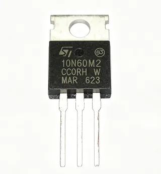
STP12N60M2 - 12A, 600V N-Channel Power MOSFET | STMicroelectronics
MPN: STP12N60M2 ✓ Active| Qty | Unit Price | Extended |
|---|---|---|
| 1 | $1.85 | $1.85 |
| 10 | $1.66 | $16.60 |
| 100 | $1.48 | $148.00 |
| 500 | $1.33 | $665.00 |
| 1,000 | $1.2 | $1,200.00 |
Drop-in alternatives for STP12N60M2 — same package, pin-to-pin compatible. Different-package parts requiring PCB rework are excluded.
Quick Comparison Tool — Select alternative parts for side-by-side comparison:
STP12N60M2-EP
✅ Drop-In📋 Reference alternative (not in catalog)
STP12N60M2FP
⚡ Same Package📋 Reference alternative (not in catalog)
IPP60R099CP
✅ Drop-In📋 Reference alternative (not in catalog)
FCP12N60
✅ Drop-In📋 Reference alternative (not in catalog)
TK12A60D
✅ Drop-In📋 Reference alternative (not in catalog)
STP12N60M2 Maximum Ratings & Electrical Characteristics
| Polarity | N-Channel |
| Drain-Source Voltage (VDS) | 600 V |
| Continuous Drain Current (ID) at 25°C | 12 A |
| On-Resistance (RDS(on)) | 0.38 Ω typical |
| Gate Charge (Qg) | 30 nC |
| Gate-Source Voltage (VGS) | ±25 V |
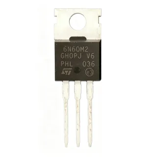
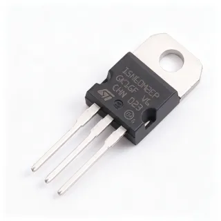
| Package | TO-220 |
| Mounting Type | Through Hole |
| Technology | MDmesh M2 |
| Avalanche Energy Rating | 100% avalanche tested |
| Thermal Resistance (Junction-to-Ambient) | 62.5 °C/W |
| Operating Temperature Range | [DATA_NEEDED: Operating Temperature Range] |
| Power Dissipation (PD) | [DATA_NEEDED: Power Dissipation] |
| RoHS Status | Compliant |
| Body Diode Recovery | Fast recovery |
STP12N60M2 Pin Configuration
| Pin 1 | Gate — Gate terminal for controlling the MOSFET |
| Pin 2 | Drain — Drain terminal, connected to the heatsink tab |
| Pin 3 | Source — Source terminal |
Safe Operating Area
Typical Applications
STP12N60M2 is suitable for 6 applications: Switch-Mode Power Supplies (SMPS), Power Factor Correction (PFC), LED Lighting Drivers, Motor Control, Solar Inverters, Battery Chargers.
Switch-Mode Power Supplies (SMPS)
The STP12N60M2 is ideal for SMPS primary-side switching due to its 600V breakdown voltage and low on-resistance. In a flyback converter, it can handle high voltage stress while minimizing conduction losses. The low gate charge (30nC) enables fast switching, reducing switching losses and improving efficiency. Designers should ensure proper gate drive (10V) and use a heatsink for high-power operation.
Recommended
Power Factor Correction (PFC)
In PFC boost converters, the STP12N60M2 handles high voltage stress (up to 600V) while maintaining low conduction losses. Its fast body diode recovery is beneficial for continuous conduction mode (CCM) operation. The low on-resistance (0.38Ω) reduces power dissipation, improving overall efficiency. Designers should consider the thermal resistance (62.5°C/W) and use adequate heatsinking.
Recommended
LED Lighting Drivers
The STP12N60M2 is suitable for LED drivers requiring high voltage and current handling. Its 600V rating allows direct connection to rectified mains (up to 400V DC). The low gate charge enables high-frequency switching, reducing the size of magnetic components. The device's avalanche ruggedness ensures reliability in transient conditions. Use a heatsink for continuous operation at high currents.
Recommended
Motor Control
In motor control applications, the STP12N60M2 can be used in the inverter stage of variable frequency drives. Its 600V rating is suitable for 230V AC motor drives. The fast switching capability reduces switching losses, and the low on-resistance minimizes conduction losses. The body diode's fast recovery is beneficial for freewheeling currents. Ensure proper gate drive and snubber circuits for inductive loads.
Recommended
Solar Inverters
The STP12N60M2 is used in solar inverter DC-DC boost stages and inverter bridges. Its high voltage rating (600V) is suitable for photovoltaic panel voltages. The low on-resistance reduces losses, improving conversion efficiency. The device's avalanche ruggedness ensures reliability under lightning-induced transients. Designers should consider thermal management for outdoor operation.
Recommended
Battery Chargers
In battery chargers, the STP12N60M2 is used in the power stage to convert AC to DC. Its 600V rating allows direct connection to mains. The low gate charge enables efficient high-frequency switching, reducing transformer size. The device's low on-resistance minimizes heat generation. Use a heatsink for continuous charging at high currents.
Recommended
Recommended Products Summary
Engineering reference data for STP12N60M2 — comparison, design guidance, and compliance information.
Selection Guide
Comparison with Alternatives
| Parameter | This Product | STP12N60M2-EP | IPP60R099CP | FCP12N60 |
|---|---|---|---|---|
| Package | TO-220 | TO-220 | TO-220 | TO-220 |
| Brand | STMicroelectronics | STMicroelectronics | Infineon | onsemi |
| Drain-Source Voltage (VDS) | 600 V | 600 V | 600 V | 600 V |
| Continuous Drain Current (ID) | 12 A | 12 A | 12 A | 12 A |
| On-Resistance (RDS(on)) | 0.38 Ω | 0.38 Ω | 0.099 Ω | 0.38 Ω |
| Gate Charge (Qg) | 30 nC | 30 nC | 45 nC | 30 nC |
| Avalanche Ruggedness | 100% tested | Enhanced | 100% tested | 100% tested |
| Operating Temperature Range | [DATA_NEEDED] | -55 to 150°C | -55 to 150°C | -55 to 150°C |
Key Differentiators
- Low gate charge (30nC) enables fast switching (vs IPP60R099CP)
- 100% avalanche tested for reliability (vs FCP12N60)
- Enhanced version available (STP12N60M2-EP) (vs IPP60R099CP)
Design Notes
The STP12N60M2 has a junction-to-ambient thermal resistance of 62.5°C/W. For high-power applications, a heatsink is essential. For example, at 12A and 0.38Ω, conduction losses are approximately 55W, which would cause a temperature rise of over 3400°C without a heatsink. Use a heatsink with a thermal resistance of less than 1°C/W for reliable operation.
For TO-220 packages, ensure the drain tab is properly soldered to a large copper area for heat dissipation. Keep the gate drive traces short and use a gate resistor (typically 10Ω) to reduce ringing. Place a 100nF ceramic capacitor close to the gate-source terminals to suppress high-frequency noise.
Do not exceed the maximum gate-source voltage of ±25V. Use a zener diode or TVS for gate protection. Also, ensure the drain-source voltage does not exceed 600V, especially during switching transients. Consider using a snubber circuit to limit voltage spikes in inductive load switching.
Compliance Information
RoHS compliance confirmed from STMicroelectronics product page. Other compliance data not available in provided data.