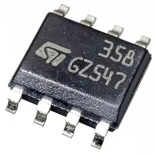
TLV2452AIDGKR-Q1 - Dual 220kHz RRIO Op Amp, 23uA | TI
MPN: TLV2452AIDGKR-Q1 ✓ Active| Qty | Unit Price | Extended |
|---|---|---|
| 1 | $1.1 | $1.10 |
| 10 | $0.99 | $9.90 |
| 100 | $0.82 | $82.00 |
| 500 | $0.68 | $340.00 |
| 1,000 | $0.55 | $550.00 |
Drop-in alternatives for TLV2452AIDGKR-Q1 — same package, pin-to-pin compatible. Different-package parts requiring PCB rework are excluded.
Quick Comparison Tool — Select alternative parts for side-by-side comparison:
TLV2452AIDGKR
✅ Drop-In✓ In Stock
$0.55 / Unit
View Datasheet →TLV2452QDGKRQ1
✅ Drop-In📋 Reference alternative (not in catalog)
TLV9152IDGKR
⚡ Same Package✓ In Stock
$0.38 / Unit
View Datasheet →MCP6442-E/MC
⚡ Same Package📋 Reference alternative (not in catalog)
TLV2452AIDGKR-Q1 Maximum Ratings & Electrical Characteristics
| Number of Channels | 2 (Dual) |
| Gain-Bandwidth Product | 220 kHz |
| Quiescent Current per Channel | 23 uA |
| Supply Voltage Range | [DATA_NEEDED: exact min/max single-supply range, see TLV245x datasheet] |
| Input/Output Type | Rail-to-Rail Input/Output (RRIO) |
| Automotive Qualification | AEC-Q100 Grade 1 |
| Operating Temperature Range | -40C to +125C |
| Package | VSSOP-8 (DGK) |
| Mounting Type | Surface Mount |
| Shutdown Feature | No (TLV2452 variant) |
| Slew Rate | [DATA_NEEDED: slew rate, see datasheet] |
| Input Offset Voltage | [DATA_NEEDED: Vos, see datasheet] |
| Marking Code | ABJ (family marking per Jotrin) |
| RoHS Status | Compliant |
| Moisture Sensitivity Level | [DATA_NEEDED: MSL, see datasheet] |
TLV2452AIDGKR-Q1 Pin Configuration
| Pin 1 | OUT A — Channel A output |
| Pin 2 | IN A- — Channel A inverting input |
| Pin 3 | IN A+ — Channel A non-inverting input |
| Pin 4 | V- — Negative supply / ground |
| Pin 5 | IN B+ — Channel B non-inverting input |
| Pin 6 | IN B- — Channel B inverting input |
| Pin 7 | OUT B — Channel B output |
| Pin 8 | V+ — Positive supply |
Safe Operating Area (SOA) & Thermal Characteristics
No official SOA curve available for this component. Always operate within absolute maximum ratings specified in the datasheet. Ensure adequate cooling and derate as needed.
Typical Applications
TLV2452AIDGKR-Q1 is suitable for 6 applications: Automotive Battery Monitoring, Low-Power Sensor Signal Conditioning, Portable and Wearable Instrumentation, Automotive 12V Rail Sensing and Supervision, MCU ADC Driver and Filtering Stage, Industrial 4-20mA Transmitter Loops.
Automotive Battery Monitoring
The TLV2452AIDGKR-Q1's 23 uA per channel quiescent current minimizes standby drain in always-on automotive battery-sense front ends, while AEC-Q100 Grade 1 qualification (-40C to +125C) guarantees operation across under-hood and cabin environments. Its rail-to-rail input allows sensing signals close to the battery divider rail and the RRIO output maximizes ADC input range on 5 V or 3.3 V supplies. With 220 kHz of GBW, one channel can amplify a shunt voltage while the second buffers the reference, all within the single VSSOP-8 package. Placed directly after a resistor divider with 100 nF bypassing, the amplifier adds negligible self-heating and drift compared with conventional op amps drawing hundreds of uA.
Recommended
Low-Power Sensor Signal Conditioning
For battery-powered and energy-harvesting sensor nodes, the TLV2452AIDGKR-Q1's 23 uA/channel consumption directly extends battery life: a two-channel conditioning chain draws under 50 uA total, orders of magnitude less than general-purpose amplifiers. Rail-to-rail inputs handle bridge, thermistor, or photodiode signals that swing near the supply rails, and the 220 kHz GBW supports filtering and gain stages up to the tens of kHz range. The AEC-Q100 qualification additionally allows the same circuit to be reused across automotive sensor modules, consolidating the BOM. Use the second channel as an active anti-aliasing filter ahead of a low-power SAR ADC for a complete micropower analog front end.
Recommended
Portable and Wearable Instrumentation
In handheld meters, wearables, and portable diagnostics, every uA of quiescent current reduces run time; the TLV2452AIDGKR-Q1's 46 uA total for two channels keeps analog front-end overhead negligible next to the microcontroller budget. The 2.7 V-class low-voltage operation supports single-cell Li-Ion and 3 V coin-cell systems, and rail-to-rail I/O preserves full dynamic range as the battery discharges toward end-of-life voltage. The 220 kHz GBW is ample for physiological signal amplification and sensor filtering up to tens of kHz. Its small VSSOP-8 footprint also suits space-constrained wearable PCBs, and shutdown-family variants (TLV2453/2455) offer an upgrade path for further duty-cycled power savings.
Recommended
Automotive 12V Rail Sensing and Supervision
Monitoring the 12 V automotive battery rail with a 5 V-supplied amplifier requires careful input scaling; the TLV2452AIDGKR-Q1's rail-to-rail input tolerates divider outputs near the 5 V rail without headroom loss, and its AEC-Q100 qualification addresses the -40C to +125C cabin and engine-bay profile. One channel can buffer a divided battery voltage while the second provides an RC-filtered fault threshold comparison for the microcontroller. At 23 uA/channel, the supervision circuit imposes negligible load during key-off sleep, an important consideration for vehicle quiescent-current specifications. The 220 kHz GBW supports kHz-class load-dump transient monitoring when combined with appropriate input filtering.
Recommended
MCU ADC Driver and Filtering Stage
The TLV2452AIDGKR-Q1 serves as a low-cost dual-function stage ahead of microcontroller ADCs: one channel amplifies the sensor signal to match ADC input range, the second implements a Sallen-Key or multiple-feedback anti-aliasing filter. With 220 kHz of GBW, gains up to 20x remain practical for signal bandwidths of a few kHz to 10 kHz, adequate for most industrial sensing. Rail-to-rail output swing maximizes the effective number of bits by using the full ADC range on 3.3 V supplies. Designers should verify the 23 uA-class output drive against ADC sampling-capacitor charge demand and add an isolation resistor if sampling glitches cause settling errors.
Recommended
Industrial 4-20mA Transmitter Loops
Two-wire 4-20 mA current-loop transmitters are extremely power constrained because the entire circuit must operate within the 4 mA loop floor; the TLV2452AIDGKR-Q1's 23 uA/channel consumption leaves generous budget for the regulator, ADC, and sensing elements. Rail-to-rail output drive allows the output stage to reach the compliance limits across the 12 V to 36 V loop span, and the AEC-Q100-adjacent robustness suits harsh factory-floor temperature profiles. One channel amplifies the shunt sense while the second drives the loop control transistor. The 220 kHz GBW comfortably supports the few-hundred-Hz signal bandwidth typical of process-loop transmitters with margin for loop stability compensation.
Recommended
Recommended Products Summary
Engineering reference data for TLV2452AIDGKR-Q1 — comparison, design guidance, and compliance information.
Selection Guide
Comparison with Alternatives
| Parameter | This Product | TLV2452AIDGKR | TLV2452QDGKRQ1 | TLV9152IDGKR | MCP6442-E/MC |
|---|---|---|---|---|---|
| Package | VSSOP-8 (DGK) | VSSOP-8 (DGK) - same | VSSOP-8 (DGK) - same | VSSOP-8 (DGK) - same | VSSOP-8 (DGK) - same |
| Brand | Texas Instruments | Texas Instruments | Texas Instruments | Texas Instruments | Microchip Technology |
| Channels | 2 | 2 | 2 | 2 | 2 |
| Gain-Bandwidth Product | 220 kHz | 220 kHz | 220 kHz | [DATA_NEEDED] (higher, MHz class) | 9 kHz |
| Quiescent Current per Channel | 23 uA | 23 uA | 23 uA | [DATA_NEEDED] (higher) | 0.45 uA |
| Automotive Grade | Yes (AEC-Q100) | No | Yes (AEC-Q100) | No | No (check AEC variant) |
| Operating Temperature | -40C to +125C | -40C to +125C | -40C to +125C | -40C to +125C | -40C to +125C |
| Rail-to-Rail I/O | RRIO | RRIO | RRIO | RRIO | RRIO |
| Price (qty 1) | $1.10 | [DATA_NEEDED] | [DATA_NEEDED] | [DATA_NEEDED] | [DATA_NEEDED] |
Key Differentiators
- AEC-Q100 automotive qualification (vs TLV2452AIDGKR)
- Industry-leading uA-to-bandwidth ratio (vs MCP6442-E/MC)
- Lower power than general-purpose replacement (vs TLV9152IDGKR)
Design Notes
Budget the analog supply carefully: at 23 uA per channel the TLV2452AIDGKR-Q1 is negligible on a loaded rail but dominant in sleep-mode power calculations. If the system sleeps below 10 uA, consider the TLV2453/2455 shutdown variants or power the amplifier rail from a load switch such as TPS22997 so the op amp is fully off between measurements.
Keep input traces short and guard high-impedance nodes with a ring driven at the source potential to limit leakage; at micropower bias currents, even 10 nA of PCB leakage causes visible offset. Place 100 nF ceramic decoupling within 2 mm of pin 8 (V+) and pin 4 (V-), and use the standard dual-op-amp pinout shown in the TI datasheet when laying out the VSSOP-8 (DGK) land pattern.
Do not assume automotive qualification transfers between ordering suffixes: only the -Q1 part is AEC-Q100 qualified. Also, 220 kHz GBW means a gain-of-10 stage has only ~22 kHz of bandwidth; adding capacitive loads above ~100 pF directly on the output can degrade phase margin - isolate with a 50-100 ohm resistor when driving long cables or ADC sampling capacitors.
Compliance Information
AEC-Q100 qualification implied by -Q1 suffix and TI automotive product line. RoHS/lead-free status per standard TI catalog practice; verify on TI.com product page for this exact ordering suffix.