ADC/DAC
Products (111)

5962-01-072-1467 - AD561T/883B Linear Microcircuit | Analog Devices
The 5962-01-072-1467 is a military-grade linear microcircuit, identified as the AD561T/883B, manufactured by Analog Devices. This device is a 10-bit digital-to-analog converter (DAC) that provides a predictable output voltage or current proportional to a digital input, making it essential in precision analog signal processing. It operates over the full military temperature range of -55°C to +125°C and is packaged in a hermetically sealed ceramic DIP, ensuring reliability in harsh environments. A linear microcircuit is an integrated circuit whose output is a continuous function of its input, as opposed to digital logic which operates in discrete states. In the hierarchy of electronic components, a DAC is a type of data converter, which falls under the broader category of analog-to-digital and digital-to-analog converters, ultimately part of the signal processing IC family. The AD561T/883B specifically converts a 10-bit digital word into an analog output, commonly used in military avionics, electronic warfare systems, and precision instrumentation. Key features of the AD561T/883B include its 10-bit resolution, which provides 1024 discrete output levels, and its monotonicity over the full operating temperature range. The device is designed to operate from a +5V reference supply and typically requires a -15V supply for the output amplifier, ensuring accurate and stable performance. The military-grade screening (883B) guarantees compliance with MIL-STD-883 test methods, including burn-in and temperature cycling, making it suitable for defense and aerospace applications. Technically, the AD561T/883B utilizes a precision thin-film resistor ladder network and an internal output amplifier to generate a voltage output. The device offers a settling time of typically 500 ns, allowing for high-speed data conversion in real-time systems. Its low power consumption and wide operating temperature range make it ideal for portable and embedded military systems where thermal management is critical. Typical applications include electronic warfare trainers and simulators, such as the AN/ALQ-T5, where the DAC is used to generate analog signals for testing and simulation. It is also used in radar systems, flight control systems, and precision test equipment where accurate analog output is required. When designing with this device, ensure proper decoupling of the power supplies and reference voltage to minimize noise. The output amplifier requires a negative supply, so a dual-supply configuration is necessary. Additionally, the device is ESD-sensitive and should be handled with appropriate precautions.
5962-85127023A - 12-Bit SAR ADC, 28-LCC | Analog Devices
The 5962-85127023A is a military-grade, 12-bit successive-approximation analog-to-digital converter (ADC) manufactured by Analog Devices Inc. It is the SMD (Standard Microcircuit Drawing) version of the AD574A, a complete 12-bit ADC with 3-state output buffer circuitry for direct interface to an 8- or 16-bit microprocessor bus. The device features a single input channel, a SAR architecture, and is packaged in a 28-lead ceramic leadless chip carrier (28-LCC) measuring 11.43x11.43 mm. It includes an on-chip high-precision voltage reference and clock, guaranteeing full-rated performance without external circuitry or clock signals. An analog-to-digital converter (ADC) is an electronic component that converts continuous analog signals into discrete digital numbers. The SAR (successive-approximation register) architecture is a popular ADC topology that performs a binary search through all possible quantization levels before converging on the final digital output. This ADC belongs to the data acquisition subsystem, which is a critical part of any digital signal processing chain, bridging the analog world to digital processors. The 5962-85127023A is designed for high-reliability applications, particularly in aerospace, defense, and industrial environments where precision and durability are paramount. Key features of the 5962-85127023A include 12-bit resolution, a single-ended input, and a parallel output interface. The device operates from a standard ±12V and +5V power supply, and its internal reference and clock eliminate the need for external components, simplifying design. The 28-LCC package is hermetically sealed, providing excellent protection against moisture and mechanical stress, making it suitable for harsh environments. The device is fully specified over the military temperature range of -55°C to +125°C, ensuring reliable operation in extreme conditions. Technically, the AD574A design uses a precision voltage reference and a successive-approximation register to achieve high accuracy and speed. The 3-state output buffers allow direct connection to a microprocessor bus without additional interface logic, reducing system complexity. The device's conversion time is typically 25 microseconds, providing a throughput of up to 40 kSPS, which is adequate for many industrial and aerospace data acquisition applications. The internal clock ensures consistent conversion timing, and the device can be easily configured for 8-bit or 16-bit bus operation via the 12/8 control pin. Typical applications for the 5962-85127023A include military avionics, radar systems, industrial process control, and test and measurement equipment. Its high reliability and wide temperature range make it ideal for mission-critical systems where failure is not an option. The device's parallel interface simplifies integration with microcontrollers and DSPs, and its internal reference reduces external component count, saving board space and improving system reliability. When designing with this ADC, ensure that the analog input signal is properly buffered and filtered to avoid aliasing and to maintain signal integrity. The power supply should be well-regulated and decoupled with 0.1µF ceramic capacitors close to the device pins. The digital output lines should be terminated appropriately to minimize reflections and noise.

5962-8871901MXA - 12-Bit Quad DAC, 28-CDIP | Analog Devices
The 5962-8871901MXA is a military-grade, 12-bit quad digital-to-analog converter (DAC) from Analog Devices, part of the AD664 family. It integrates four complete voltage-output DACs on a single monolithic IC, housed in a 28-pin ceramic dual-in-line package (CDIP). This device is designed for precision analog output in harsh environments, offering double-buffered input latches and data readback functionality. It operates over the full military temperature range and is compliant with MIL-STD-883, making it suitable for aerospace, defense, and industrial applications. A digital-to-analog converter (DAC) is an electronic component that converts digital binary data into an analog voltage or current. The AD664 is a quad DAC, meaning it contains four independent DAC channels on one chip, each with its own output. This architecture is essential in multi-channel control systems where multiple analog signals must be generated simultaneously, such as in servo control, waveform generation, and automatic test equipment. DACs are a subset of data converters, which also include analog-to-digital converters (ADCs), and are fundamental building blocks in mixed-signal systems. Key features of the 5962-8871901MXA include 12-bit resolution, four DAC channels, and a double-buffered input latch structure that allows simultaneous update of all outputs. The device supports 4-, 8-, or 12-bit parallel word formats, enabling flexible interfacing with a wide range of microprocessors. A reset function clears all registers to a known state, and the data readback feature allows verification of written data. The R-2R ladder architecture ensures monotonicity and low glitch energy. Technically, the AD664 uses a segmented R-2R ladder network for each DAC, providing excellent linearity and low output noise. The double-buffered latches allow the host processor to write to all four DACs independently and then update them simultaneously with a single strobe, which is critical for applications requiring synchronized analog outputs. The device operates from a single +12V supply and provides a bipolar output range of ±10V, with a settling time of typically 10 µs. Typical applications include precision servo control systems, automatic test equipment, and military avionics. The 5962-8871901MXA is also used in industrial process control and instrumentation where multiple analog outputs are needed. Its military-grade qualification ensures reliable operation in extreme temperatures and vibration environments. When designing with this DAC, ensure that the digital supply and analog supply are properly decoupled to minimize noise coupling. The reference input should be driven by a low-impedance source to maintain accuracy. Also, consider the output settling time when designing the update rate of the system.
5962-8965501LA - 12-Bit Military ADC | Analog Devices
The 5962-8965501LA is a 12-bit analog-to-digital converter (ADC) manufactured by Analog Devices, designed for military-grade applications. It features 24 terminals, a wide operating temperature range of -55°C to +125°C, and a fast conversion time of 10.4 microseconds. This device is part of the 5962 series, which is known for high reliability and performance in harsh environments. An analog-to-digital converter (ADC) is a critical component in electronic systems that converts continuous analog signals into discrete digital values for processing by microcontrollers, DSPs, or FPGAs. The 5962-8965501LA is a successive approximation register (SAR) type ADC, which offers a good balance of speed, resolution, and power consumption. It is commonly used in data acquisition systems, industrial control, and military avionics where precision and reliability are paramount. Key features of the 5962-8965501LA include 12-bit resolution, which provides 4096 discrete levels, ensuring high accuracy in signal conversion. The device operates from a 5V supply, making it compatible with standard logic levels. Its military temperature range ensures operation in extreme conditions, and the 10.4 µs conversion time allows for sampling rates up to approximately 96 kSPS, suitable for many real-time applications. Technically, the ADC uses a SAR architecture with an internal sample-and-hold circuit, providing excellent linearity and low power dissipation. The device is packaged in a ceramic DIP (CDIP) or similar hermetic package, ensuring protection against moisture and mechanical stress. The 5962-8965501LA is compliant with MIL-STD-883, a military standard for microcircuits, guaranteeing its robustness and long-term reliability. Typical applications include military radar systems, missile guidance, avionics data acquisition, and industrial process control. Its wide temperature range and high reliability make it ideal for aerospace and defense applications where failure is not an option. When designing with this ADC, ensure proper decoupling of the power supply and reference voltage to minimize noise. The conversion start signal should be synchronized with the system clock to avoid timing errors. Additionally, the digital output should be buffered to drive capacitive loads without degradation.
5962-9078501MLA - 12-Bit Dual DAC, MIL-STD-883 | Analog Devices
The 5962-9078501MLA is a military-grade, 12-bit dual digital-to-analog converter (DAC) manufactured by Analog Devices Inc. It is designed for high-reliability applications requiring precision analog output in harsh environments. The device features two independent DAC channels, each providing a 12-bit resolution with a parallel interface. It operates from dual supplies of ±11.4V to ±15.75V and is packaged in a 24-pin ceramic dual-in-line package (CDIP) with a 0.300-inch (7.62mm) body width. The operating temperature range is -55°C to +125°C, making it suitable for aerospace, defense, and industrial applications. A digital-to-analog converter (DAC) is an electronic component that converts digital binary data into an analog voltage or current. It is a fundamental building block in data acquisition systems, where it translates digital signals from microprocessors or DSPs into real-world analog signals for control, measurement, or audio reproduction. DACs are categorized by resolution (number of bits), speed (conversion rate), and interface type (parallel or serial). The 5962-9078501MLA is a parallel-interface, 12-bit dual DAC, meaning it can simultaneously update two analog outputs from a single digital input bus, which is essential for applications like waveform generation, motor control, and calibration systems. Key features of the 5962-9078501MLA include its dual-channel architecture, which saves board space and reduces component count in multi-channel systems. The device is screened to MIL-STD-883, ensuring it meets stringent military reliability standards for temperature, shock, and vibration. The parallel interface allows for fast data transfer, with a typical settling time of [DATA_NEEDED: settling time] microseconds. The analog output voltage range is -5V to +5V, providing a bipolar output swing suitable for bipolar signal generation. The device also features an internal reference, simplifying external component requirements. Technically, the 5962-9078501MLA uses a segmented architecture to achieve 12-bit linearity, with a typical integral nonlinearity (INL) of [DATA_NEEDED: INL] LSB and differential nonlinearity (DNL) of [DATA_NEEDED: DNL] LSB. The device operates from dual supplies, allowing it to generate both positive and negative output voltages. The digital interface is TTL/CMOS compatible, and the device includes a chip select and write control for easy integration with microprocessors. The ceramic package provides excellent thermal and mechanical stability, crucial for military and aerospace environments. Typical applications include precision instrumentation, avionics control systems, radar signal generation, and military communication equipment. The device's wide operating temperature range and MIL-STD-883 screening make it ideal for mission-critical systems where reliability is paramount. In avionics, it can be used to generate analog control signals for flight surfaces, while in radar systems, it can produce precise analog waveforms for signal processing. When designing with this device, ensure that the power supply decoupling is adequate, with 0.1uF ceramic capacitors placed close to the supply pins. The reference input should be bypassed with a 10uF tantalum capacitor to reduce noise. Also, consider the settling time and update rate requirements of your application to ensure the DAC can meet the system's speed demands.
5962-9169003M3A - 12-Bit SAR ADC, 28-LCC | Analog Devices
The 5962-9169003M3A is a military-grade, 12-bit successive approximation register (SAR) analog-to-digital converter (ADC) from Analog Devices, designed for high-reliability applications. It features two input channels, a single SAR architecture, and a parallel interface, packaged in a 28-lead ceramic leadless chip carrier (LCC) measuring 11.43x11.43 mm. This device is part of the AD674B/AD774B family, which are complete 12-bit ADCs with on-chip voltage reference and clock, requiring only power supplies and control signals for operation. An analog-to-digital converter (ADC) is a critical component in electronic systems that converts continuous analog signals into discrete digital values for processing by microcontrollers, DSPs, or FPGAs. The SAR architecture is widely used for medium-to-high resolution conversions at moderate speeds, offering a good balance of speed, power, and cost. This ADC falls under the broader category of data converters, which are essential in applications ranging from industrial automation to aerospace instrumentation. Key features of the 5962-9169003M3A include 12-bit resolution, a maximum conversion time of 15 microseconds, and three-state output buffers for direct interface to 8- and 16-bit microprocessor buses. It is pin-compatible with the industry-standard AD574A but offers faster conversion time and lower power consumption. The device operates over the full military temperature range and is screened to MIL-STD-883, ensuring reliability in harsh environments. Technically, the ADC integrates a high-precision voltage reference and clock, simplifying system design. The parallel output interface allows for high-speed data transfer, and the three-state buffers enable bus sharing. The device requires dual supplies, typically +5V and ±12V or ±15V, and consumes low power compared to earlier AD574A designs. Typical applications include military avionics, industrial process control, medical instrumentation, and test and measurement equipment where precision and reliability are paramount. The wide operating temperature range and MIL-STD-883 screening make it suitable for defense and aerospace systems. When designing with this ADC, ensure proper decoupling of the power supplies and a clean analog ground plane to achieve specified performance. The on-chip reference and clock reduce external component count, but external bypass capacitors are recommended for optimal noise performance.
AD10465AZ - Dual 14-Bit 65 MSPS ADC with Signal Conditioning | Analog Devices
The AD10465AZ from Analog Devices is a dual-channel, 14-bit, 65 MSPS analog-to-digital converter (ADC) module with integrated analog input signal conditioning. It is designed for high-performance applications requiring matched channel-to-channel performance and wide dynamic range. The module incorporates two AD6644 ADCs, each with a dc-coupled amplifier, providing a complete solution that simplifies system design and improves overall dynamic performance. An ADC (analog-to-digital converter) is a device that converts continuous analog signals into discrete digital numbers, enabling digital processing of real-world signals. The AD10465AZ is a high-speed, high-resolution ADC module, positioned within the hierarchy: ADC -> data converter -> mixed-signal IC -> semiconductor. It is specifically optimized for applications such as radar, communications, and instrumentation where signal fidelity and channel matching are critical. Key features include 14-bit resolution, 65 MSPS sampling rate, dual-channel operation, and on-module signal conditioning. The module is packaged in a 68-lead ceramic gull wing package, which is footprint compatible with earlier generation AD10242 (12-bit, 40 MSPS) and AD10265 (12-bit, 65 MSPS) devices, allowing for easy upgrades. The AD10465AZ operates over the industrial temperature range of -40°C to +85°C and uses a 2's complement binary output format. The AD10465AZ utilizes an innovative multipass architecture to achieve high resolution and speed, combined with laser-trimmed components for precision. The on-module signal conditioning includes dc-coupled amplifiers that buffer and scale the input signals, ensuring optimal performance and reducing external component requirements. The module's high-density circuit design enables a compact footprint while maintaining excellent dynamic performance. Typical applications include radar systems, communication receivers, medical imaging, and test and measurement equipment. The dual-channel architecture is ideal for I/Q demodulation and other applications requiring matched channel performance. The AD10465AZ's integrated signal conditioning simplifies the analog front-end design, reducing time-to-market and system cost. When designing with the AD10465AZ, ensure proper power supply decoupling and grounding to achieve the specified dynamic performance. The module's specifications are guaranteed within 100 ms of initial power-up, regardless of sequencing, simplifying power supply design. Refer to the datasheet for detailed application circuits and layout recommendations.
AD1674TD/883B - 12-Bit 100kSPS ADC | Analog Devices | Military
The AD1674TD/883B is a complete, multipurpose, 12-bit analog-to-digital converter (ADC) from Analog Devices, designed for high-reliability military and aerospace applications. It integrates a user-transparent sample-and-hold amplifier (SHA), a 10V reference, a clock, and three-state output buffers for direct microprocessor interface. The device operates from a single +5V supply and accepts unipolar and bipolar input ranges of 0V to 10V, 0V to 20V, ±5V, and ±10V, making it versatile for both signal processing and dc measurement systems. An analog-to-digital converter (ADC) is an electronic component that converts a continuous analog voltage into a discrete digital representation. The AD1674 is a successive-approximation register (SAR) ADC, which uses a binary search algorithm to determine the digital output. SAR ADCs are known for their high speed, low power, and ease of use, making them suitable for a wide range of applications from industrial control to data acquisition. The AD1674 belongs to the family of 12-bit ADCs, which provide 4096 discrete levels, offering a good balance between resolution and cost. Key features of the AD1674TD/883B include a 12-bit resolution with a maximum sampling rate of 100 kSPS, a parallel output interface compatible with 8- and 16-bit microprocessors, and both AC and DC specifications that are fully tested. The device is packaged in a 28-pin ceramic dual-in-line package (CDIP) with side-brazed leads, ensuring robust mechanical and thermal performance. The military-grade temperature range of -55°C to +125°C and compliance with MIL-STD-883 screening make it suitable for extreme environments. The AD1674 is implemented using Analog Devices' BiMOS II process, which combines high-performance bipolar analog circuitry with low-power CMOS digital logic on a single die. This architecture enables the integration of the SHA, reference, and clock without external components, simplifying system design. The device features a 10V internal reference with a typical temperature drift of 10 ppm/°C, ensuring stable operation over temperature. The three-state output buffers allow the ADC to share a data bus with other peripherals, reducing system complexity. Typical applications for the AD1674TD/883B include military avionics, radar signal processing, industrial process control, and precision data acquisition systems. Its high accuracy and wide input range make it ideal for applications requiring reliable conversion in harsh conditions. The device is pin-compatible with the industry-standard AD574A and AD674A, allowing easy upgrades in existing designs. When designing with the AD1674TD/883B, ensure that the analog input is properly buffered and that the reference is decoupled with a 10µF tantalum capacitor to minimize noise. The digital supply should be separated from the analog supply to avoid coupling digital switching noise into the analog path. The conversion start (RC) pin should be triggered with a clean pulse to avoid metastability issues.
AD1877JRZ - 16-Bit Stereo Audio ADC | Analog Devices
The AD1877JRZ is a stereo, 16-bit oversampling analog-to-digital converter (ADC) based on Sigma-Delta technology, designed for digital audio applications requiring a single 5 V power supply. It features single-ended dual-channel analog inputs, a fourth-order one-bit noise shaping modulator per channel, and a digital decimation filter. The device provides a 92 dB (typ) dynamic range and 90 dB (typ) signal-to-noise ratio (SNR), with a total harmonic distortion plus noise (THD+N) of 0.006 dB. The flexible serial output port, configured via pin selections, outputs data in two's-complement, MSB-first format, and all input/output signals are TTL-compatible. The AD1877JRZ is available in a 28-pin SOIC package (SOIC-28) and operates over the commercial temperature range of 0°C to 70°C. An audio ADC is a specialized analog-to-digital converter optimized for capturing audio signals with high fidelity, converting continuous analog audio waveforms into digital data for processing, storage, or transmission. In the signal chain, the audio ADC sits between the analog front-end (microphone preamp, line input) and the digital signal processor (DSP) or codec, forming a critical link in digital audio systems. The AD1877JRZ belongs to the family of sigma-delta ADCs, which use oversampling and noise shaping to achieve high resolution and low noise, making them ideal for professional audio, consumer electronics, and instrumentation. Key features of the AD1877JRZ include a single 5 V power supply operation, simplifying power design, and a 16-bit resolution with 48 kSPS sampling rate, suitable for CD-quality audio. The on-chip voltage reference is stable over temperature, reducing external component count. The device also offers a flexible serial output port with pin-selectable configuration, allowing easy interface to DSPs and microcontrollers. The 92 dB dynamic range ensures excellent signal fidelity, while the 90 dB SNR minimizes noise floor, critical for high-end audio applications. Technically, the AD1877JRZ employs a fourth-order sigma-delta modulator with 64-times oversampling, which pushes quantization noise to high frequencies where it is removed by the digital decimation filter. This architecture achieves high resolution without requiring precise analog components. The device includes an on-chip voltage reference, eliminating the need for external references, and supports a master clock input for synchronization. The serial output port can be configured for various data formats, including I2S and left-justified, enhancing compatibility. Typical applications include digital audio recording systems, mixing consoles, audio test equipment, and consumer audio products such as CD recorders and digital mixers. The AD1877JRZ is also suitable for automotive audio systems and professional sound cards, where high dynamic range and low distortion are essential. When designing with the AD1877JRZ, ensure a clean 5 V supply with adequate decoupling (e.g., 0.1 µF and 10 µF capacitors) to minimize noise. The analog input should be biased around 2.5 V (mid-supply) for optimal performance, and the master clock should be derived from a low-jitter source to maintain SNR. The serial output timing must match the receiving device's requirements, which can be configured via the mode pins.
AD4000BRUZ - 16-Bit 2MSPS SAR ADC | Analog Devices
The AD4000BRUZ is a 16-bit, 2 MSPS precision, pseudo-differential, successive approximation register (SAR) analog-to-digital converter (ADC) from Analog Devices. It operates from a single 1.8V analog supply and a separate digital interface supply, and features a high-speed SPI-compatible serial interface. The device is available in a 10-lead MSOP package (BRUZ suffix) and is specified for operation over the industrial temperature range of -40°C to +125°C. A SAR ADC is a type of analog-to-digital converter that uses a binary search algorithm to convert an analog input signal into a digital output. It is known for its high speed, low power consumption, and excellent accuracy, making it ideal for applications such as data acquisition systems, industrial process control, and medical instrumentation. The AD4000 belongs to the PulSAR family of ADCs, which are renowned for their high precision and low noise performance. Key features of the AD4000BRUZ include a 16-bit resolution with no missing codes, a maximum sampling rate of 2 MSPS, and a typical signal-to-noise ratio (SNR) of 94 dB. The device also offers a pseudo-differential input that rejects common-mode noise, and an integrated reference buffer that simplifies the external reference design. The SPI interface supports daisy-chaining and busy indicator, enabling easy integration with microcontrollers and DSPs. The AD4000BRUZ uses a charge redistribution SAR architecture with a capacitive DAC, achieving excellent linearity and low power dissipation. The device includes a track-and-hold circuit that captures the input signal, and an internal clock that controls the conversion process. The pseudo-differential input allows the user to set the common-mode voltage, providing flexibility in various signal conditioning circuits. Typical applications for the AD4000BRUZ include high-speed data acquisition systems, industrial automation, motor control, and medical imaging. Its high SNR and low distortion make it suitable for precision measurement and instrumentation. The device is also used in communication systems where high-speed, high-resolution conversion is required. When designing with the AD4000BRUZ, it is important to provide a clean, low-noise power supply and a stable reference voltage. The input signal should be buffered with a low-noise amplifier to achieve optimal performance. Proper PCB layout, including short traces and adequate decoupling, is essential to minimize noise and ensure accurate conversion.

AD4000BRUZ-RL7 - 16-Bit 2MSPS SAR ADC | Analog Devices
The AD4000BRUZ-RL7 is a high accuracy, high speed, low power, 16-bit, precision successive approximation register (SAR) analog-to-digital converter (ADC) from Analog Devices. It features a pseudo differential input, Easy Drive technology, and operates at a throughput of 2 MSPS. The device is available in a 16-lead TSSOP package (BRUZ suffix) and is supplied in tape and reel packaging (RL7). It is part of the AD4000/AD4004/AD4008 family, which are pin-compatible and offer different resolution and speed options. An ADC (Analog-to-Digital Converter) is a device that converts an analog voltage or current into a digital number proportional to the magnitude of the signal. SAR (Successive Approximation Register) ADCs use a binary search algorithm to determine the digital output, offering a good balance of speed, resolution, and power consumption. They are widely used in data acquisition systems, industrial process control, medical instrumentation, and communication systems where precision and speed are required. Key features of the AD4000BRUZ-RL7 include 16-bit resolution, 2 MSPS sampling rate, pseudo differential input, and Easy Drive technology that reduces input drive requirements. The device operates from a single 1.8V analog supply and a separate digital supply, with a typical power dissipation of only 3.5 mW at 2 MSPS. It also features a high-Z mode for reduced input current and an extended acquisition phase, simplifying the front-end design. The AD4000BRUZ-RL7 uses a precision SAR architecture with an internal reference buffer and supports both SPI and daisy-chain interfaces. The Easy Drive feature allows direct connection to high-impedance sensors without an external driver amplifier, reducing component count and power consumption. The device also includes a temperature sensor and a 4-wire SPI interface for easy integration with microcontrollers and DSPs. Typical applications include data acquisition systems, industrial automation, medical imaging, and portable instrumentation. The high speed and low power make it suitable for battery-powered devices, while the precision and Easy Drive features enable accurate measurements in noisy environments. When designing with the AD4000BRUZ-RL7, ensure proper decoupling of the analog and digital supplies and use a low-impedance reference source. The device requires a conversion clock and a serial clock for data output; careful layout of the analog input and reference traces is essential to maintain accuracy.
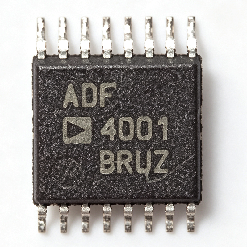
AD4001BRUZ - 16-Bit 2MSPS Differential SAR ADC | Analog Devices
The AD4001BRUZ is a 16-bit, 2 MSPS precision successive approximation register (SAR) analog-to-digital converter (ADC) from Analog Devices. It features a fully differential input, a high-speed serial interface, and operates from a single 1.8 V supply. The device is available in a 16-lead TSSOP package, making it suitable for space-constrained precision data acquisition systems. An ADC (analog-to-digital converter) is an electronic component that converts continuous analog signals into discrete digital values. The AD4001BRUZ is a SAR ADC, which uses a binary search algorithm to determine the digital output. SAR ADCs are known for their high speed, low power, and excellent accuracy, making them ideal for applications such as industrial process control, medical instrumentation, and test and measurement equipment. The AD4001BRUZ is part of the precision ADC family, which includes other high-performance converters from Analog Devices. Key features of the AD4001BRUZ include a 2 MSPS throughput, 16-bit resolution, and a differential input range that can be configured via the reference voltage. The device offers a high signal-to-noise ratio (SNR) and low power consumption, typically 15 mW at 2 MSPS. It also includes an input overvoltage clamp that protects the ADC inputs from overvoltage events, minimizing disturbances on the reference pin and eliminating the need for external protection diodes. The serial interface is SPI-compatible and supports daisy-chaining for multiple ADCs. The AD4001BRUZ uses a precision capacitive DAC architecture with a track-and-hold circuit, ensuring accurate conversion of fast-changing signals. The device operates from a 1.8 V analog supply and a separate digital supply, allowing flexible interfacing with different logic levels. The reference input accepts a wide range of voltages, enabling the user to scale the input span to match the application requirements. The device also features a busy indicator and a conversion result readback that can be synchronized with an external clock. Typical applications for the AD4001BRUZ include industrial automation, data acquisition systems, medical imaging, and portable instrumentation. Its high speed and precision make it suitable for applications that require accurate measurement of dynamic signals, such as vibration analysis and motor control. The small TSSOP package and low power consumption make it ideal for battery-powered devices. When designing with the AD4001BRUZ, it is important to provide a clean, low-noise reference voltage and adequate decoupling on the power supply pins. The input signal should be driven by a low-impedance source, such as an operational amplifier, to ensure accurate conversion. The SPI interface should be configured for the correct clock polarity and phase to match the device's timing requirements.
AD4052BCPZ - 16-Bit 2 MSPS Easy Drive SAR ADC | Analog Devices
The Analog Devices AD4052BCPZ is a compact, low power, 16-bit successive approximation register (SAR) analog-to-digital converter (ADC) capable of operating at up to 2 MSPS in sample mode or 500 kSPS in autonomous mode. The device is supplied in a 14-lead LFCSP (2.0 mm x 2.6 mm) package and is recommended for new designs. It accepts a single analog input and communicates over a robust 4-wire SPI interface with cyclic redundancy check (CRC) support. A SAR ADC is a type of data converter that uses a binary search algorithm to approximate the input voltage with a successively refined comparator and internal digital-to-analog converter. SAR ADCs are widely used in precision data acquisition because they deliver excellent linearity and signal-to-noise performance at high sample rates while consuming relatively low power. In a signal chain, the ADC sits between an analog front-end (e.g., a sensor amplifier) and a digital host such as a microcontroller or FPGA. The AD4052 delivers an integral nonlinearity (INL) of ±0.5 LSB maximum and a signal-to-noise ratio (SNR) of 86.1 dB with VREF = 3.3 V. Its energy efficiency is 1.35 nJ per conversion. At 1 MSPS and 500 kSPS in sample mode, the device consumes 1.35 mW and 0.68 mW respectively; in autonomous modes, power drops to 370 μW at 1 MSPS and 112 μW at 300 kSPS. Standby power is only 4.1 μW, making the AD4052 ideal for battery-powered and intermittently-operated systems. Technically, the AD4052 uses Analog Devices' Easy Drive architecture, which reduces the input driving requirements and simplifies the analog front-end. The device supports power cycling of the voltage reference and can use the power supply itself as VREF to save additional power. The SPI interface supports CRC for all data transfers, enhancing system reliability in electrically noisy environments. Device configuration is performed through register read/write transactions, and a tCONFIG delay is required after an exit command before new SPI transactions may begin. Typical applications include battery-powered IoT sensors, portable medical monitoring, industrial data acquisition, energy-harvesting systems, and precision instrumentation. The combination of 16-bit resolution, 86.1 dB SNR, 1.35 nJ/conversion efficiency, and a tiny 14-lead LFCSP package enables dense, low-power, high-accuracy signal chains. When designing with this converter, pay special attention to reference bypassing, SPI signal integrity, and the tCONFIG timing requirement. A well-decoupled VREF pin with a low-ESR ceramic capacitor is essential to maintain the specified AC performance.
AD4080 - 20-Bit 40 MSPS SAR ADC | Analog Devices
The AD4080 is a high-speed, low noise, low distortion, 20-bit, Easy Drive, successive approximation register (SAR) analog-to-digital converter (ADC) from Analog Devices. It achieves a signal-to-noise and distortion ratio (SINAD) greater than 90 dBFS at signal frequencies up to 40 MSPS, making it ideal for precision, wide-bandwidth data acquisition systems. The device is available in a 49-ball CSPBGA (5x5 mm) package and is recommended for new designs. A SAR ADC is a type of analog-to-digital converter that uses a binary search algorithm to convert an analog input into a digital output. It operates by comparing the input voltage against a series of reference voltages, successively narrowing down the range until the digital code is determined. SAR ADCs are known for their high resolution, low power consumption, and fast conversion times, making them suitable for applications such as medical imaging, industrial process control, and scientific instrumentation. The AD4080 is a high-performance member of this family, offering 20-bit resolution at a high sampling rate. Key features of the AD4080 include Easy Drive technology, which reduces input-dependent signal currents and simplifies the driving amplifier requirements. This feature minimizes converter-induced settling artifacts, allowing for lower power consumption and greater channel density. The device also supports differential input signals, which improves common-mode rejection and reduces noise. With a 40 MSPS throughput, it can capture fast-changing signals with high fidelity. The AD4080 is designed for precision applications where low noise and high linearity are critical. Its 20-bit resolution and >90 dBFS SINAD ensure accurate representation of small signal variations. The device operates from a 1.8 V supply and features a serial LVDS interface for high-speed data transfer. It includes an internal reference buffer and supports external reference options for flexibility. Typical applications include medical imaging systems, such as ultrasound and MRI, where high-resolution data acquisition is essential. It is also used in industrial automation for precise measurement and control, and in scientific instrumentation for capturing high-speed, low-amplitude signals. The AD4080's Easy Drive input structure simplifies the front-end design, reducing component count and board space. When designing with the AD4080, it is important to provide a clean, low-jitter sampling clock to achieve optimal noise performance. The differential input should be driven by a low-noise amplifier with sufficient bandwidth to avoid aliasing. Proper decoupling of the power supply pins and careful PCB layout are essential to minimize noise coupling.
AD4080BCPZ - 20-Bit, 40 MSPS SAR ADC | Analog Devices
The AD4080BCPZ is a high-speed, low noise, low distortion, 20-bit, Easy Drive, successive approximation register (SAR) analog-to-digital converter (ADC) from Analog Devices. It operates at a sampling rate of 40 MSPS and maintains a signal-to-noise and distortion ratio (SINAD) greater than 90 dBFS at signal frequencies in the MHz range. The device features a differential input structure and integrates critical supply and reference decoupling capacitors in the package to simplify PCB layout and reduce solution footprint. The AD4080 is recommended for new designs and is available in a compact LFCSP package. A SAR ADC is a type of analog-to-digital converter that uses a successive approximation register to convert an analog input to a digital output by comparing the input against a binary-weighted reference voltage. SAR ADCs are known for their high resolution, low power consumption, and fast conversion times, making them ideal for applications requiring high-speed, high-precision data acquisition. The AD4080 belongs to the family of precision SAR ADCs, which are essential components in signal processing chains for industrial, medical, and communications systems. Key features of the AD4080 include its 20-bit resolution, 40 MSPS sampling rate, and Easy Drive input structure that minimizes input-dependent signal currents, reducing converter-induced settling artifacts. The continuous acquisition architecture allows settling across multiple conversion cycles, enhancing performance in multiplexed systems. The integrated decoupling capacitors ensure optimal performance without external components, simplifying design and reducing board space. Technically, the AD4080 employs a high-speed SAR architecture with a low-noise comparator and precision DAC, achieving excellent linearity and dynamic performance. The device operates from a single supply and includes a reference buffer, reducing external component count. The Easy Drive feature reduces signal chain complexity and power consumption, enabling greater channel density and flexibility in companion component selection. Typical applications include high-speed data acquisition systems, medical imaging, communications infrastructure, and industrial instrumentation. The AD4080's combination of high resolution, speed, and low noise makes it suitable for demanding measurement and signal processing tasks. When designing with the AD4080, ensure proper decoupling of the supply and reference pins, and follow the recommended layout guidelines in the datasheet to achieve optimal performance. The integrated decoupling capacitors reduce external component requirements, but careful PCB design is still essential for high-speed operation.
AD4080BCPZ-RL7 - 20-Bit, 40 MSPS SAR ADC | Analog Devices
The AD4080BCPZ-RL7 is a high-speed, low-noise, low-distortion, 20-bit successive approximation register (SAR) analog-to-digital converter (ADC) from Analog Devices. It features a differential input, Easy Drive architecture, and a maximum sampling rate of 40 MSPS. The device maintains a signal-to-noise and distortion ratio (SINAD) greater than 90 dBFS at signal frequencies above 1 MHz, making it suitable for precision, wide-bandwidth data acquisition systems. The AD4080BCPZ-RL7 is offered in a 49-ball CSPBGA (5x5 mm) package and is recommended for new designs. A SAR ADC is a type of analog-to-digital converter that uses a binary search algorithm to convert an analog input into a digital output. It operates by comparing the input signal against a reference voltage using a successive approximation register, which narrows down the value bit by bit. SAR ADCs are known for their high resolution, low power consumption, and fast conversion times, making them ideal for applications such as industrial process control, medical imaging, and communications. The AD4080BCPZ-RL7 belongs to the family of precision SAR ADCs, which are essential components in modern data acquisition systems. Key features of the AD4080BCPZ-RL7 include its 20-bit resolution, 40 MSPS sampling rate, and differential input architecture. The Easy Drive design simplifies the input drive requirements, reducing the need for external components. The device also offers low power consumption, making it suitable for battery-powered and portable applications. The high SINAD performance ensures accurate signal reproduction even at high frequencies, which is critical for applications such as radar, lidar, and high-speed instrumentation. From a technical perspective, the AD4080BCPZ-RL7 utilizes a precision SAR architecture with an internal reference and track-and-hold circuit. The device operates from a single 5V supply and features a serial interface for data output. The 49-ball CSPBGA package provides excellent thermal performance and a compact footprint, enabling high-density PCB designs. The ADC also includes a power-down mode to conserve energy during idle periods. Typical applications for the AD4080BCPZ-RL7 include high-speed data acquisition systems, medical imaging equipment, communications infrastructure, and industrial automation. Its combination of high resolution, speed, and low noise makes it an excellent choice for applications that require precise analog-to-digital conversion. The device is also suitable for use in test and measurement instruments, where accuracy and reliability are paramount. When designing with the AD4080BCPZ-RL7, it is important to consider the input signal conditioning and reference voltage stability. Proper decoupling of the power supply and careful PCB layout are essential to achieve the specified performance. The device's Easy Drive feature simplifies the input drive, but attention should be paid to the input common-mode voltage range to ensure optimal operation.
AD4081 - 20-Bit 20MSPS SAR ADC | Analog Devices
The AD4081 is a high-speed, low-noise, low-distortion, 20-bit, Easy Drive, successive approximation register (SAR) analog-to-digital converter (ADC) from Analog Devices. It achieves a signal-to-noise and distortion (SINAD) ratio greater than 90 dBFS at signal frequencies exceeding 1 MHz, making it suitable for precision, wide-bandwidth applications. The device operates as a differential SAR ADC with a maximum sampling rate of 20 MSPS and a latency of 77.50 ns. It is available in a 49-ball CSPBGA (5x5 mm) package, with the specific variant AD4081BBCZ listed on DigiKey. A SAR ADC is a type of analog-to-digital converter that uses a successive approximation register to perform a binary search through all possible quantization levels before converging on the final digital output. This architecture offers a balance of high speed, high resolution, and low power consumption, making SAR ADCs ideal for applications such as data acquisition systems, medical imaging, and industrial process control. The AD4081 belongs to the broader category of data converters, which are essential components in mixed-signal systems that bridge the analog and digital domains. Key features of the AD4081 include its 20-bit resolution, 20 MSPS sampling rate, and Easy Drive input structure that minimizes input-dependent signal currents, reducing converter-induced settling artifacts. The device supports continuous acquisition, which relaxes driver constraints and simplifies the signal chain. Its high SINAD performance at frequencies above 1 MHz enables accurate digitization of wideband signals, making it suitable for applications like radar, communications, and test equipment. Technically, the AD4081 leverages a differential input architecture to reject common-mode noise and improve dynamic range. The Easy Drive feature reduces the need for high-bandwidth, high-power drivers, thereby lowering overall system power consumption and enabling greater channel density. The device's low latency of 77.50 ns is critical for real-time control loops and high-speed feedback systems. Typical applications include high-speed data acquisition, medical ultrasound, industrial automation, and communications infrastructure. The AD4081's combination of high resolution and high speed makes it ideal for digitizing wideband signals with excellent fidelity. When designing with the AD4081, ensure proper decoupling of the power supply pins and careful layout of the analog input traces to maintain signal integrity. The Easy Drive input structure allows for simpler driver design, but attention to reference voltage stability is essential for achieving the specified performance.
AD4083BCPZ - 16-Bit 40MSPS SAR ADC | Analog Devices
The AD4083BCPZ is a high-speed, low-noise, low-power, 16-bit successive approximation register (SAR) analog-to-digital converter (ADC) from Analog Devices. It operates at a maximum sampling rate of 40 MSPS and is designed for applications requiring high resolution and high speed with minimal power consumption. The device features an Easy Drive architecture that simplifies the analog front-end design by reducing input drive requirements. It includes an integrated low-drift reference buffer, low-dropout (LDO) regulators for the ADC core and digital interface supply rails, and a 16K result data FIFO to reduce the load on the digital host. Critical supply and reference decoupling capacitors are integrated in the package, minimizing external component count and board space. An ADC (analog-to-digital converter) is an electronic device that converts a continuous analog signal into a discrete digital representation. The AD4083 is a SAR ADC, which uses a successive approximation algorithm to determine the digital output bit by bit. SAR ADCs are known for their high resolution, low power, and fast conversion times, making them suitable for applications such as medical imaging, communications, and industrial data acquisition. The AD4083 is part of the broader class of data converters, which are essential in bridging the analog and digital domains in electronic systems. Key features of the AD4083 include a signal-to-noise and distortion (SINAD) ratio greater than 90 dBFS, ensuring excellent dynamic performance. The device operates from a single 1.8 V analog supply and a 1.8 V digital interface supply, with power dissipation typically below 100 mW at 40 MSPS. The integrated LDO regulators allow the ADC to generate its own internal supply rails, simplifying power supply design. The 16K FIFO reduces the need for high-speed data transfer to the host processor, enabling efficient data capture in burst-mode applications. The AD4083 is available in a 49-ball CSPBGA (5x5 mm) package, which is compact and suitable for space-constrained designs. The device is specified for operation over the industrial temperature range of -40°C to +125°C. It is recommended for new designs, indicating active lifecycle status. The AD4083 is ideal for applications such as medical ultrasound, radar systems, and high-speed data acquisition, where high resolution and low power are critical. When designing with the AD4083, it is important to provide a clean, low-noise analog supply and a stable reference voltage. The integrated LDO regulators help, but external decoupling is still recommended. The Easy Drive architecture reduces the need for a high-bandwidth input driver, but a suitable driver amplifier may still be required for optimal performance. The FIFO can be used to buffer data and reduce the interrupt load on the host processor.
AD4084 - 16-Bit 20 MSPS SAR ADC | Analog Devices
The AD4084 is a 16-bit, 20 MSPS successive approximation register (SAR) analog-to-digital converter (ADC) from Analog Devices, featuring a differential input and Easy Drive technology. It is designed for high-speed, low-noise, low-distortion precision data acquisition, delivering excellent dynamic performance while simplifying the signal chain. The device is available in a 49-ball CSPBGA (5x5 mm) package, suitable for space-constrained industrial and communications systems. A SAR ADC is a type of analog-to-digital converter that uses a binary search algorithm to convert an analog input into a digital output. It typically offers high resolution, low power consumption, and fast conversion times, making it ideal for applications requiring a balance between speed and precision. The AD4084 belongs to the ADC family, which falls under data converters, a subset of analog-to-digital converters, and ultimately within the broader category of mixed-signal integrated circuits. Key features of the AD4084 include 16-bit resolution, a 20 MSPS sampling rate, and a differential input structure that reduces common-mode noise. The Easy Drive technology minimizes input-dependent signal currents, reducing converter-induced settling artifacts and enabling simpler driver circuitry. The device also integrates digital filtering, which enhances dynamic range and simplifies post-processing. With a 1ku list price starting at $31.68, it offers a cost-effective solution for high-performance data acquisition. Technically, the AD4084 employs a precision SAR architecture with an internal reference and track-and-hold circuit, achieving high linearity and low noise. The differential input provides excellent common-mode rejection, while the Easy Drive input structure reduces the need for external high-bandwidth drivers, lowering system power and complexity. The device operates from a single supply and supports a wide input range, making it versatile for various signal levels. Typical applications include industrial process control, medical imaging, communications infrastructure, and test and measurement equipment. In these systems, the AD4084's combination of speed, resolution, and low noise ensures accurate digitization of fast, small-amplitude signals. Its Easy Drive feature is particularly beneficial in multi-channel systems where channel density and power efficiency are critical. When designing with the AD4084, ensure proper decoupling of the power supply and reference pins, and consider the input drive requirements to fully exploit the Easy Drive benefits. The differential input should be driven with a low-impedance source to maintain performance. Additionally, the digital interface should be isolated from noisy logic to prevent coupling into the analog section.
AD4086BCPZ - 14-Bit 40 MSPS SAR ADC | Analog Devices
The AD4086BCPZ is a 14-bit, 40 MSPS successive approximation register (SAR) analog-to-digital converter from Analog Devices, offered in a compact LFCSP package. It is recommended for new designs and integrates a low drift reference buffer, low-dropout (LDO) regulators for the ADC core and digital interface supply rails, a 16K result data FIFO, and internal supply/reference decoupling capacitors. These features simplify data converter integration and reduce external component count. What is a SAR ADC? A SAR ADC converts an analog input into a digital code by performing a binary search across a capacitor DAC under control of a successive-approximation register. SAR ADCs are favored for high-speed, low-power precision data acquisition where low latency and a single-cycle sample-and-hold are important. Within the ADC hierarchy, SAR converters sit between delta-sigma devices and pipeline converters in the speed-versus-resolution trade-off. The AD4086's 14-bit resolution and 40 MSPS throughput make it suitable for applications that require high dynamic range at speed. The integrated 16K FIFO reduces host-side interrupt loading, while the internal LDOs and reference buffer lower external BOM count. Low noise and low power design support dense, channel-count systems. Because critical supply and reference decoupling capacitors are integrated inside the package, PCB layout is simplified and parasitic inductance from external decoupling is minimized. The LDOs generate clean core and digital rails, reducing the need for multiple external regulators. The low drift reference buffer maintains ADC accuracy across temperature. Typical applications include medical imaging front ends, high-speed data acquisition, communications receivers, industrial instrumentation, and portable test equipment. The 40 MSPS rate can address IF/baseband sampling in communications, while low power supports battery-operated units. When designing with the AD4086, pay attention to the input drive amplifier settling time and the reference source impedance. The integrated 16K FIFO should be used to burst-read conversion results to minimize digital host overhead. Ensure the input common-mode range matches the driver output for optimum SNR/SFDR.
AD4130-4BCPZ - 24-Bit Ultra-Low Power Sigma-Delta ADC | Analog Devices
The AD4130-4BCPZ is a 24-bit, ultra-low power, sigma-delta analog-to-digital converter (ADC) from Analog Devices, designed for high-precision, low-frequency measurement applications. It integrates a programmable gain amplifier (PGA), a crosspoint multiplexer, a smart sequencer, and a deep FIFO, all in a compact 32-lead LFCSP (5x5 mm) package. Operating from a single analog supply of 1.71 V to 3.6 V, it achieves a current consumption of only 28.5 μA at gain = 1 and 32.5 μA at gain = 128 while continuously converting, making it ideal for battery-powered and loop-powered systems. An ADC (analog-to-digital converter) is a device that converts continuous analog signals into discrete digital numbers. The AD4130-4 is a sigma-delta ADC, which uses oversampling and noise shaping to achieve high resolution (24 bits) and excellent noise performance for low-bandwidth signals. It belongs to the family of precision data converters, which are essential in industrial process control, medical instrumentation, and smart sensor nodes. The integration of a PGA and multiplexer reduces external component count and simplifies system design. Key features include 4 differential or 8 single-ended/pseudo-differential inputs, a crosspoint multiplexer that allows any input pair to be routed to the PGA and ADC, and built-in diagnostic functions such as open-wire detection, internal temperature sensor, reference detection, and analog input overvoltage/undervoltage detection. The device also supports duty cycling modes (1/4 or 1/16) to reduce average current to as low as 5 μA, and a standby mode at 0.5 μA and power-down mode at 0.1 μA. The AD4130-4 uses a 24-bit sigma-delta modulator with a digital filter, providing high accuracy and noise rejection. The smart sequencer and per-channel configuration minimize host processor load, while the deep 256-sample FIFO allows autonomous data collection. The SPI interface enables easy integration with microcontrollers. The device is specified for operation from -40°C to +125°C, suitable for industrial environments. Typical applications include industrial process control (4-20 mA loops), temperature and pressure measurement, battery monitoring, and portable medical devices. Its ultra-low power consumption and integrated diagnostics make it particularly suited for smart transmitters and IoT sensor nodes. When designing with the AD4130-4, ensure proper decoupling of the analog supply and reference pins, and use a clean ground plane to minimize noise. The SPI interface should be isolated if used in noisy industrial environments.
AD4170BCPZ - 24-Bit Sigma-Delta ADC, 500kSPS | Analog Devices
The AD4170BCPZ is a high-speed, low-noise, 24-bit sigma-delta analog-to-digital converter (ADC) from Analog Devices, designed for precision measurement applications requiring DC to 50 kHz input bandwidth. It supports output data rates from 7.6 SPS up to 500 kSPS, making it suitable for both low-speed high-resolution and high-speed data acquisition systems. The device is available in a 32-lead LFCSP (4x6 mm) package, offering a compact solution for space-constrained designs. A sigma-delta ADC is a type of analog-to-digital converter that uses oversampling and noise shaping to achieve high resolution. It is widely used in precision measurement, industrial process control, and medical instrumentation where accuracy and low noise are critical. The AD4170BCPZ integrates a low-noise programmable gain amplifier (PGA) and a precision voltage reference, reducing external component count and simplifying system design. Key features include a 24-bit resolution, 8 input channels (configurable as 4 differential or 8 single-ended), and a maximum output data rate of 500 kSPS. The device offers a low noise floor, enabling accurate measurement of small signals. It also includes a flexible digital filter, allowing users to trade off between speed and noise performance. The integrated PGA provides gain settings from 1 to 128, accommodating a wide range of sensor outputs. The AD4170BCPZ operates from a 2.5V to 5.5V analog supply and a 1.8V to 5.5V digital interface supply, ensuring compatibility with modern microcontrollers and DSPs. It features a serial peripheral interface (SPI) for communication, supporting both 3-wire and 4-wire modes. The device also includes a reference detect function and a temperature sensor, enhancing its versatility in system monitoring applications. Typical applications include precision weigh scales, strain gauge measurements, thermocouple and RTD temperature sensing, and industrial process control. The high output data rate and low noise make it ideal for vibration analysis and high-speed data acquisition systems. The device's integrated features reduce board space and bill of materials, making it a cost-effective solution for precision measurement. When designing with the AD4170BCPZ, ensure proper decoupling of the analog and digital supplies to minimize noise coupling. The reference input should be bypassed with a low-ESR capacitor to maintain stability. The SPI interface should be isolated from noisy digital traces to preserve the ADC's noise performance.
AD4851BCPZ - 16-Bit 4-Ch Simultaneous Sampling DAS | Analog Devices
The AD4851BCPZ is a fully buffered, 4-channel simultaneous sampling, 16-bit, 250kSPS data acquisition system (DAS) from Analog Devices. It integrates four internal buffer amplifiers, a 16-bit SAR ADC, an internal 4.096V reference and reference buffer, and supply decoupling capacitors, all in a compact 64-ball BGA (7x7 mm) package. Operating from a single 5V supply, it delivers 36mW per channel at 250kSPS, scaling with throughput. The device features differential, wide common-mode range inputs with ±75pA typical input leakage at 25°C and full-scale input step settling time of less than 300ns. A data acquisition system (DAS) is a complete signal chain that conditions, samples, and converts analog signals to digital words. The AD4851 integrates the input buffer, ADC, and reference, reducing external component count and simplifying design. It sits within the hierarchy: DAS -> ADC -> data converter -> mixed-signal IC -> semiconductor. This integration is critical for multi-channel systems where board space and channel-to-channel matching are paramount. Key features include simultaneous sampling of four channels, ensuring phase-accurate capture of multi-phase signals, and a wide common-mode input range that accommodates various sensor outputs without external level shifting. The integrated reference and buffer eliminate the need for external reference circuitry, while internal supply decoupling capacitors reduce external bypass requirements. The device operates over the industrial temperature range and is recommended for new designs. Architecturally, the AD4851 uses a successive approximation register (SAR) architecture, offering a balance of speed, resolution, and power. The internal buffers present a high-impedance input to the sensor, minimizing loading and preserving signal integrity. The wide common-mode range allows direct connection to differential signals with large offsets, simplifying front-end design. The 250kSPS per channel throughput supports high-speed industrial and instrumentation applications. Typical applications include motor control (phase current and voltage sensing), power monitoring, vibration analysis, and multi-phase power quality measurement. The simultaneous sampling capability is essential for accurate power calculations in three-phase systems. The device's low power and small footprint make it suitable for portable and space-constrained designs. When designing with the AD4851, ensure adequate decoupling on the supply pins and a clean reference voltage. The internal reference is 4.096V, but an external reference can be used if higher accuracy is required. The SPI interface simplifies connection to microcontrollers and DSPs. Careful PCB layout, with short analog input traces and a solid ground plane, is essential to achieve the specified performance.
AD4852BCPZ - 20-Bit 250kSPS 4-Ch DAS | Analog Devices
The AD4852BCPZ from Analog Devices is a fully buffered, 4-channel simultaneous sampling, 20-bit, 250kSPS data acquisition system (DAS) with differential, wide common-mode range inputs. It integrates a complete signal chain including input buffers, a 20-bit SAR ADC, an internal reference and reference buffer, and supply decoupling capacitors, all in a compact 64-lead LFCSP package. Operating from a 5V low-voltage supply, it delivers 36mW per channel at 250kSPS, scaling with throughput for power-efficient designs. A data acquisition system (DAS) is a complete signal chain that conditions, samples, and converts analog signals into digital data. The AD4852 integrates the analog front-end, ADC, and reference, simplifying design and reducing component count. It sits within the hierarchy: DAS -> ADC -> data converter -> mixed-signal IC -> semiconductor. This integration is critical for high-channel-count systems where board space and power are at a premium. Key features include ±75pA typical input leakage at 25°C, full-scale input step settling time of less than 300ns, and an integrated 4.096V reference. The differential inputs with wide common-mode range allow direct connection to sensors and transducers without external conditioning. The device also features a flexible digital interface supporting SPI and daisy-chain modes, enabling multiple devices to be cascaded for higher channel counts. Technically, the AD4852 uses a successive approximation register (SAR) architecture with internal buffering, eliminating the need for external driver amplifiers. The integrated reference buffer ensures stable and accurate conversions over temperature. The device includes a temperature sensor and a 1.024V output for system diagnostics. Its power dissipation scales with throughput, making it suitable for battery-powered and thermal-constrained applications. Typical applications include industrial automation, motor control, power line monitoring, and multi-phase energy metering. The simultaneous sampling capability is essential for applications requiring phase-accurate measurements across multiple channels, such as three-phase power monitoring and vibration analysis. The wide common-mode input range and high input impedance simplify sensor interfacing. When designing with the AD4852, ensure adequate decoupling on the AVDD and DVDD supplies, and use the integrated reference buffer to drive the reference input. The device supports a 1.8V to 5V digital interface, allowing direct connection to modern microcontrollers and FPGAs. For optimal performance, follow the layout guidelines in the datasheet, including a solid ground plane and minimal trace lengths on the analog inputs.