ADC/DAC
Products (181)
AD7385BCPZ - 16-Bit Quad SAR ADC | Analog Devices
The AD7385BCPZ is a 16-bit, quad-channel, simultaneous sampling, successive approximation register (SAR) analog-to-digital converter (ADC) from Analog Devices. It operates from a 3.0 V to 3.3 V power supply and features a high-speed serial peripheral interface (SPI) for data transfer. The device is available in a compact 24-lead LFCSP (4x4 mm) package, making it suitable for space-constrained industrial and automotive applications. An ADC (analog-to-digital converter) is an electronic component that converts continuous analog signals into discrete digital values. The AD7385BCPZ is a SAR ADC, which uses a binary search algorithm to approximate the input voltage with high speed and accuracy. SAR ADCs are widely used in applications requiring a balance of speed, resolution, and power efficiency, such as motor control, power monitoring, and data acquisition systems. The AD7385BCPZ belongs to the family of high-speed, low-power ADCs from Analog Devices, which are known for their excellent AC performance and ease of use. Key features of the AD7385BCPZ include 16-bit resolution, four simultaneously sampled input channels, and a maximum sampling rate of 2 MSPS (megasamples per second). The device supports both external and internal reference options, and includes a built-in FIFO buffer and soft reset functionality. It also features a power-on reset and simultaneous sampling capability, which is essential for applications that require accurate phase alignment between multiple channels. The ADC achieves a signal-to-noise ratio (SNR) of 86.7 dB and a total harmonic distortion (THD) of -100 dB, ensuring high-fidelity signal conversion. From a technical perspective, the AD7385BCPZ integrates a precision reference buffer and a high-speed SPI interface that supports daisy-chaining for multiple devices. The device operates over a temperature range of -40°C to +125°C, making it suitable for harsh environments. The LFCSP package provides excellent thermal performance and a small footprint, enabling high-density PCB layouts. The ADC's low power consumption of 200 µA in standby mode makes it ideal for battery-powered and energy-efficient designs. Typical applications for the AD7385BCPZ include motor control, power monitoring, data acquisition systems, and industrial automation. In motor control, the simultaneous sampling capability ensures accurate current and voltage measurements for precise control loops. In power monitoring, the high resolution and fast sampling rate enable accurate measurement of AC and DC power parameters. The device is also well-suited for vibration analysis and other condition monitoring applications where multi-channel synchronization is critical. When designing with the AD7385BCPZ, it is important to provide a clean, low-noise power supply and proper decoupling to achieve optimal performance. The reference input should be bypassed with a 10 µF capacitor to ensure stability. Additionally, the SPI interface should be routed with controlled impedance to minimize signal integrity issues at high data rates.
AD7386BCPZ - 16-Bit 4MSPS Dual SAR ADC | Analog Devices
The AD7386BCPZ is a 16-bit, dual, simultaneous sampling, high-speed successive approximation register (SAR) analog-to-digital converter (ADC) from Analog Devices. It operates from a 3.0 V to 3.6 V power supply and features throughput rates of up to 4 MSPS. The device includes two SAR ADCs, a multiplexer, a sequencer, and a serial interface with two separate data output pins, all housed in a compact 16-lead LFCSP (3x3 mm) package. An ADC (analog-to-digital converter) is an electronic component that converts continuous analog signals into discrete digital numbers, enabling digital processing of real-world signals. SAR ADCs use a successive approximation register algorithm to perform conversions with high speed and excellent accuracy, making them ideal for applications requiring precise, fast measurements. The AD7386 belongs to the precision ADC family, which is a subset of data converters within the broader analog-to-digital conversion hierarchy. Key features of the AD7386BCPZ include dual simultaneous sampling, which allows two channels to be sampled at the exact same instant, preserving phase relationships between signals. The integrated multiplexer and sequencer enable automatic scanning of multiple input channels without external control. The serial interface with two data output pins supports high-speed data transfer while simplifying the connection to microcontrollers or DSPs. The device also offers a wide input bandwidth and low power consumption, making it suitable for portable and battery-powered applications. Technically, the AD7386 uses a precision capacitor-based DAC and a high-speed comparator to achieve 16-bit resolution with no missing codes. The device features a flexible power-down mode to reduce current consumption between conversions, and it supports both SPI and QSPI interfaces. The LFCSP package provides excellent thermal performance and a small footprint, ideal for space-constrained designs. Typical applications include motor control, power monitoring, data acquisition systems, and industrial automation. In motor control, the dual simultaneous sampling capability is critical for accurate current and voltage measurement. In power monitoring, the high throughput and resolution enable precise energy metering. The device's small size and low power make it suitable for portable instrumentation. When designing with the AD7386BCPZ, ensure proper decoupling of the power supply pins with 0.1 uF and 10 uF capacitors placed close to the device. The reference input should be driven by a low-impedance source to maintain accuracy. The serial interface timing must be carefully matched to the host controller to avoid data corruption.
AD7387BCPZ - 14-Bit Dual SAR ADC 4MSPS | Analog Devices
The AD7387BCPZ is a 14-bit, dual, simultaneous sampling, high-speed successive approximation register (SAR) analog-to-digital converter (ADC) from Analog Devices. It operates from a 3.0 V to 3.6 V power supply and features a throughput rate of 4 MSPS per channel. The device is available in a 16-lead LFCSP (3x3 mm) package, making it suitable for space-constrained industrial and instrumentation applications. A SAR ADC is a type of analog-to-digital converter that uses a binary search algorithm to convert an analog input into a digital output. It is known for its high speed, low power consumption, and ease of use compared to other ADC architectures like delta-sigma or pipeline converters. SAR ADCs are widely used in applications requiring high resolution and fast sampling, such as motor control, data acquisition, and power monitoring. Key features of the AD7387BCPZ include a 4-channel input with 2:1 multiplexers, a built-in digital filter, FIFO buffer, soft reset, and power-on reset. It supports simultaneous sampling of two channels, which is essential for applications that require accurate phase alignment between multiple signals. The device also features a channel sequencer mode for automatic scanning of multiple input channels. The AD7387BCPZ uses a high-speed SAR architecture with an internal reference and track-and-hold circuit. It provides a serial interface (SPI) for communication with microcontrollers or DSPs. The device includes a built-in digital filter to reduce noise and improve signal-to-noise ratio (SNR). The FIFO buffer allows for efficient data transfer without overloading the host processor. Typical applications include motor control, industrial automation, data acquisition systems, and power monitoring. The simultaneous sampling capability makes it ideal for three-phase motor control where accurate current and voltage measurements are required. The wide operating temperature range of -40°C to +125°C ensures reliable operation in harsh environments. When designing with the AD7387BCPZ, ensure that the analog input signals are properly conditioned with anti-aliasing filters to avoid aliasing. The reference voltage should be stable and low-noise to achieve the specified SNR. The SPI interface should be isolated if the ADC is used in noisy industrial environments.
AD7388BCPZ - 12-Bit 4MSPS Dual SAR ADC | Analog Devices
The AD7388BCPZ is a 12-bit, dual, simultaneous sampling, successive approximation register (SAR) analog-to-digital converter (ADC) from Analog Devices. It operates from a 3.0 V to 3.6 V power supply and features a throughput rate of 4 MSPS per channel. The device is available in a 16-lead LFCSP (3x3 mm) package, making it suitable for space-constrained industrial and instrumentation applications. An ADC (analog-to-digital converter) is an electronic component that converts continuous analog signals into discrete digital values. The AD7388BCPZ is a SAR ADC, which uses a binary search algorithm to determine the digital output. SAR ADCs are known for their high speed, low power consumption, and excellent accuracy, making them ideal for applications such as motor control, data acquisition, and power monitoring. The AD7388BCPZ is part of the AD7386/AD7387/AD7388 family, which includes 16-bit, 14-bit, and 12-bit versions, respectively. Key features of the AD7388BCPZ include dual simultaneous sampling, which allows two channels to be sampled at the same time, preserving phase information between signals. The device also features a high-speed serial interface (SPI) that supports daisy-chaining, enabling multiple ADCs to be connected to a single microcontroller. The ADC includes an internal reference and reference buffer, reducing external component count. The input range is configurable, supporting both single-ended and differential inputs, with a common-mode voltage range that simplifies signal conditioning. The AD7388BCPZ uses a charge redistribution architecture with a capacitive DAC, providing excellent linearity and low noise. The device achieves a signal-to-noise ratio (SNR) of 72 dB and a total harmonic distortion (THD) of -80 dB, ensuring high-fidelity conversion. The ADC also features a flexible power-down mode, reducing power consumption to 3 mW at lower throughput rates. The SPI interface supports multiple operating modes, including a turbo mode for maximum throughput and a reduced power mode for lower data rates. Typical applications for the AD7388BCPZ include motor control, where simultaneous sampling of current and voltage is critical for accurate torque control; data acquisition systems, where high speed and accuracy are required; and power monitoring, where the ADC can measure multiple phases simultaneously. The device is also suitable for industrial automation, test and measurement, and medical instrumentation. When designing with the AD7388BCPZ, it is important to provide a clean, low-noise power supply and to decouple the AVDD and DVDD pins with 0.1 uF and 10 uF capacitors. The reference pin should be bypassed with a 10 uF capacitor to ensure stable operation. The SPI interface should be kept short and properly terminated to avoid signal integrity issues at high data rates.
AD7389BCPZ - 16-Bit Quad SAR ADC 2MSPS | Analog Devices
The AD7389BCPZ is a 16-bit, quad, simultaneous sampling, high-speed successive approximation register (SAR) analog-to-digital converter (ADC) from Analog Devices. It operates from a 3.0 V to 3.6 V power supply and features throughput rates up to 2 MSPS. The analog input type is differential, accepts a wide common-mode input voltage, and the analog inputs are sampled and converted on the falling edge of the conversion signal. The device is available in a 24-lead LFCSP (4x4 mm) package, making it suitable for space-constrained industrial and instrumentation applications. A SAR ADC is a type of analog-to-digital converter that uses a binary search algorithm to convert an analog input into a digital output. It is known for its high speed, low power consumption, and excellent accuracy. SAR ADCs are widely used in applications such as motor control, data acquisition systems, and industrial automation, where precise and fast conversion is required. The AD7389BCPZ is part of the AD7389-4 family, which includes quad-channel, simultaneous sampling SAR ADCs with internal reference and differential inputs. Key features of the AD7389BCPZ include 16-bit resolution, 2 MSPS throughput, quad differential inputs, internal reference, and simultaneous sampling. The device also features a wide common-mode input voltage range, making it ideal for applications with varying input signal levels. The internal reference eliminates the need for an external reference, simplifying the design and reducing component count. The device operates from a single 3.3 V supply, making it compatible with modern digital systems. The AD7389BCPZ uses a SAR architecture with a capacitive DAC and a comparator, achieving high accuracy and low power consumption. The device includes a track-and-hold circuit that samples all four channels simultaneously, ensuring accurate phase alignment between channels. The digital interface is SPI-compatible, allowing easy connection to microcontrollers and DSPs. The device also features a busy indicator and a conversion result readback, simplifying the data acquisition process. Typical applications for the AD7389BCPZ include motor control, power monitoring, data acquisition systems, and industrial automation. The device is also suitable for medical instrumentation and test and measurement equipment, where high accuracy and speed are critical. The wide common-mode input range and differential inputs make it ideal for bridge sensors and other differential signal sources. When designing with the AD7389BCPZ, ensure that the power supply is well decoupled and that the reference voltage is stable. The device requires a clean analog supply and a separate digital supply to minimize noise coupling. The SPI interface should be properly terminated to avoid signal integrity issues. The device is available in a 24-lead LFCSP package, which provides good thermal performance and is suitable for compact PCB layouts.
AD7390BCPZ - 12-Bit Serial DAC, 3V Supply | Analog Devices
The AD7390BCPZ is a 12-bit voltage-output digital-to-analog converter (DAC) from Analog Devices, designed for single +3 V supply operation. It is built on a CBCMOS process, offering low cost and ease-of-use in single-supply systems. The device operates over a supply range of +2.7 V to +5.5 V while consuming less than 100 µA, making it ideal for battery-powered and portable applications. The AD7390BCPZ comes in a compact 8-lead LFCSP package, providing a small footprint for space-constrained designs. A digital-to-analog converter (DAC) is an electronic component that converts digital binary data into an analog voltage or current. The AD7390 is a voltage-output DAC, meaning it directly outputs a voltage proportional to the digital input code. It is part of the broader family of data converters, which also includes analog-to-digital converters (ADCs). DACs are essential in systems where digital processing must interface with the analog world, such as audio playback, motor control, and sensor calibration. Key features of the AD7390BCPZ include 12-bit resolution, a serial interface compatible with SPI/QSPI/MICROWIRE, and a buffered output that can drive capacitive loads. The device includes a power-on reset that clears the output to zero scale, ensuring predictable startup behavior. The low supply current of less than 100 µA extends battery life in portable devices. The LFCSP package is lead-free and RoHS compliant, meeting modern environmental standards. Technically, the AD7390 uses a resistor-string architecture with an output buffer amplifier. The serial interface allows easy connection to microcontrollers and DSPs with minimal pin count. The device supports a wide operating temperature range of -40°C to +85°C, suitable for industrial environments. The output voltage range is 0 V to VREF, where VREF can be set externally up to the supply voltage. The DAC's settling time is typically 10 µs, enabling moderate-speed applications. Typical applications include digital gain and offset adjustment, programmable voltage references, and industrial process control. In portable instrumentation, the low power consumption is critical for extending battery life. The AD7390BCPZ is also used in automotive electronics for sensor calibration and in communication systems for bias control. When designing with the AD7390BCPZ, ensure that the reference voltage is stable and well-decoupled to achieve full 12-bit accuracy. The serial clock should be kept clean to avoid data corruption. The output buffer can drive up to 100 pF capacitive load without oscillation, but for larger loads, an external buffer may be required.
AD7391BCPZ - 10-Bit Serial DAC | Analog Devices | 32-LFCSP
The AD7391BCPZ is a 10-bit voltage-output digital-to-analog converter (DAC) from Analog Devices, designed for single-supply operation from +2.7 V to +5.5 V. It features a serial interface, micropower consumption of less than 100 µA, and is available in a 32-lead LFCSP-VQ (5x5 mm) package. This device is part of the AD7390/AD7391 family, which also includes a 12-bit version (AD7390). Built using a CBCMOS process, the AD7391 offers low cost and ease-of-use in single-supply +3 V systems. A digital-to-analog converter (DAC) is an electronic component that converts digital binary data into an analog voltage or current. The AD7391 is a voltage-output DAC, meaning it directly outputs a voltage proportional to the digital input. It is a key building block in many systems, bridging the digital domain of microcontrollers and DSPs with the analog world of sensors, actuators, and audio amplifiers. In the hierarchy of signal chain components, a DAC is part of the data converter family, which also includes ADCs (analog-to-digital converters). Key features of the AD7391BCPZ include its 10-bit resolution, serial interface (SPI-compatible), and low power consumption. The device operates from a single +2.7 V to +5.5 V supply, making it ideal for battery-powered and portable applications. It also features a power-down mode that reduces current consumption to a few microamperes, further extending battery life. The output is buffered, providing a low-impedance drive capability. Technically, the AD7391 uses a resistor-string architecture with a rail-to-rail output buffer. This architecture ensures monotonicity and low differential nonlinearity (DNL). The serial interface allows easy connection to microcontrollers and DSPs with minimal pin count. The device is specified over the industrial temperature range of -40°C to +85°C, making it suitable for a wide range of environments. Typical applications include portable instrumentation, battery-powered data acquisition systems, digital gain and offset adjustment, and programmable voltage references. Its low power and small package make it ideal for space-constrained designs. When designing with the AD7391, ensure that the reference voltage is stable and well-decoupled. The output buffer can drive capacitive loads, but for best settling time, keep the load capacitance below 100 pF. Also, use a clean digital supply to avoid noise coupling into the analog output.
AD7392BCPZ - 12-Bit Serial DAC | Analog Devices
The AD7392BCPZ is a 12-bit digital-to-analog converter (DAC) from Analog Devices, featuring a serial interface and a compact 20-lead LFCSP package. It operates from a single 2.7V to 5.5V supply, making it suitable for battery-powered and portable applications. The device includes an internal reference and output amplifier, providing a rail-to-rail output swing. With a typical settling time of 10 µs, it is designed for precision control and signal generation. A digital-to-analog converter (DAC) is an electronic component that converts digital binary data into an analog voltage or current. DACs are essential in systems where digital processing must interface with the analog world, such as audio playback, motor control, and sensor calibration. The AD7392BCPZ belongs to the family of serial-input DACs, which use a simple SPI-compatible interface to minimize pin count and simplify PCB layout. This device is part of Analog Devices' precision DAC portfolio, known for high accuracy and low power consumption. Key features of the AD7392BCPZ include 12-bit resolution, a maximum output voltage of VREF (which can be set up to VDD), and a power-down mode that reduces current consumption to 1 µA. The device also offers a clear pin for resetting the output to zero scale, and a reference input that can be driven by an external reference or the internal 2.5V reference. The LFCSP package measures 4mm x 4mm, providing a small footprint for space-constrained designs. Technically, the AD7392BCPZ uses a resistor-string architecture, which ensures monotonicity and low differential nonlinearity (DNL) of ±0.5 LSB. The serial interface is compatible with SPI, QSPI, and MICROWIRE protocols, allowing easy connection to microcontrollers and DSPs. The device operates over a temperature range of -40°C to +85°C, making it suitable for industrial environments. Typical applications include programmable voltage sources, digital gain and offset adjustment, and industrial process control. In portable instrumentation, the low power consumption and small package are critical advantages. The device can also be used in closed-loop servo control systems where precise analog output is required. When designing with the AD7392BCPZ, ensure that the reference voltage is stable and that decoupling capacitors are placed close to the VDD and REF pins. The power-down mode can be used to conserve energy in battery-operated systems, but note that the output will be high-impedance in this mode.
AD7393BCPZ - 12-Bit 3V DAC | Analog Devices | LFCSP-40
The AD7393BCPZ is a 12-bit voltage-output digital-to-analog converter (DAC) from Analog Devices, designed for single-supply 3 V systems. It operates over a supply range of 2.7 V to 5.5 V, making it ideal for battery-powered and portable applications. The device is built using a CBCMOS process, offering low cost and ease of use. It is pin-compatible with the AD7392 (10-bit) and AD7393 (12-bit) family, allowing straightforward upgrades. The AD7393BCPZ comes in a 40-lead LFCSP-VQ (6x6 mm) package, which is compact and suitable for space-constrained designs. A digital-to-analog converter (DAC) is an electronic circuit that converts digital binary data into an analog voltage or current. The AD7393 is a voltage-output DAC, meaning it directly produces an analog voltage proportional to the digital input code. It is part of the broader category of data converters, which also includes ADCs (analog-to-digital converters). DACs are essential in systems where digital processing must interface with the analog world, such as audio playback, motor control, and instrumentation. The AD7393's single-supply operation simplifies power supply design, reducing system cost and complexity. Key features of the AD7393BCPZ include 12-bit resolution, a 2.7 V to 5.5 V supply range, and a voltage output that is rail-to-rail. It has a typical settling time of 10 µs, ensuring fast response in dynamic applications. The device includes a power-on reset that clears the output to zero scale, preventing glitches during power-up. It also features a low power consumption of typically 1.5 mW at 3 V, making it suitable for battery-powered devices. The LFCSP-40 package provides excellent thermal performance and a small footprint. Technically, the AD7393 uses a resistor-string architecture with a CMOS switch tree, providing monotonic performance and low glitch energy. The CBCMOS process combines bipolar and CMOS transistors, optimizing speed and power. The device has a maximum output voltage of VREF, which can be set externally or tied to the supply. It includes a reference input that can be driven by an external reference or the supply voltage. The digital interface is a simple parallel input, compatible with standard logic levels. Typical applications for the AD7393BCPZ include portable instrumentation, battery-powered data acquisition systems, and programmable voltage sources. Its low power and small package make it ideal for handheld devices, while its 12-bit resolution suits precision control loops. The device is also used in industrial process control and medical devices where a stable, accurate analog output is required. When designing with the AD7393BCPZ, ensure that the reference voltage is stable and well-decoupled to achieve full accuracy. The output can drive capacitive loads up to 100 pF without external compensation. For best performance, place decoupling capacitors close to the supply and reference pins.
AD7394BCPZ - 12-Bit Serial DAC | Analog Devices
The AD7394BCPZ is a 12-bit digital-to-analog converter (DAC) from Analog Devices, featuring a serial interface and dual-channel output. It operates from a single 2.7V to 5.5V supply, making it suitable for battery-powered and portable applications. The device is available in a compact 20-lead LFCSP package, offering a space-saving solution for precision analog output generation. A digital-to-analog converter (DAC) is an electronic component that converts digital binary data into an analog voltage or current. DACs are essential in systems where digital processing must interface with the analog world, such as audio playback, motor control, and sensor calibration. The AD7394BCPZ belongs to the family of serial-input DACs, which use a simple SPI-compatible interface to receive data, reducing pin count and simplifying PCB layout compared to parallel-input DACs. Key features of the AD7394BCPZ include 12-bit resolution, dual buffered outputs, and a rail-to-rail output swing. It offers a typical settling time of 10 microseconds, ensuring fast response in control loops. The device also includes a power-on reset circuit that sets the output to zero scale, preventing unwanted transients during power-up. Its low power consumption, typically 1.5 mA, is ideal for power-sensitive designs. Technically, the AD7394BCPZ uses a resistor-string architecture with an internal output buffer, providing monotonic performance and low glitch energy. The serial interface supports daisy-chaining, allowing multiple DACs to be controlled with a single chip-select line. The device is specified over the industrial temperature range of -40°C to +85°C, ensuring reliable operation in harsh environments. Typical applications include programmable voltage sources, digital gain and offset adjustment, and industrial process control. In audio systems, it can be used for volume control or tone adjustment. Its small footprint and low power make it suitable for portable instrumentation and battery-operated devices. When designing with the AD7394BCPZ, ensure that the reference voltage is stable and adequately decoupled. The output buffer can drive capacitive loads up to 100 pF without oscillation, but larger loads may require an external buffer. Proper layout with a solid ground plane is recommended to minimize noise and achieve full 12-bit accuracy.
AD74416HBCPZ - Quad Channel Flexible I/O with HART | Analog Devices
The AD74416HBCPZ is a quad-channel, software-configurable input/output (I/O) device from Analog Devices, designed for industrial process control and smart transmitter applications. It integrates four channels that can be independently configured as analog input (voltage or current), analog output (voltage or current), digital input, or digital output, all controlled via a serial peripheral interface (SPI). The device features a 16-bit resolution and supports a data rate of 19.2 kSPS, making it suitable for high-precision measurement and control loops. It is housed in a 64-lead LFCSP (9x9 mm) package, offering a compact solution for space-constrained industrial modules. A software-configurable I/O (SIO) device is a versatile analog front-end that replaces multiple discrete components (e.g., ADCs, DACs, op-amps, and protection circuits) with a single programmable IC. It sits within the data acquisition subsystem of a programmable logic controller (PLC) or distributed control system (DCS), bridging field sensors/actuators to the digital control core. By reconfiguring each channel via software, the same hardware can handle diverse signal types, reducing BOM cost and board area while simplifying inventory management. Key features of the AD74416HBCPZ include integrated HART (Highway Addressable Remote Transducer) modem support, which enables simultaneous analog and digital communication over the same two-wire loop. The device provides two address pins to support up to four devices on a single SPI bus, facilitating multi-channel expansion. It also includes a 16-bit sigma-delta ADC and a 16-bit DAC per channel, ensuring high accuracy. The SPI interface operates at up to 19.2 kHz, and the device supports both SPI and GPIO access for digital I/O, enabling flexible system integration. From a technical perspective, the AD74416HBCPZ employs a precision analog front-end with programmable gain and filtering, allowing direct connection to 4-20 mA loops, thermocouples, RTDs, and voltage signals. The HART modem is fully compliant with the HART protocol, enabling digital communication without disrupting the analog signal. The device operates from a single 3.3 V or 5 V supply and includes on-chip diagnostics, such as open-wire detection and overcurrent protection, enhancing system reliability. Typical applications include PLC analog I/O modules, industrial process transmitters, smart valve positioners, and building automation controllers. The AD74416HBCPZ is ideal for these applications because it reduces component count, simplifies design, and provides high accuracy over extended temperature ranges (-40°C to +105°C). When designing with this device, ensure proper decoupling on the AVDD and DVDD supplies, and use a clean ground plane to minimize noise. The SPI lines should be kept short and shielded if possible, and the HART output requires an external analog front-end (e.g., a HART modem IC) for full compliance.

AD7582TQ/883B - 12-Bit 4-Ch SAR ADC | Analog Devices
The AD7582TQ/883B is a medium-speed, 4-channel, 12-bit CMOS successive approximation analog-to-digital converter (ADC) from Analog Devices. It features a maximum conversion time of 100 µs per channel and operates from ±5V and +15V power supplies. The device is packaged in a 28-pin ceramic dual-in-line package (CDIP) and is qualified to MIL-STD-883 Class B screening, making it suitable for military and high-reliability applications. The operating temperature range is -55°C to +125°C. An analog-to-digital converter (ADC) is an electronic component that converts continuous analog signals into discrete digital numbers. The AD7582TQ/883B uses the successive approximation register (SAR) architecture, which balances speed and resolution for medium-speed data acquisition. SAR ADCs are widely used in industrial, aerospace, and instrumentation systems where moderate sampling rates and high accuracy are required. The AD7582TQ/883B is part of the data acquisition signal chain, converting sensor outputs, voltage levels, or other analog signals into digital data for processing by microcontrollers or digital signal processors. Key features of the AD7582TQ/883B include four multiplexed input channels, a 12-bit resolution, and a maximum conversion time of 100 µs. The device includes an auto-zero cycle at the start of each conversion, which reduces offset errors and ensures low system noise. The parallel digital interface simplifies connection to microprocessors and DSPs. The MIL-STD-883 Class B screening ensures high reliability in harsh environments, with a wide operating temperature range of -55°C to +125°C. The AD7582TQ/883B is designed for medium-speed data acquisition systems that require multiple analog input channels. The four input channels can be configured for single-ended or differential inputs, providing flexibility in signal conditioning. The device requires only a few external passive components and a voltage reference, as noted in the Analog Devices product page. The auto-zero feature minimizes the need for external calibration, simplifying system design. Typical applications include military avionics, industrial process control, test and measurement equipment, and aerospace telemetry. The wide temperature range and MIL-STD-883 screening make it ideal for defense and aerospace systems where reliability is critical. The parallel interface allows direct connection to legacy 8-bit or 16-bit microprocessors, facilitating integration into existing designs. When designing with the AD7582TQ/883B, ensure that the analog input voltage does not exceed the supply rails and that adequate decoupling is provided on the power supply pins. The voltage reference should be stable and low-noise to achieve full 12-bit accuracy. The conversion time of 100 µs limits the maximum sampling rate to 10 kSPS, which should be considered for high-speed applications.
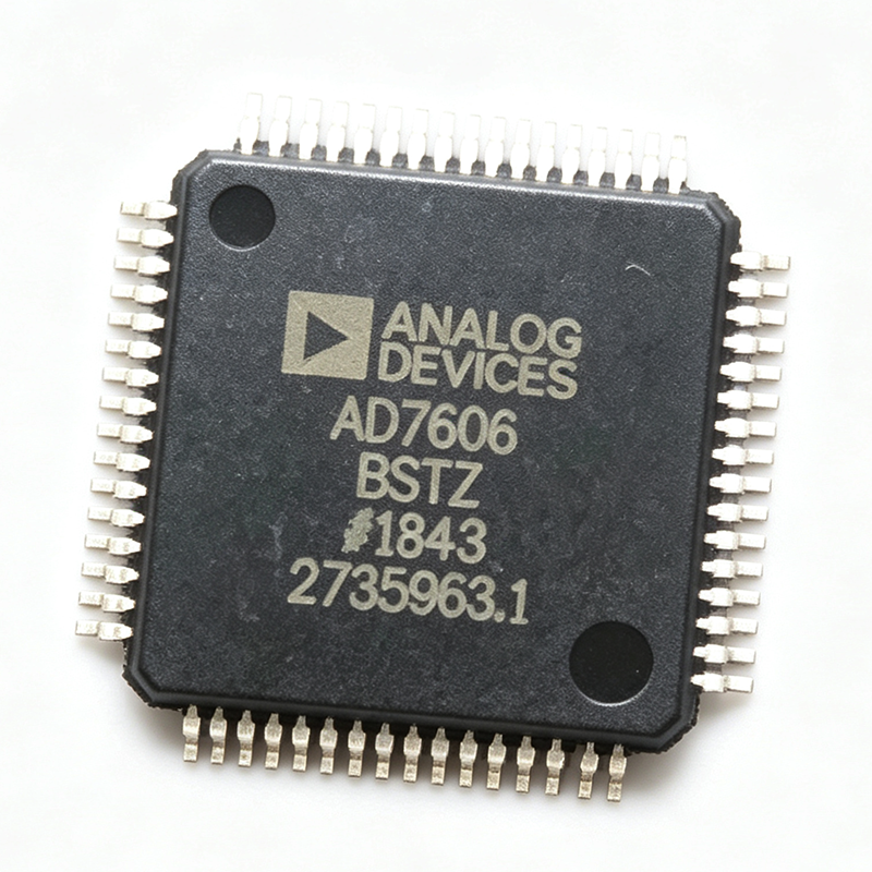
AD7606BSTZ - 16-Bit 8-Ch Simultaneous ADC | Analog Devices
The AD7606BSTZ is a 16-bit, 8-channel, simultaneous sampling analog-to-digital data acquisition system (DAS) from Analog Devices. It integrates analog input clamp protection, a second-order antialiasing filter, a track-and-hold amplifier, a 16-bit charge redistribution successive approximation ADC, a flexible digital filter, a 2.5V reference and reference buffer, and high-speed serial and parallel interfaces. The device operates from a single 5V supply and accepts bipolar input ranges of ±5V and ±10V, making it ideal for power-line monitoring and industrial data acquisition. A data acquisition system (DAS) is a complete signal chain that conditions, samples, and digitizes analog signals. The AD7606BSTZ belongs to the family of simultaneous sampling ADCs, which capture multiple channels at the same instant, preserving phase relationships critical for power metering and vibration analysis. It sits between analog sensors and a digital host processor, converting real-world signals into digital words for processing. Key features include 16-bit resolution, 200 kSPS throughput per channel, 8 simultaneous sampling channels, and a 64-lead LQFP package. The device offers a parallel, serial, SPI, QSPI, and MICROWIRE interface, providing flexibility for various host controllers. The integrated 2.5V reference and buffer eliminate the need for external reference components, simplifying design and reducing BOM cost. Technically, the AD7606BSTZ uses a successive approximation register (SAR) architecture with a charge redistribution DAC. The analog front end includes a second-order antialiasing filter with a cutoff frequency of 22 kHz, which attenuates out-of-band noise. The digital filter provides programmable oversampling ratios to further reduce noise. The device operates over the industrial temperature range of -40°C to +85°C and is available in a 10x10 mm LQFP package. Typical applications include power-line monitoring, protective relays, motor control, and multi-axis vibration analysis. The simultaneous sampling capability ensures accurate phase measurement between voltage and current channels, which is essential for power quality analysis. The high input impedance and integrated protection make it robust for harsh industrial environments. When designing with the AD7606BSTZ, ensure proper decoupling of the AVCC and DVCC supplies with 10 µF and 0.1 µF capacitors placed close to the pins. The REFIN/REFOUT pin can be driven by an external reference if higher accuracy is required, but the internal 2.5V reference is sufficient for most applications. The CONVST pins should be driven simultaneously to achieve true simultaneous sampling.

AD7606BSTZ-4 - 16-Bit 4-Ch Simultaneous Sampling ADC | Analog Devices
The AD7606BSTZ-4 from Analog Devices is a 16-bit, 4-channel simultaneous sampling analog-to-digital data acquisition system (DAS) in a 64-lead LQFP (10x10 mm) package. It operates from a single 5 V supply and accommodates true bipolar input signals of ±10 V and ±5 V while sampling at throughput rates up to 200 kSPS for all channels. The device integrates analog input clamp protection, a second-order antialiasing filter, a track-and-hold amplifier, a 16-bit charge redistribution successive approximation ADC, a flexible digital filter, a 2.5 V reference, and reference buffer. The AD7606BSTZ-4 supports multiple serial interface modes including DSP, MICROWIRE, QSPI, and SPI, as well as a parallel interface, making it versatile for various microcontroller and DSP connections. A data acquisition system (DAS) is a complete signal chain that conditions, samples, and converts analog signals into digital data for processing. The AD7606BSTZ-4 integrates the entire front-end, eliminating the need for external op-amps, filters, and references, which simplifies design and reduces board space. As a simultaneous sampling ADC, it captures all four channels at the same instant, which is critical for applications requiring phase-accurate measurements across multiple inputs, such as power monitoring and motor control. Key features include 1 MΩ analog input impedance regardless of sampling frequency, input clamp protection up to ±16.5 V, and a 3 dB cutoff frequency of 22 kHz for the antialiasing filter, providing 40 dB antialias rejection at 200 kSPS. The flexible digital filter is pin-driven, yielding improvements in SNR and reducing the 3 dB bandwidth. The device operates over the industrial temperature range of -40°C to +85°C and is RoHS compliant. The AD7606BSTZ-4 uses a charge redistribution successive approximation architecture, which offers excellent DC accuracy and low power consumption. The integrated 2.5 V reference and buffer ensure stable conversion results without external components. The device also features a flexible digital filter that can be configured via the oversampling pins to trade off throughput for noise performance, allowing designers to optimize SNR for their specific application. Typical applications include power line monitoring, protective relays, motor control, and industrial data acquisition systems. The simultaneous sampling capability and high input impedance make it ideal for measuring three-phase voltages and currents with phase accuracy. The wide input range and clamp protection ensure robust operation in harsh industrial environments. When designing with the AD7606BSTZ-4, ensure that the analog input signals are within the specified ±10 V or ±5 V ranges and that the supply decoupling is adequate. The device requires a clean 5 V supply and proper grounding to achieve the specified performance. The digital interface should be configured according to the host processor's requirements, and the oversampling pins should be set to achieve the desired balance between throughput and noise.
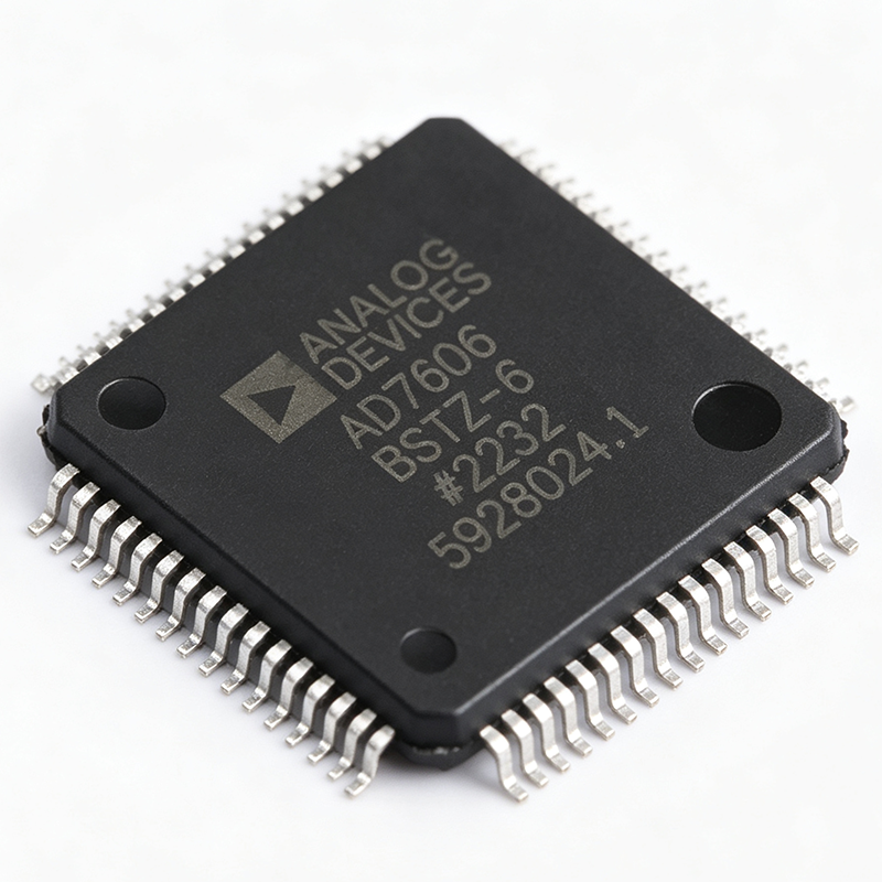
AD7606BSTZ-6RL - 16-Bit 6-Ch Simultaneous Sampling ADC | Analog Devices
The AD7606BSTZ-6RL is a 16-bit, simultaneous sampling, analog-to-digital data acquisition system (DAS) with six channels, manufactured by Analog Devices. It integrates analog input clamp protection, a second-order antialiasing filter, a track-and-hold amplifier, a 16-bit charge redistribution successive approximation ADC, a flexible digital filter, a 2.5 V reference and reference buffer, and high-speed serial and parallel interfaces. The device operates from a single 5 V supply and accepts bipolar input ranges of ±10 V, ±5 V, and ±2.5 V, making it ideal for industrial power-line monitoring, motor control, and data acquisition systems. A data acquisition system (DAS) is a complete signal chain that conditions, samples, and converts analog signals into digital data for processing. The AD7606BSTZ-6RL is a specific type of DAS that combines multiple analog front-end components into a single IC, reducing board space and design complexity. It belongs to the family of simultaneous sampling ADCs, which capture all channels at the same instant, preserving phase relationships between channels—critical for applications like three-phase power monitoring where phase accuracy is essential. Key features include a 200 kSPS throughput rate per channel, 16-bit resolution with no missing codes, and a flexible digital filter that can be configured for different output word rates. The device supports multiple interface options: parallel, serial, SPI, QSPI, MICROWIRE, and DSP-compatible serial interfaces, providing design flexibility. The integrated 2.5 V reference and buffer eliminate the need for external reference components, simplifying the BOM. The analog input clamp protection ensures robustness against overvoltage conditions up to ±16.5 V. Technically, the AD7606BSTZ-6RL uses a charge redistribution successive approximation architecture, which offers excellent linearity and low power consumption. The second-order antialiasing filter provides -80 dB attenuation at the Nyquist frequency, reducing the need for external filtering. The device operates over the industrial temperature range of -40°C to +85°C and is available in a 64-lead LQFP (10x10 mm) package, suitable for space-constrained designs. Typical applications include power line monitoring, protective relays, motor control, and multi-phase data acquisition systems. The simultaneous sampling capability ensures accurate phase measurement, while the high input impedance and integrated protection make it robust for harsh industrial environments. When designing with this device, ensure proper decoupling of the AVCC and DVCC supplies with 10 µF and 0.1 µF capacitors placed close to the pins. The REFIN/REFOUT pin can be overdriven with an external reference if higher accuracy is required, but the internal 2.5 V reference is sufficient for most applications.
AD7606BSTZ-RL - 16-Bit 8-Ch Simultaneous ADC | Analog Devices
The AD7606BSTZ-RL is a 16-bit, 8-channel, simultaneous sampling analog-to-digital data acquisition system (DAS) from Analog Devices. It integrates analog input clamp protection, a second-order antialiasing filter, a track-and-hold amplifier, a 16-bit charge redistribution successive approximation (SAR) ADC, a flexible digital filter, a 2.5 V reference and reference buffer, and high-speed serial and parallel interfaces. The device operates from a single 5 V supply and accepts bipolar input ranges of ±5 V and ±10 V, making it ideal for industrial power-line monitoring, motor control, and multi-phase energy measurement. A data acquisition system (DAS) is a complete signal chain that conditions, samples, and converts analog signals into digital data for processing. The AD7606 integrates the entire front-end, eliminating the need for external op-amps, references, and antialiasing filters, thereby reducing board space and design complexity. As a simultaneous sampling ADC, it captures all channels at the same instant, which is critical for applications requiring phase-accurate measurements across multiple inputs. Key features include a 200 kSPS throughput rate per channel, 16-bit resolution with no missing codes, and a 2.5 V internal reference with ±1% accuracy. The device offers both serial (SPI/QSPI/MICROWIRE) and parallel interfaces, and supports daisy-chaining for multiple devices. The flexible digital filter can be configured to improve noise performance, and the analog input clamp protects against overvoltage conditions up to ±16.5 V. The AD7606 uses a charge redistribution SAR architecture, which provides excellent linearity and low power consumption. The integrated antialiasing filter simplifies external filtering requirements, and the track-and-hold amplifier ensures accurate sampling of fast-changing signals. The device operates over the industrial temperature range of -40°C to +85°C and is available in a 64-lead LQFP package. Typical applications include power line monitoring, protective relays, motor control, and multi-phase energy measurement. The simultaneous sampling capability ensures accurate phase relationships between channels, which is essential for power quality analysis. The device is also suitable for vibration analysis and other multi-channel data acquisition systems. When designing with the AD7606, ensure that the analog input range is properly configured via the RANGE pin, and that the reference decoupling capacitor is placed close to the REFIN/REFOUT pin. The digital interface should be matched to the host processor's voltage level, and the AVCC and DVCC supplies should be decoupled with 0.1 µF and 10 µF capacitors.
AD7608BSTZ - 8-Channel 18-Bit Simultaneous Sampling ADC | Analog Devices
The AD7608BSTZ is a high-performance, 8-channel, 18-bit, bipolar, simultaneous sampling analog-to-digital data acquisition system (DAS) from Analog Devices. It integrates analog input clamp protection, a second-order antialiasing filter, a track-and-hold amplifier, an 18-bit charge redistribution successive approximation ADC, a flexible digital filter, a 2.5 V reference and reference buffer, and high-speed serial and parallel interfaces. The device operates from a single 5 V supply and accepts bipolar input ranges of ±10 V, ±5 V, and ±2.5 V, making it ideal for industrial power-line monitoring, motor control, and multi-phase energy measurement. A data acquisition system (DAS) is a complete signal chain that conditions, samples, and converts analog signals into digital data. The AD7608 integrates all essential analog front-end components, reducing external circuitry and design complexity. It belongs to the family of simultaneous sampling ADCs, which capture multiple channels at the same instant, preserving phase relationships critical for applications like three-phase power analysis and vibration monitoring. Key features include 18-bit resolution, a maximum sampling rate of 200 kSPS per channel, and simultaneous sampling across all eight channels. The device offers a flexible digital filter with programmable oversampling ratios, a 2.5 V internal reference with buffer, and both serial (SPI/DSP) and parallel interfaces. The input clamp protection and antialiasing filter simplify external signal conditioning, while the bipolar input ranges eliminate the need for level-shifting circuitry. The AD7608 uses a charge redistribution successive approximation architecture, providing excellent linearity and low noise. The integrated reference buffer ensures stable operation over temperature, and the flexible digital filter allows trade-offs between noise performance and output data rate. The device is available in a 64-lead LQFP package (10x10 mm), suitable for space-constrained industrial designs. Typical applications include power-line monitoring, protective relays, motor control, and multi-phase energy metering. The simultaneous sampling capability ensures accurate phase measurement, while the high resolution and bipolar inputs accommodate a wide range of sensor outputs. The device is also used in vibration analysis and instrumentation where multi-channel synchronization is essential. When designing with the AD7608, ensure proper decoupling of the AVCC and DVCC supplies, and place the reference decoupling capacitor close to the REFIN/REFOUT pin. The flexible digital filter can be configured to reduce noise, but it increases the settling time, so balance the oversampling ratio against the required throughput.
AD7609BSTZ - 18-Bit 8-Ch Simultaneous Sampling ADC | Analog Devices
The AD7609BSTZ is an 18-bit, 8-channel, true differential, simultaneous sampling analog-to-digital data acquisition system (DAS) from Analog Devices. It integrates analog input clamp protection, a second-order antialiasing filter, a track-and-hold amplifier, an 18-bit charge redistribution successive approximation ADC, a flexible digital filter, a 2.5 V reference and reference buffer, and high speed serial and parallel interfaces. The device operates from a single 5 V supply and supports a throughput rate of 200 kSPS, making it ideal for power line monitoring, motor control, and industrial data acquisition. A data acquisition system (DAS) is a complete signal chain that conditions, samples, and converts analog signals into digital data. The AD7609BSTZ belongs to the family of simultaneous sampling ADCs, which capture multiple channels at the same instant to preserve phase relationships between signals. This is critical in applications like three-phase power monitoring and multi-axis motor control, where timing skew between channels would introduce measurement errors. The DAS integrates the entire analog front end, reducing external component count and simplifying design. Key features include 18-bit resolution with no missing codes, 200 kSPS throughput on all channels, true differential inputs with a ±5 V or ±10 V range, and a 2.5 V internal reference with buffer. The device offers both serial (SPI/DSP) and parallel interfaces, and includes a digital filter for noise reduction. The input clamp protection tolerates voltages up to ±16.5 V, enhancing robustness in industrial environments. The AD7609BSTZ uses a charge redistribution successive approximation architecture, which provides excellent linearity and low power consumption. The integrated antialiasing filter simplifies external filtering requirements, and the track-and-hold amplifiers ensure accurate sampling of fast-changing signals. The device operates over the industrial temperature range of -40°C to +85°C and is available in a 64-lead LQFP (10x10 mm) package. Typical applications include power line monitoring, protective relays, motor control, and industrial data acquisition systems. The simultaneous sampling capability is essential for measuring three-phase voltages and currents with accurate phase alignment. The wide input range and robust protection make it suitable for harsh industrial environments. When designing with the AD7609BSTZ, ensure proper decoupling of the AVCC and DVCC supplies with 10 µF and 0.1 µF capacitors. The REFIN/REFOUT pin can be driven by an external reference for improved accuracy. The digital interface supports both serial and parallel modes, selectable via the PAR/SER/BYTE pin. For best performance, use a low-jitter conversion clock and minimize digital noise coupling to the analog inputs.
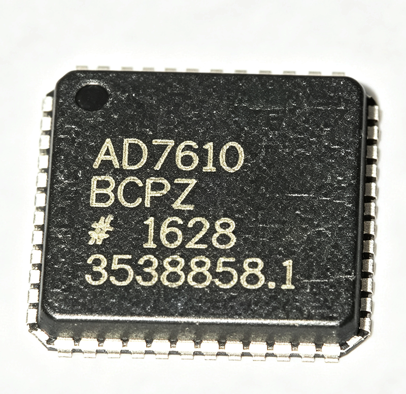
AD7610BCPZ - 16-Bit 250kSPS PulSAR ADC | Analog Devices
The AD7610BCPZ is a 16-bit, 250 kSPS successive approximation register (SAR) analog-to-digital converter (ADC) from Analog Devices, fabricated on the iCMOS high voltage process. It features a unipolar/bipolar programmable input range, allowing flexible configuration for various signal levels. The device operates from a 4.75V to 5.25V analog supply and is available in a 48-lead LFCSP-VQ (7x7) package, suitable for space-constrained industrial and instrumentation designs. A SAR ADC is a type of analog-to-digital converter that uses a binary search algorithm to convert an analog input into a digital output. It offers a good balance of speed, resolution, and power consumption, making it ideal for applications requiring high accuracy at moderate sampling rates. The AD7610 belongs to the PulSAR family, known for its high performance and ease of use, and is part of the broader data acquisition signal chain, which includes analog front-end conditioning, ADC conversion, and digital processing. Key features of the AD7610BCPZ include a 16-bit resolution with no missing codes, a maximum sampling rate of 250 kSPS, and a programmable input range that supports both unipolar (0V to 5V) and bipolar (±5V, ±10V) inputs. The device also offers a high-speed serial interface (SPI) for easy connection to microcontrollers and DSPs, and it includes an internal reference buffer, reducing external component count. The iCMOS process ensures low power dissipation and high voltage handling capability. The AD7610 uses a charge redistribution architecture with a capacitive DAC, providing excellent linearity and low noise. It features a track-and-hold amplifier that captures the input signal accurately, and the conversion result is output via a 16-bit serial word. The device supports both hardware and software configuration of the input range and operating mode, offering flexibility in system design. The LFCSP package includes an exposed pad for improved thermal performance, and the device operates over the industrial temperature range of -40°C to +85°C. Typical applications for the AD7610BCPZ include industrial process control, data acquisition systems, medical instrumentation, and test and measurement equipment. Its high resolution and programmable input range make it suitable for precision measurement of sensor signals, such as temperature, pressure, and strain. The device is also used in vibration analysis and power quality monitoring, where accurate and fast conversion is essential. When designing with the AD7610BCPZ, it is important to provide a clean analog supply and proper decoupling to achieve specified performance. The reference input should be bypassed with a low-ESR capacitor, and the digital interface should be isolated from noisy digital circuitry to minimize coupling. The exposed pad should be soldered to a ground plane for optimal thermal and electrical performance.
AD7610BCPZ-RL - 16-Bit 500kSPS SAR ADC | Analog Devices
The AD7610BCPZ-RL is a 16-bit charge redistribution successive approximation register (SAR) analog-to-digital converter (ADC) fabricated on Analog Devices' iCMOS high voltage process. It offers a maximum sampling rate of 500 kSPS and features a programmable input range supporting both unipolar and bipolar operation. The device is available in a 48-lead LFCSP-VQ (7x7 mm) package and is designed for high-performance data acquisition systems. An ADC (analog-to-digital converter) is an electronic component that converts continuous analog signals into discrete digital values. The AD7610 is a SAR ADC, which uses a binary search algorithm to determine the digital output, offering a good balance of speed, resolution, and power consumption. SAR ADCs are widely used in industrial, medical, and instrumentation applications where high accuracy and moderate sampling rates are required. Key features of the AD7610 include a 16-bit resolution, a maximum throughput of 500 kSPS, and a programmable input range that can be configured via hardware pins or a serial configuration port. The device operates from a single 5V analog supply and a 2.3V to 5.25V digital interface supply, making it compatible with a wide range of digital hosts. It also features a high-speed parallel and serial interface, allowing flexible connection to microcontrollers and DSPs. The AD7610 uses a charge redistribution architecture with an internal reference buffer, providing excellent linearity and low noise performance. The device includes an internal clock and can be configured for various operating modes, including normal, impulse, and fast modes, to optimize power consumption versus throughput. The iCMOS process enables high voltage operation while maintaining low power dissipation. Typical applications for the AD7610 include industrial process control, medical instrumentation, data acquisition systems, and automated test equipment. Its high resolution and programmable input range make it suitable for precision measurement applications where signal conditioning is required. When designing with the AD7610, it is important to provide adequate decoupling on the analog and digital supplies and to ensure a clean reference voltage for optimal performance. The device's input range should be configured to match the signal amplitude to maximize dynamic range.

AD7610BSTZ - 16-Bit 250kSPS SAR ADC | Analog Devices
The AD7610BSTZ is a 16-bit, 250 kSPS successive approximation register (SAR) analog-to-digital converter (ADC) from Analog Devices, fabricated on the iCMOS high voltage process. It features a unipolar/bipolar programmable input range, making it versatile for various data acquisition systems. The device is available in a 48-lead LQFP (7x7 mm) package and operates over the industrial temperature range. An ADC (analog-to-digital converter) is an electronic component that converts continuous analog signals into discrete digital numbers, enabling digital processing and storage. SAR ADCs use a binary search algorithm to approximate the input voltage, offering a good balance of speed, resolution, and power consumption. The AD7610 belongs to the PulSAR family, known for high accuracy and low power, and is part of the broader data converter hierarchy within mixed-signal ICs. Key features include a 16-bit resolution with no missing codes, a maximum throughput of 250 kSPS, and programmable input ranges of ±10 V, ±5 V, 0 to 10 V, and 0 to 5 V. It offers a parallel and serial interface, an internal reference, and a temperature range of -40°C to +85°C. The device also includes a busy indicator and a power-down mode for power-sensitive applications. The AD7610 uses a charge redistribution SAR architecture, which provides excellent linearity and low noise. The iCMOS process enables high voltage operation and reduces power consumption. The device includes an internal reference buffer and can operate with a 5 V analog supply and 2.3 V to 5.25 V digital supply, simplifying system design. Typical applications include industrial process control, data acquisition systems, medical instrumentation, and automated test equipment. The programmable input range allows direct interface to sensors with different output spans, reducing external signal conditioning. The high throughput and accuracy make it suitable for multi-channel multiplexed systems. When designing with the AD7610, ensure proper decoupling of the analog and digital supplies and a clean reference voltage. The input signal should be buffered to avoid charge injection errors. The parallel interface timing must be respected for reliable data transfer.

AD7610BSTZ-RL - 16-Bit 250kSPS PulSAR ADC | Analog Devices
The AD7610BSTZ-RL is a 16-bit, 250 kSPS successive approximation register (SAR) analog-to-digital converter (ADC) from Analog Devices, fabricated on the iCMOS high voltage process. It features programmable input ranges of ±10 V, ±5 V, 10 V, and 5 V, selectable via pins or a serial SPI-compatible port. The device operates from a 5 V analog supply and a 2.3 V to 5.25 V digital interface supply, with a typical power dissipation of 115 mW at 250 kSPS. It is available in a 48-lead LQFP (7x7 mm) package, with the -RL suffix indicating tape and reel packaging. A SAR ADC is a type of analog-to-digital converter that uses a binary search algorithm to convert an analog input into a digital output. It employs a comparator and a successive approximation register to iteratively narrow down the input voltage range, achieving high resolution and speed with low power consumption. SAR ADCs are widely used in data acquisition systems, industrial process control, and medical instrumentation where high accuracy and moderate sampling rates are required. Key features of the AD7610 include 16-bit resolution with no missing codes, a maximum throughput of 250 kSPS, and multiple programmable input ranges. The device offers a high-speed parallel interface and a serial SPI-compatible interface, providing flexibility in system integration. It also includes an internal reference buffer and supports external references, enabling precise voltage scaling. The iCMOS process ensures high voltage handling and low noise performance. The AD7610 architecture uses charge redistribution, which provides inherent sample-and-hold functionality and excellent linearity. The device includes a track-and-hold amplifier that captures the input signal, followed by a capacitive DAC that performs the successive approximation. This design achieves a typical signal-to-noise ratio (SNR) of 89 dB and a total harmonic distortion (THD) of -107 dB, making it suitable for high-precision measurement applications. Typical applications include industrial process control, data acquisition systems, medical instrumentation, and automated test equipment. The programmable input ranges allow direct interface with sensors and transducers without external scaling circuitry, simplifying design and reducing component count. The high input impedance and low power consumption make it ideal for battery-powered portable instruments. When designing with the AD7610, ensure that the analog input is properly buffered and that the reference voltage is stable and low-noise. The device requires a clean power supply with adequate decoupling to achieve optimal performance. The serial interface can be used to configure the input range and power-down modes, reducing power consumption in battery-operated systems.
AD7621ASTZ - 16-Bit 3 MSPS SAR ADC | Analog Devices
The AD7621ASTZ is a 16-bit, 3 MSPS, charge redistribution successive approximation register (SAR) analog-to-digital converter (ADC) from Analog Devices. It operates from a single 2.5 V power supply and features a fully differential input, an internal conversion clock, and an internal reference buffer. The device is available in a 48-lead LQFP (7x7 mm) package, making it suitable for space-constrained industrial and medical applications. An ADC (analog-to-digital converter) is an electronic component that converts continuous analog signals into discrete digital values. The AD7621ASTZ belongs to the SAR ADC family, which uses a binary search algorithm to approximate the input voltage. SAR ADCs are known for their high speed, low power consumption, and excellent accuracy, making them ideal for applications requiring precise measurements at moderate sampling rates. The AD7621ASTZ is part of the PulSAR series, which is recognized for its high performance and reliability. Key features of the AD7621ASTZ include 16-bit resolution with 2 LSB integral nonlinearity (INL), a maximum sampling rate of 3 MSPS, and a fully differential input range of ±VREF. The device operates from a single 2.5 V supply, with an analog supply range of 2.37 V to 2.63 V, and features a serial and parallel interface for flexible data transfer. The internal conversion clock eliminates the need for an external clock, simplifying system design. The AD7621ASTZ uses a charge redistribution architecture that provides excellent linearity and low noise. The device includes an internal reference buffer, which reduces external component count and improves performance. The fully differential input allows for common-mode rejection, making it suitable for applications with noisy environments. The device also features a power-down mode to reduce power consumption when not converting. Typical applications for the AD7621ASTZ include medical imaging, high-speed data acquisition, industrial process control, and instrumentation. Its high speed and accuracy make it ideal for applications such as digital X-ray, ultrasound, and vibration analysis. The device's small package and low power consumption enable portable and battery-powered designs. When designing with the AD7621ASTZ, it is important to provide a clean, low-noise power supply and a stable reference voltage. The analog input should be driven with a low-impedance source to maintain accuracy. Proper decoupling of the power supply pins and careful PCB layout are essential to achieve the specified performance.
AD7621ASTZ-RL7 - 16-Bit 3MSPS PulSAR ADC | Analog Devices
The AD7621ASTZ-RL7 is a 16-bit, 3 MSPS, charge redistribution successive approximation register (SAR) analog-to-digital converter (ADC) from Analog Devices. It operates from a single 2.5 V power supply and features a fully differential input. The device is available in a 48-lead LQFP (7x7 mm) package, suitable for high-speed data acquisition systems. An ADC is an electronic component that converts an analog voltage or current into a digital number proportional to the magnitude of the signal. The AD7621 is a SAR-type ADC, which uses a binary search algorithm to determine the digital output. SAR ADCs are known for their high speed, low power consumption, and ease of use, making them ideal for applications requiring high-resolution sampling at moderate speeds. The AD7621 sits in the hierarchy of data converters, specifically within the family of high-speed, high-resolution ADCs used in industrial, medical, and communication systems. Key features of the AD7621 include a throughput of 3 MSPS in wideband warp and warp modes, 2 MSPS in normal mode, and 1.25 MSPS in impulse mode. It has an internal 2.048 V reference and supports a differential input range of ±VREF (with VREF up to 2.5 V). The device offers excellent linearity with 2 LSB INL (integral nonlinearity) and operates from a single 2.5 V supply, minimizing power consumption. The AD7621 also includes an internal conversion clock and a high-speed 16-bit sampling ADC, simplifying system design. Technically, the AD7621 uses a charge redistribution architecture that samples the analog input onto a capacitor array. The internal reference and conversion clock reduce external component requirements. The device provides both parallel and serial data interfaces, offering flexibility in system integration. The fully differential input provides common-mode rejection, improving noise performance in noisy environments. Typical applications for the AD7621 include high-speed data acquisition, medical imaging, instrumentation, and communication systems. Its high throughput and resolution make it suitable for applications such as digital oscilloscopes, spectrum analyzers, and industrial process control. The device's low power consumption and small package enable compact, portable designs. When designing with the AD7621, ensure proper decoupling of the power supply and reference pins. Use a low-noise reference and adequate analog input drive circuitry to achieve specified performance. The differential input should be driven with a suitable amplifier to maintain signal integrity.