ADC/DAC
Products (181)

AD7794BRUZ - 24-Bit Sigma-Delta ADC, 6-Channel | Analog Devices
The AD7794BRUZ is a complete analog front end for high precision measurement applications from Analog Devices. It integrates a low noise, 24-bit sigma-delta (Σ-Δ) analog-to-digital converter (ADC) with six differential inputs, an on-chip low noise instrumentation amplifier (in-amp), and a precision low drift internal band gap reference. The device operates from a 2.7V to 5.25V power supply and is available in a 24-lead TSSOP package, making it suitable for space-constrained designs. A sigma-delta ADC is an oversampling converter that uses a modulator and digital filter to achieve high resolution and excellent noise performance. The AD7794BRUZ belongs to the family of precision analog-to-digital converters, which are essential in data acquisition systems where accurate conversion of small analog signals is required. Its on-chip in-amp allows direct interfacing of low amplitude signals, eliminating the need for external gain stages. Key features include a 24-bit resolution, six differential inputs, programmable gain amplifier (PGA) with gains of 1, 2, 4, 8, 16, 32, 64, and 128, and a low noise of 40 nV/√Hz. The device also offers programmable excitation current sources, burnout currents, and a bias voltage generator. It supports both internal and external references, with up to two external differential references. The AD7794BRUZ operates over a temperature range of -40°C to +105°C and is RoHS compliant. The AD7794BRUZ uses a Σ-Δ architecture with a digital filter that provides 50Hz/60Hz rejection, making it ideal for noisy industrial environments. The on-chip in-amp has a gain bandwidth product that allows direct connection of sensors such as thermocouples, RTDs, and strain gauges. The device communicates via a serial peripheral interface (SPI) and includes a temperature sensor for cold-junction compensation. Typical applications include process control, temperature measurement, pressure sensing, and weigh scales. The AD7794BRUZ is also used in portable instrumentation and battery-powered devices due to its low power consumption of 500 µA typical. Its high resolution and low noise make it suitable for precision data acquisition systems. When designing with the AD7794BRUZ, ensure proper decoupling of the AVDD and DVDD supplies and use a clean analog ground plane. The reference inputs should be bypassed with 0.1 µF capacitors. The SPI interface should be isolated if the ADC is used in noisy environments.
AD7795BRUZ - 16-Bit Sigma-Delta ADC, 6-Channel | Analog Devices
The AD7795BRUZ is a low power, low noise, complete analog front end for high precision measurement applications from Analog Devices. It integrates a 16-bit sigma-delta ADC with six differential inputs, an on-chip low noise instrumentation amplifier (in-amp), and a precision bandgap reference in a 24-lead TSSOP package. The device operates from a single 2.7V to 5.25V supply and achieves up to 470 SPS output data rate, making it suitable for a wide range of precision sensing and data acquisition systems. An analog-to-digital converter (ADC) is a device that converts continuous analog signals into discrete digital values. The AD7795BRUZ is a sigma-delta ADC, a type of ADC that uses oversampling and noise shaping to achieve high resolution and excellent noise performance. It belongs to the family of precision data converters, which are essential in applications requiring accurate measurement of physical quantities such as temperature, pressure, and strain. The on-chip in-amp allows direct interfacing of small amplitude signals, eliminating the need for external amplification stages. Key features of the AD7795BRUZ include a 16-bit resolution, six differential input channels, a programmable gain amplifier (PGA) with gains of 1, 2, 4, 8, 16, 32, 64, and 128, and a low noise performance of 23 effective bits at 16.7 Hz output rate. The device also features a low power consumption of 400 µA typical, with a power-down mode that reduces current to 1 µA max. It includes an internal band gap reference with low drift, and can accept up to two external differential references. The ADC communicates via a serial interface, compatible with SPI, and operates over a temperature range of -40°C to +105°C. The AD7795BRUZ is designed for high precision measurement applications, including temperature sensing with RTDs and thermocouples, pressure measurement, and weigh scales. Its low noise and high resolution make it ideal for bridge sensors and other low-level signal conditioning. The device is available in a 24-lead TSSOP package, which is compact and suitable for space-constrained designs. The package is RoHS compliant and lead-free. Typical applications include industrial process control, medical instrumentation, and portable battery-powered devices. The low power consumption and power-down mode extend battery life in portable applications. The on-chip in-amp and reference reduce external component count, simplifying design and improving reliability. When designing with the AD7795BRUZ, it is important to provide adequate decoupling on the AVDD and DVDD supplies, and to use a clean analog ground plane. The reference inputs should be bypassed with low ESR capacitors. The serial interface should be isolated from noisy digital circuitry to maintain the ADC's noise performance.

AD7796BRUZ - 16-Bit Sigma-Delta ADC for Bridge Sensors | Analog Devices
The AD7796BRUZ is a low power, 16-bit sigma-delta analog-to-digital converter (ADC) from Analog Devices, specifically designed for high precision bridge sensor applications such as weigh scales. It integrates a complete analog front end, including a programmable gain instrumentation amplifier with a fixed gain of 128, enabling direct interfacing of small amplitude signals from bridge sensors. The device operates from a 2.7V to 5.25V power supply and features a 16-bit resolution with a sigma-delta architecture, ensuring high accuracy and noise performance. The AD7796BRUZ is available in a 16-lead TSSOP package, making it suitable for space-constrained designs. An analog-to-digital converter (ADC) is a critical component in electronic systems that converts continuous analog signals into discrete digital values for processing by microcontrollers or digital signal processors. Sigma-delta ADCs, like the AD7796, use oversampling and noise shaping to achieve high resolution and excellent noise performance, making them ideal for precision measurement applications. The AD7796 belongs to the family of sigma-delta ADCs, which are widely used in industrial instrumentation, medical devices, and sensor interfaces where accuracy is paramount. Key features of the AD7796BRUZ include a fixed gain of 128, which eliminates the need for external amplification stages, and a low power consumption of typically 1.5 mA, making it suitable for battery-powered applications. The device also includes an on-chip temperature sensor, a reference voltage source, and a serial interface compatible with SPI, simplifying system integration. The ADC supports a data rate of up to 470 Hz, providing fast conversion for real-time monitoring. The AD7796BRUZ utilizes a sigma-delta modulator followed by a digital filter, achieving high resolution and low noise. The on-chip instrumentation amplifier with a gain of 128 allows direct connection to bridge sensors, reducing external component count and improving system reliability. The device also features a differential input, which helps reject common-mode noise, and a programmable gain amplifier that can be configured for various sensor outputs. Typical applications for the AD7796BRUZ include weigh scales, strain gauge measurements, pressure sensors, and other bridge-based sensing systems. Its high resolution and low noise make it ideal for precision industrial and medical instrumentation. The device is also suitable for portable devices due to its low power consumption. When designing with the AD7796BRUZ, it is important to ensure proper decoupling of the power supply and careful PCB layout to minimize noise. The reference voltage should be stable and low-noise to achieve optimal performance. Additionally, the SPI interface should be configured correctly to avoid communication errors.
AD7797BRUZ - 24-Bit Sigma-Delta ADC for Bridge Sensors | Analog Devices
The AD7797BRUZ is a low power, 24-bit sigma-delta analog-to-digital converter (ADC) from Analog Devices, specifically designed for high precision bridge sensor applications such as weigh scales. It integrates a complete analog front end including a programmable gain instrumentation amplifier with a fixed gain of 128, enabling direct interface to small amplitude signals from bridge sensors. The device operates from a 2.7V to 5.25V power supply and features a 16-pin TSSOP package, making it suitable for space-constrained designs. A sigma-delta ADC is a type of analog-to-digital converter that uses oversampling and noise shaping to achieve high resolution. It is part of the broader category of ADCs, which are essential components in data acquisition systems, converting analog signals into digital data for processing. The AD7797BRUZ is a complete analog front end, combining the ADC with an instrumentation amplifier and reference, simplifying the design of precision measurement systems. Key features include a 24-bit resolution, a fixed gain of 128, and a low power consumption of typically 500 µA. The device also includes a 2-wire serial interface (SPI) for communication, an internal reference, and a temperature sensor. The AD7797BRUZ is designed for bridge sensor applications, providing high accuracy and stability over temperature. The AD7797BRUZ uses a sigma-delta architecture with a digital filter, achieving high resolution and low noise. The on-chip instrumentation amplifier has a fixed gain of 128, allowing direct connection to bridge sensors without external amplification. The device also includes a burnout current source for sensor fault detection, enhancing system reliability. Typical applications include weigh scales, strain gauge measurements, pressure sensors, and other bridge-based transducers. The AD7797BRUZ is ideal for battery-powered portable instruments due to its low power consumption and small package size. When designing with the AD7797BRUZ, ensure proper decoupling of the power supply and reference pins. The SPI interface should be isolated from noisy digital lines to maintain accuracy. The device is available in a 16-lead TSSOP package, which is suitable for compact PCB layouts.
AD7798BRUZ - 16-Bit Sigma-Delta ADC, 3-Channel | Analog Devices
The AD7798BRUZ is a low-power, 16-bit Sigma-Delta analog-to-digital converter (ADC) from Analog Devices, featuring three differential input channels and an on-chip instrumentation amplifier (in-amp). It operates from a single 2.7V to 5.25V supply and is available in a 16-lead TSSOP package. The device integrates a precision reference, a low-side power switch, reference detect, programmable digital output pins, burnout currents, and an internal clock oscillator, making it a complete data acquisition solution for precision measurement applications. A Sigma-Delta ADC is a type of analog-to-digital converter that uses oversampling and noise shaping to achieve high resolution and excellent noise performance. It is ideal for low-frequency, high-precision applications such as sensor measurement, industrial process control, and instrumentation. The AD7798BRUZ belongs to the family of Sigma-Delta ADCs, which are part of the broader category of data converters, essential in bridging analog signals to digital processing systems. Key features of the AD7798BRUZ include a programmable output data rate from 4.17 Hz to 470 Hz, RMS noise as low as 1.5 µV (at 4.17 Hz), and a typical supply current of 400 µA, with a power-down mode consuming only 1 µA. The on-chip in-amp provides gain up to 128, allowing direct connection to low-level sensors such as thermocouples and strain gauges. The SPI-compatible serial interface simplifies communication with microcontrollers and DSPs. The device architecture includes a chopper-stabilized amplifier, a Sigma-Delta modulator, and a digital filter, ensuring high accuracy and low offset drift. The internal reference and clock reduce external component count, while the low-side power switch enables bridge sensor excitation. The AD7798BRUZ is specified for the industrial temperature range of -40°C to +105°C, making it suitable for harsh environments. Typical applications include temperature measurement with RTDs and thermocouples, pressure and strain gauge sensing, and battery monitoring. Its low power consumption and high resolution make it ideal for portable and battery-powered instruments. The device is also used in weigh scales and process control systems where precision is critical. When designing with the AD7798BRUZ, ensure proper decoupling of the AVDD and DVDD supplies with 0.1 µF and 10 µF capacitors, and place the reference decoupling capacitor close to the REFIN pins. The SPI interface should be isolated if the ADC is remote from the controller to avoid ground loops.
AD7799BRUZ - 24-Bit Sigma-Delta ADC with In-Amp | Analog Devices
The AD7799BRUZ is a low power, low noise, complete analog front end for high precision measurement applications from Analog Devices. It integrates a 24-bit Sigma-Delta ADC with three differential analog inputs and an on-chip instrumentation amplifier, all in a compact 16-lead TSSOP package. The device operates from a 2.7V to 5.25V supply and features a programmable output data rate from 4.17 Hz to 470 Hz, making it ideal for precision sensor and industrial measurement systems. A Sigma-Delta ADC is an analog-to-digital converter that uses oversampling and noise shaping to achieve high resolution, typically 16 to 24 bits, by trading speed for accuracy. It is the preferred choice for low-frequency, high-precision applications such as weigh scales, temperature sensors, and pressure transducers, where the signal bandwidth is narrow but the required resolution is high. The AD7799 belongs to the family of precision Sigma-Delta ADCs, which are essential building blocks in data acquisition systems, bridging the analog sensor world to the digital processing domain. Key features of the AD7799BRUZ include a low noise performance of 40 nV/√Hz, an on-chip low-side power switch, reference detect, programmable digital output pins, burnout currents, and an internal clock oscillator. The device also offers a programmable gain amplifier (PGA) with gains of 1, 2, 4, 8, 16, 32, 64, and 128, allowing direct connection to low-level sensor outputs. The output data rate is software-programmable, and the device supports both external and internal references, providing flexibility in system design. Technically, the AD7799 uses a third-order Sigma-Delta modulator followed by a digital filter, achieving excellent noise performance and linearity. The on-chip in-amp allows direct interface to bridge sensors and thermocouples without external signal conditioning. The device includes a SPI-compatible serial interface for configuration and data readout, and it operates over the industrial temperature range of -40°C to +105°C. The TSSOP-16 package is ideal for space-constrained designs, and the device is RoHS compliant. Typical applications include weigh scales, strain gauge transducers, temperature measurement with RTDs and thermocouples, pressure sensors, and general precision data acquisition. The low power consumption of 500 µA makes it suitable for battery-powered and portable instruments. The AD7799BRUZ is a production part from Analog Devices, with a 1ku list price starting from $6.41 as of 2026-08-22. When designing with the AD7799BRUZ, ensure proper decoupling of the AVDD and DVDD supplies with 0.1 µF and 10 µF capacitors, and place the reference decoupling capacitor close to the REFIN pins. The on-chip PGA allows direct sensor connection, but care must be taken to avoid exceeding the common-mode input range. The SPI interface should be isolated from noisy digital lines to maintain the high resolution performance.
AD7942BCPZ - 14-Bit 250kSPS PulSAR ADC | Analog Devices
The AD7942BCPZ is a 14-bit, charge redistribution, successive approximation (SAR) analog-to-digital converter (ADC) from Analog Devices, part of the PulSAR family. It operates from a single power supply, VDD, between 2.3 V and 5.5 V, and features a maximum throughput of 250 kSPS. The device includes an internal conversion clock, a pseudo-differential input, and an SPI-compatible serial interface that supports daisy-chaining multiple ADCs on a single 3-wire bus. The AD7942BCPZ is available in a 10-lead MSOP package (also offered in LFCSP), making it suitable for space-constrained designs. An ADC (analog-to-digital converter) is an electronic component that converts continuous analog signals into discrete digital values. The AD7942 is a SAR ADC, which uses a binary search algorithm through a charge redistribution capacitor array to achieve high-speed, high-resolution conversion with low power consumption. SAR ADCs are widely used in data acquisition systems, industrial process control, and medical instrumentation where a balance of speed, resolution, and power efficiency is required. The AD7942 belongs to the PulSAR family, known for its no missing codes guarantee and excellent linearity. Key features of the AD7942BCPZ include 14-bit resolution with no missing codes, a maximum sampling rate of 250 kSPS, and a pseudo-differential input that rejects common-mode noise. The reference voltage (VREF) is applied externally and can be set up to the supply voltage, allowing flexible full-scale range selection. The device's power consumption scales linearly with throughput, making it ideal for battery-powered applications. The SPI interface includes an SDI input for daisy-chaining and an optional busy indicator, simplifying multi-channel systems. Technically, the AD7942 uses a charge redistribution architecture with an internal capacitor array, achieving excellent INL and DNL performance. The device operates over a temperature range of -40°C to +125°C, ensuring reliability in harsh environments. The MSOP-10 package has a thermal resistance of approximately 150°C/W, and the device is RoHS compliant. The external reference allows the user to optimize the full-scale range for specific applications, and the power dissipation is typically 4.5 mW at 250 kSPS with a 5V supply. Typical applications include battery-powered data acquisition systems, portable medical devices, industrial process control, and instrumentation. The AD7942's low power and high speed make it suitable for multi-channel systems where multiple ADCs are daisy-chained. The pseudo-differential input rejects common-mode noise, improving signal integrity in noisy industrial environments. When designing with the AD7942, ensure that the reference voltage is stable and properly decoupled, as it directly affects conversion accuracy. The SPI interface should be kept short to minimize parasitic capacitance, and the analog input should be driven by a low-impedance source to avoid sampling errors.
AD7944BCPZ - 14-Bit 2.5 MSPS PulSAR ADC | Analog Devices
The AD7944BCPZ is a 14-bit, 2.5 MSPS successive approximation register (SAR) analog-to-digital converter (ADC) from Analog Devices, part of the PulSAR family. It operates from a single 2.5 V supply and features a separate VIO supply for digital interface compatibility with 1.8 V, 2.5 V, and 2.7 V logic. The device is available in a 20-lead LFCSP (4x4 mm) package and is specified for operation from -40°C to +85°C. A SAR ADC is a type of analog-to-digital converter that uses a binary search algorithm to convert an analog input into a digital output. It typically offers high speed and low power consumption, making it suitable for applications such as data acquisition, industrial process control, and medical instrumentation. The AD7944 is a high-performance member of this family, providing 14-bit resolution at 2.5 MSPS while dissipating only 15.5 mW, which is ideal for power-sensitive portable and battery-powered systems. Key features of the AD7944 include a 14-bit resolution, 2.5 MSPS throughput, and a serial interface that is compatible with 1.8 V, 2.5 V, and 2.7 V supplies via the separate VIO supply. The device also offers a pseudo-differential input, an internal reference buffer, and a power-down mode to reduce power consumption when not converting. The LFCSP package provides a compact footprint for space-constrained designs. Technically, the AD7944 uses a charge redistribution SAR architecture with a capacitive DAC, achieving excellent linearity and low noise. The device includes an internal reference buffer that allows the use of an external reference, and it supports both SPI and daisy-chain modes for easy integration with microcontrollers and DSPs. The pseudo-differential input simplifies signal conditioning while maintaining good common-mode rejection. Typical applications for the AD7944 include high-speed data acquisition systems, industrial process control, medical imaging, and portable instrumentation. Its combination of speed, resolution, and low power makes it suitable for battery-powered devices where power efficiency is critical. The device is also used in communication systems for digitizing analog signals with high accuracy. When designing with the AD7944, ensure that the reference voltage is stable and well-decoupled, as it directly affects conversion accuracy. The VIO supply should be matched to the host interface logic level to avoid signal integrity issues. Proper PCB layout with separate analog and digital ground planes is recommended to minimize noise coupling.
AD7946BCPZ - 14-Bit 500kSPS PulSAR ADC | Analog Devices
The AD7946BCPZ is a 14-bit, charge redistribution, successive approximation analog-to-digital converter (ADC) from Analog Devices, operating from a single 5 V power supply (VDD). It achieves a throughput of 500 kSPS in Warp mode, 450 kSPS in Normal mode, and 380 kSPS in Impulse mode, making it suitable for high-speed data acquisition systems. The device is available in a 10-lead LFCSP (3 mm x 3 mm) package, offering a compact solution for space-constrained designs. An ADC (analog-to-digital converter) is an electronic component that converts continuous analog signals into discrete digital values, enabling digital processing of real-world signals. The AD7946 is a successive approximation register (SAR) ADC, which uses a charge redistribution architecture to achieve high accuracy and speed with low power consumption. SAR ADCs are widely used in applications requiring a balance of resolution, speed, and power efficiency, such as industrial process control, medical instrumentation, and portable devices. Key features of the AD7946 include 14-bit resolution with no missing codes, integral nonlinearity (INL) of 0.4 LSB typical and 1 LSB maximum, and differential nonlinearity (DNL) of 0.25 LSB typical and 0.7 LSB maximum. The device operates over an industrial temperature range of -40°C to +85°C and features a pseudo-differential analog input with an input voltage range of -0.5 V to 5.8 V. The AD7946 also includes a 1-pole low-pass filter on the analog input, which helps to reduce noise from the driving amplifier. The AD7946 uses a charge redistribution architecture with an internal sample-and-hold circuit, providing excellent AC and DC performance. The device supports multiple power-down modes, including Warp, Normal, and Impulse, allowing designers to optimize power consumption versus throughput. The SPI-compatible serial interface enables easy connection to microcontrollers and DSPs, and the device is fully specified for operation from a single 5 V supply. Typical applications for the AD7946 include high-speed data acquisition, industrial process control, medical instrumentation, and portable battery-powered devices. Its low power consumption and small package make it ideal for portable and space-constrained applications, while its high accuracy and speed suit demanding industrial and medical systems. When designing with the AD7946, ensure that the analog input is driven by a low-impedance source and that adequate decoupling is provided on the VDD pin. The device's noise performance is excellent, allowing the use of a noisier amplifier to meet system noise specifications, as the internal filter attenuates high-frequency noise.
AD7980ACPZ-RL7 - 16-Bit 1 MSPS SAR ADC | Analog Devices
The AD7980ACPZ-RL7 is a 16-bit, successive approximation register (SAR) analog-to-digital converter (ADC) from Analog Devices, offering a maximum sampling rate of 1 MSPS. It operates from a single 2.5 V supply (VDD) and features a versatile serial interface compatible with SPI, QSPI, MICROWIRE, and DSP protocols. The device is housed in a compact 10-lead LFCSP-WD (3x3 mm) package, ideal for space-constrained applications. An ADC (analog-to-digital converter) is an electronic component that converts continuous analog signals into discrete digital values, enabling digital processing of real-world signals. SAR ADCs use a binary search algorithm to approximate the input voltage, balancing speed and resolution. The AD7980 belongs to the PulSAR family, known for low power consumption and high accuracy, making it suitable for battery-powered and precision measurement systems. Key features include 16-bit resolution with no missing codes, a throughput of 1 MSPS, and low power dissipation that scales linearly with throughput. The reference voltage (REF) is applied externally and can be set independently of VDD, providing flexibility in system design. The device also supports daisy-chaining multiple ADCs on a single 3-wire bus via the SDI input, simplifying multi-channel data acquisition. The AD7980 uses a charge redistribution architecture with a capacitive DAC, achieving excellent linearity with INL of ±0.6 LSB typical and ±1.25 LSB maximum. Its SINAD performance is specified in the datasheet, ensuring high signal integrity for precision applications. The device operates over a wide temperature range and is available in both MSOP and LFCSP packages, with the LFCSP variant offering a smaller footprint. Typical applications include battery-powered instruments, data acquisition systems, medical devices, and industrial process control. The low power consumption and small package make it ideal for portable and embedded designs. The SPI-compatible interface allows easy integration with microcontrollers and DSPs. When designing with the AD7980, ensure a clean, low-impedance reference voltage and adequate decoupling on VDD and REF pins. The CNV pin initiates conversions on its rising edge, and the busy indicator can be used to synchronize data reads. Proper PCB layout with short analog input traces minimizes noise and maintains accuracy.
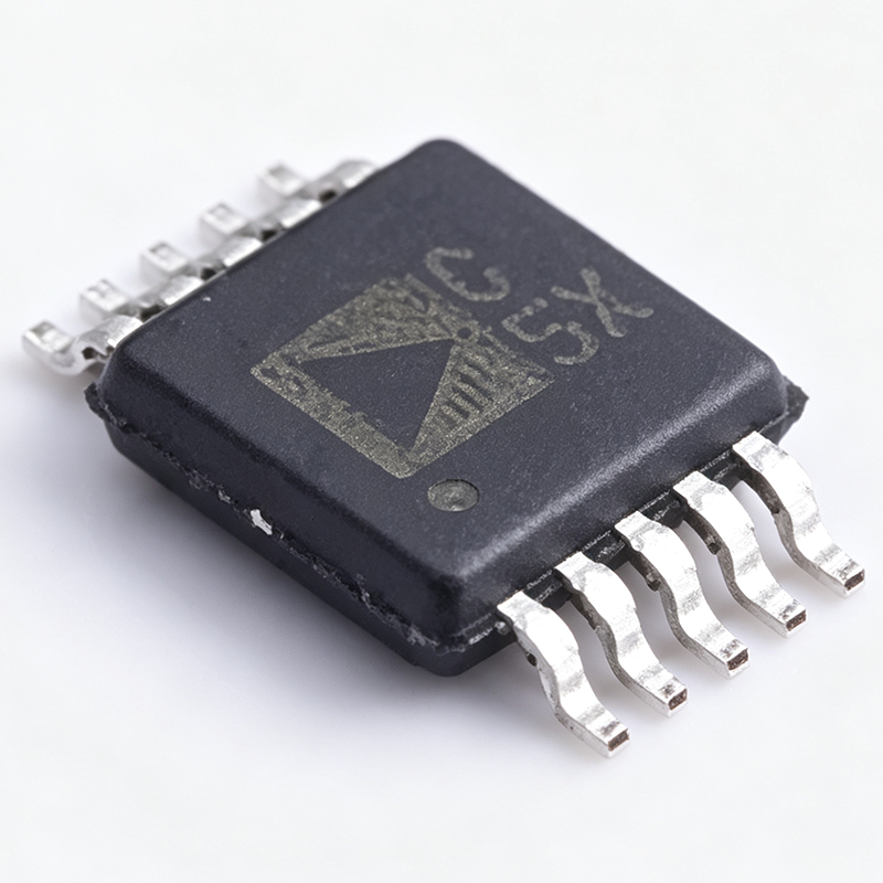
AD7980ARMZ - 16-Bit 1 MSPS PulSAR ADC | Analog Devices
The AD7980ARMZ is a 16-bit, 1 MSPS successive approximation register (SAR) analog-to-digital converter (ADC) from Analog Devices, housed in a 10-lead MSOP package. It operates from a single 2.5 V supply and features a pseudo-differential input, an SPI-compatible serial interface, and a throughput that scales linearly with power consumption. The device is pin-for-pin compatible with the 18-bit AD7982, offering a straightforward upgrade path for higher resolution. An ADC (analog-to-digital converter) is an electronic component that converts continuous analog signals into discrete digital numbers, enabling digital systems to process real-world signals. SAR ADCs use a successive approximation register to perform binary search across the reference voltage, achieving high speed and moderate resolution with low power. The AD7980 belongs to the PulSAR family, known for excellent AC and DC performance, and is widely used in precision data acquisition systems. Key features include a 16-bit resolution with no missing codes, a maximum sampling rate of 1 MSPS, and a typical signal-to-noise ratio (SNR) of 91.5 dB. The device supports an external reference voltage from 2.4 V to 5.1 V, allowing flexibility in system design. Its SPI-compatible interface supports daisy-chaining multiple ADCs on a single 3-wire bus and provides an optional busy indicator, simplifying multi-channel systems. The AD7980 uses a charge redistribution SAR architecture with a precision comparator and internal clock, achieving high accuracy without external components. The device operates over a temperature range of -40°C to +125°C and is available in both MSOP and LFCSP packages. Its power dissipation is only 7 mW at 1 MSPS, scaling linearly with throughput, making it ideal for battery-powered and portable applications. Typical applications include medical instrumentation, high-speed data acquisition, industrial process control, and battery-powered systems. The device's low power and small footprint make it suitable for space-constrained designs. When designing with the AD7980, ensure a clean, low-impedance reference source and adequate decoupling on the VDD and REF pins to achieve optimal performance.
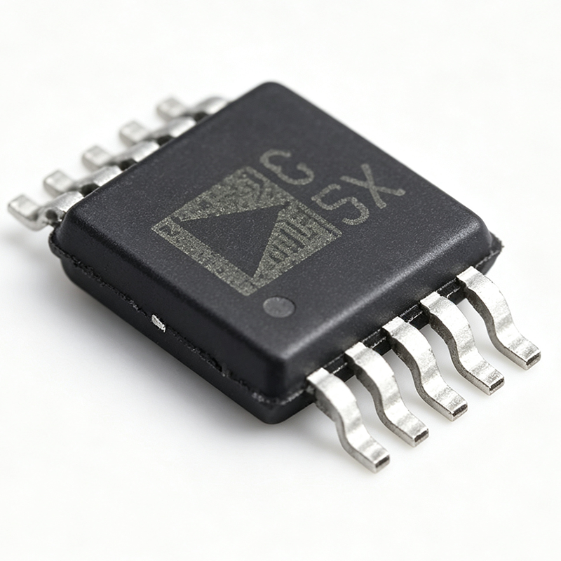
AD7980ARMZRL7 - 16-Bit 1 MSPS PulSAR ADC | Analog Devices
The AD7980ARMZRL7 is a 16-bit, 1 MSPS successive approximation register (SAR) analog-to-digital converter (ADC) from Analog Devices, housed in a 10-lead MSOP package. It operates from a single 2.5 V supply and features a pseudo-differential input, an SPI-compatible serial interface, and a throughput that scales linearly with power consumption. The device is pin-for-pin compatible with the 18-bit AD7982, offering a straightforward upgrade path for higher resolution. An ADC (analog-to-digital converter) is an electronic component that converts a continuous analog voltage into a discrete digital representation. The AD7980 is a SAR-type ADC, which uses a binary search algorithm to determine the digital output, offering a good balance of speed, resolution, and power consumption. SAR ADCs are widely used in data acquisition systems, industrial process control, and medical instrumentation where high accuracy and low latency are required. Key features of the AD7980 include a 1 MSPS throughput rate, 16-bit resolution with a maximum integral nonlinearity (INL) of ±2.5 LSB, and a signal-to-noise ratio (SNR) of 91.5 dB at 1 kHz input frequency. The device operates from a 2.5 V supply and consumes only 7 mW at 1 MSPS, with power scaling linearly with throughput. The reference voltage is applied externally and can be set independently of the supply voltage, providing flexibility in system design. The AD7980 uses a charge redistribution SAR architecture with a precision comparator and an internal capacitive DAC. It features a pseudo-differential input that rejects common-mode noise, and the SPI interface supports daisy-chaining multiple ADCs on a single 3-wire bus using the SDI input. The device also provides an optional busy indicator for synchronization. Typical applications include battery-powered instrumentation, portable medical devices, data acquisition systems, and industrial process control. The low power consumption and small package make it ideal for space-constrained designs. The external reference allows the input range to be optimized for the specific sensor or signal conditioning circuit. When designing with the AD7980, ensure that the reference voltage is stable and well-decoupled, as it directly affects conversion accuracy. The analog input should be driven by a low-impedance source to avoid sampling errors, and the SPI bus should be kept short to minimize noise.
AD7980BCPZ-RL7 - 16-Bit 1 MSPS PulSAR ADC | Analog Devices
The AD7980BCPZ-RL7 is a 16-bit, successive approximation (SAR) analog-to-digital converter (ADC) from Analog Devices, offering a throughput of 1 MSPS. It operates from a single power supply, VDD, and features a versatile serial interface port. The device is housed in a compact 10-lead LFCSP-WD (3x3 mm) package, making it suitable for space-constrained applications. An ADC (Analog-to-Digital Converter) is an electronic component that converts continuous analog signals into discrete digital values. The AD7980 belongs to the PulSAR family of SAR ADCs, which are known for their high precision, low power, and fast sampling rates. SAR ADCs are widely used in data acquisition systems, industrial process control, medical instrumentation, and portable devices where accuracy and speed are critical. Key features of the AD7980 include 16-bit resolution with no missing codes, a maximum INL of ±1.25 LSB, and a SINAD of [DATA_NEEDED: SINAD value] dB at 10 kHz. The device supports a pseudo-differential analog input range from 0 V to VREF, with VREF applied externally and independent of VDD. Power dissipation scales linearly with throughput, making it efficient for low-speed applications. The AD7980 uses a charge redistribution SAR architecture, which provides excellent linearity and low noise. The SPI-compatible serial interface supports daisy-chaining multiple ADCs on a single 3-wire bus and includes an optional busy indicator. The device can interface with any 1.8 V to 5 V digital logic family, offering flexibility in system design. Typical applications include battery-powered instruments, data acquisition systems, industrial process control, and medical devices. The low power dissipation and small package make it ideal for portable and high-density designs. When designing with the AD7980, ensure that the reference voltage (REF) is stable and well-decoupled, as it directly affects conversion accuracy. The analog input should be driven by a low-impedance source to maintain the specified performance.
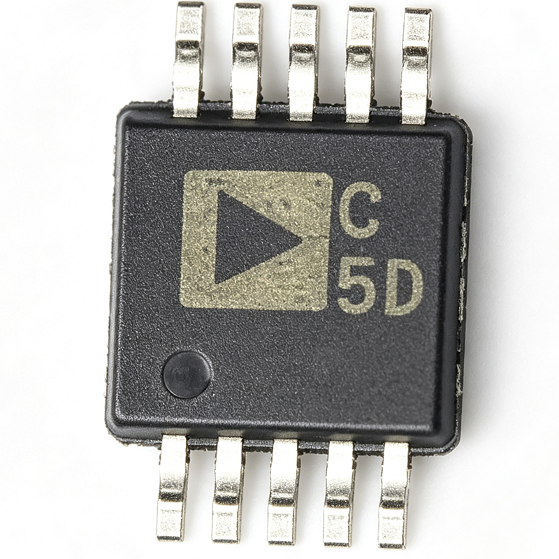
AD7980BRMZ - 16-Bit 1 MSPS PulSAR ADC | Analog Devices
The Analog Devices AD7980BRMZ is a 16-bit, 1 MSPS successive approximation register (SAR) analog-to-digital converter housed in a compact 10-lead MSOP package. It operates from a single VDD supply and contains a low-power, high-speed 16-bit sampling ADC with a versatile SPI-compatible serial interface. The pseudo-differential analog input range extends from 0 V to VREF, where VREF is applied externally and can be set independent of VDD. According to the AD7980 datasheet (Rev. G), the part is pin-for-pin compatible with the 18-bit AD7982. A SAR ADC is an analog-to-digital converter that determines the output code using a binary-search algorithm, comparing the held input against a DAC output one bit at a time. SAR ADCs balance resolution, speed, power, and small size, making them a common choice in precision data acquisition systems. Within the converter hierarchy, the AD7980 is a PulSAR ADC, a proprietary Analog Devices architecture optimized for low power and high accuracy. It sits in the broader signal-chain hierarchy of sensor → signal conditioning → ADC → digital host. Key features include 16-bit resolution with no missing codes, maximum INL of ±1.25 LSB, and a throughput of 1 MSPS. The device supports a pseudo-differential input for common-mode noise rejection, an external reference for flexible full-scale range selection, and a 3-wire SPI interface with daisy-chain capability and an optional BUSY indicator. The digital interface is compatible with 1.8 V to 5 V logic families, easing connection to a wide range of microcontrollers and FPGAs. Architecturally, the AD7980 uses an internal capacitor DAC and low-power comparator to achieve fast conversion while maintaining excellent linearity. Power dissipation scales linearly with throughput, which is advantageous in battery-powered and duty-cycled systems. The small 10-MSOP package and exposed pad provide space savings and flexible layout options for dense printed-circuit boards. Typical applications include industrial control, medical instrumentation, automated test equipment, precision sensor signal chains, and PLC analog input modules. The combination of 16-bit resolution, 1 MSPS speed, low power, and an SPI interface makes it suitable for multichannel systems where small board area is required. Designers should provide a low-impedance reference source, a driver amplifier with adequate settling time, and careful decoupling on VDD and VIO for best performance.
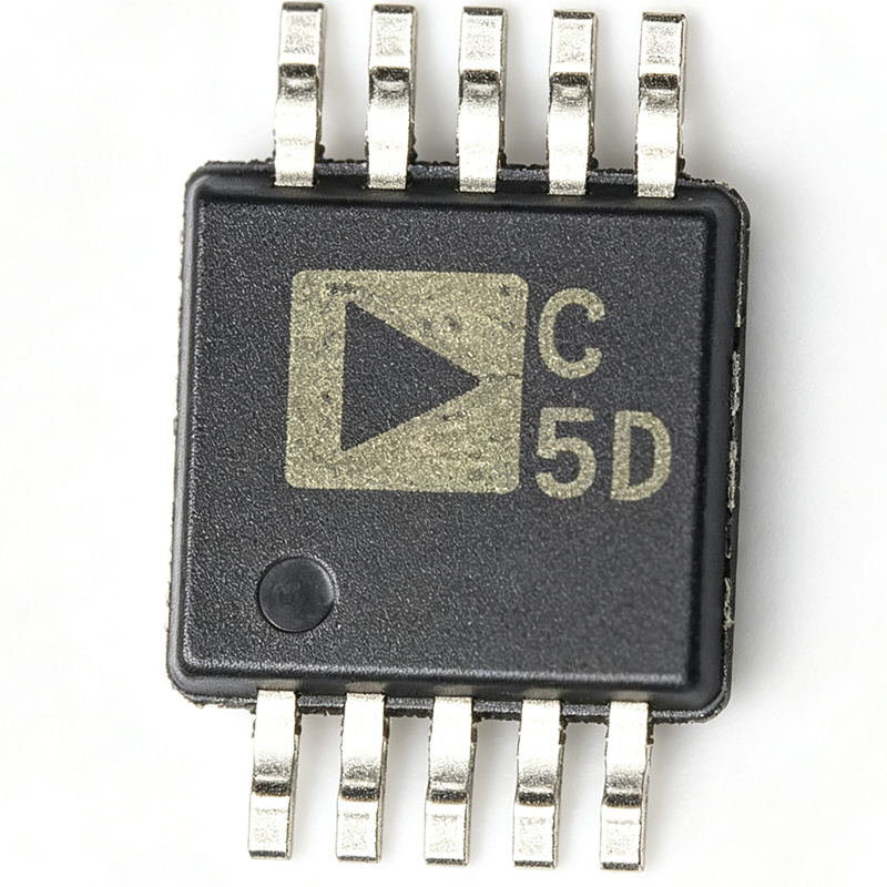
AD7980BRMZRL7 - 16-Bit 1 MSPS SAR ADC | Analog Devices
The AD7980BRMZRL7 is a 16-bit, 1 MSPS successive approximation register (SAR) analog-to-digital converter (ADC) from Analog Devices, housed in a 10-lead MSOP package. It operates from a single power supply, VDD, and features a low-power, high-speed 16-bit sampling ADC with a versatile serial interface port. The device is pin-for-pin compatible with the 18-bit AD7982, offering a straightforward upgrade path for higher resolution. A SAR ADC is a type of analog-to-digital converter that uses a binary search algorithm to convert an analog input into a digital output. It is known for its high speed, low power consumption, and excellent accuracy, making it ideal for applications such as data acquisition systems, industrial process control, and medical instrumentation. The AD7980 belongs to the PulSAR family of ADCs, which are renowned for their high performance and ease of use. Key features of the AD7980BRMZRL7 include a 16-bit resolution, a maximum sampling rate of 1 MSPS, and a pseudo-differential input. The reference voltage, REF, is applied externally and can be set independently of the supply voltage, VDD. Its power consumption scales linearly with throughput, making it energy-efficient for battery-powered applications. The SPI-compatible serial interface supports daisy-chaining multiple ADCs on a single 3-wire bus and provides an optional busy indicator. The AD7980 uses a charge redistribution SAR architecture, which provides excellent linearity and low noise. It operates from a 2.5 V to 5.5 V supply, and the digital interface can be connected to any 1.8 V to 5 V logic family. The device is available in both MSOP and LFCSP packages, offering flexibility in board design. The MSOP package is particularly suited for space-constrained applications. Typical applications include high-speed data acquisition, industrial automation, medical imaging, and portable instrumentation. The AD7980's low power consumption and high speed make it ideal for battery-operated devices that require accurate analog-to-digital conversion. Its small footprint and SPI interface simplify integration into existing digital systems. When designing with the AD7980, ensure that the reference voltage is stable and well-decoupled to achieve optimal performance. The analog input should be driven by a low-impedance source to minimize sampling errors. Proper PCB layout, including a solid ground plane and short traces, is essential for maintaining signal integrity.
AD7982BCPZ - 18-Bit 1 MSPS PulSAR ADC | Analog Devices
The AD7982BCPZ is an 18-bit, successive approximation register (SAR) analog-to-digital converter (ADC) from Analog Devices, offering a maximum throughput of 1 MSPS. It operates from a single 2.5 V supply (VDD) and features a separate VIO supply for digital interface compatibility with 1.8 V, 2.5 V, 3 V, or 5 V logic. The device is available in a 10-lead LFCSP-WD (3x3 mm) package, specified for operation from -40°C to +85°C. A SAR ADC is a type of analog-to-digital converter that uses a binary search algorithm to convert an analog input into a digital output. It typically offers high resolution, low power consumption, and fast conversion times, making it suitable for applications requiring precise measurements with moderate sampling rates. SAR ADCs are widely used in data acquisition systems, industrial process control, medical instrumentation, and portable devices. Key features of the AD7982 include 18-bit resolution with no missing codes, a throughput of 1 MSPS, and low power dissipation. At 1 MSPS, the power consumption is typically 7.5 mW, while at 10 kSPS it drops to 75 µW, making it ideal for battery-powered applications. The device achieves an integral nonlinearity (INL) of ±1 LSB typical and ±2 LSB maximum, and a dynamic range of 99 dB. It also features a versatile serial interface port that is compatible with SPI, QSPI, MICROWIRE, and DSP interfaces. The AD7982 uses a low-power, high-speed 18-bit sampling ADC architecture with a capacitive DAC and a precision comparator. The device includes an internal reference buffer and supports both external and internal reference options. The serial interface provides a daisy-chain mode for multiple ADC configurations, simplifying system design. The LFCSP package offers excellent thermal performance and a compact footprint for space-constrained designs. Typical applications include high-speed data acquisition, industrial process control, medical imaging, and portable instrumentation. The low power consumption and high resolution make it suitable for battery-powered devices, while the high throughput supports real-time monitoring systems. The device is also used in vibration analysis, motor control, and other precision measurement applications. When designing with the AD7982, ensure proper decoupling of the VDD and VIO supplies with 100 nF and 10 µF capacitors placed close to the pins. The reference input should be bypassed with a 10 µF capacitor to maintain stability. The serial clock (SCK) frequency should not exceed 50 MHz to ensure reliable data transfer. The device supports power-down modes to reduce power consumption further when not converting.
AD7984BCPZ - 18-Bit 1.33 MSPS SAR ADC | Analog Devices
The AD7984BCPZ is an 18-bit, 1.33 MSPS successive approximation register (SAR) analog-to-digital converter (ADC) from Analog Devices, part of the PulSAR family. It operates from a single 2.5 V supply and dissipates only 10.5 mW at full throughput, making it ideal for power-sensitive precision data acquisition systems. The device is available in a 10-lead LFCSP-WD (3x3 mm) package, offering a compact footprint for space-constrained designs. A SAR ADC is a type of analog-to-digital converter that uses a binary search algorithm to convert an analog input into a digital code. It employs a comparator and a digital-to-analog converter (DAC) to successively approximate the input voltage, achieving high resolution and speed with low power consumption. SAR ADCs are widely used in applications requiring high precision and moderate sampling rates, such as industrial process control, medical instrumentation, and scientific analysis. Key features of the AD7984BCPZ include 18-bit resolution with no missing codes, a true differential analog input range of ±VREF with VREF between 5.0 V, and an INL of ±2.25 LSB maximum. It offers a dynamic range of 99.7 dB typical and a signal-to-noise ratio (SNR) of 99 dB typical. The device features an SPI-compatible serial interface that supports daisy-chaining multiple ADCs on a single 3-wire bus and provides an optional busy indicator. The reference voltage is applied externally and can be set independent of the supply voltage. The AD7984BCPZ is pin-for-pin compatible with the 18-bit AD7982, allowing easy upgrades or substitutions in existing designs. It can interface with any 1.8 V to 5 V digital logic family, providing flexibility in mixed-voltage systems. The device operates over a temperature range of -40°C to +125°C, making it suitable for harsh industrial environments. Typical applications include high-speed data acquisition, medical imaging, spectroscopy, and vibration analysis. Its low power dissipation and high accuracy make it particularly well-suited for battery-powered portable instruments and remote sensing nodes. When designing with the AD7984BCPZ, ensure a clean, low-impedance reference voltage source and adequate decoupling on the VDD and REF pins. The SPI interface should be kept short to minimize noise, and the analog input should be driven by a low-impedance source to maintain accuracy.
AD7986BCPZ - 18-Bit 2 MSPS SAR ADC | Analog Devices
The AD7986BCPZ is an 18-bit, 2 MSPS successive approximation register (SAR) analog-to-digital converter (ADC) from Analog Devices, packaged in a 20-lead LFCSP (4x4 mm). It operates from a single 2.5 V supply and features a separate VIO supply for digital interface compatibility with 1.8 V, 2.5 V, and 2.7 V logic. The device consumes only 15 mW at 2 MSPS, making it ideal for high-speed, low-power data acquisition systems. An ADC (analog-to-digital converter) is an electronic component that converts continuous analog signals into discrete digital numbers, enabling digital processing and storage. SAR ADCs use a binary search algorithm to determine the digital output, offering a good balance of speed, resolution, and power consumption. The AD7986 belongs to the PulSAR family, known for high accuracy and low noise, and is used in applications such as medical imaging, industrial process control, and scientific instrumentation. Key features include a 2 MSPS throughput, 18-bit resolution, and a typical signal-to-noise ratio (SNR) of 98 dB. The device supports both SPI and daisy-chain serial interfaces, allowing multiple ADCs to be connected to a single bus. It also includes a busy indicator and a conversion result readback feature. The LFCSP package provides excellent thermal performance and a small footprint for space-constrained designs. The AD7986 uses a charge redistribution architecture with an internal reference buffer, achieving high linearity and low drift. The device operates over the industrial temperature range of -40°C to +85°C. Its low power dissipation and high speed make it suitable for portable and battery-powered instruments where power efficiency is critical. Typical applications include high-speed data acquisition, medical imaging (e.g., ultrasound), industrial automation, and test and measurement equipment. The device's high SNR and low distortion ensure accurate signal reproduction in demanding environments. When designing with the AD7986, ensure proper decoupling of the AVDD and DVDD supplies, and use a low-noise reference voltage source. The VIO pin must be connected to the appropriate logic level to match the host interface. Careful PCB layout, including a solid ground plane and short trace lengths, is essential to achieve the specified performance.
AD7988-1BCPZ - 16-Bit 100kSPS SAR ADC | Analog Devices
The AD7988-1BCPZ is a 16-bit, successive approximation register (SAR) analog-to-digital converter (ADC) from Analog Devices, offering a 100 kSPS throughput. It operates from a single power supply, VDD, and features a versatile serial interface port that is SPI-compatible. The device is housed in a compact 10-lead LFCSP-WD (3x3 mm) package, making it suitable for space-constrained applications. An ADC (analog-to-digital converter) is a device that converts continuous analog signals into discrete digital numbers. The AD7988-1 is a SAR ADC, which uses a binary search algorithm to determine the digital output. SAR ADCs are known for their high speed, low power consumption, and ease of use. They are widely used in data acquisition systems, industrial process control, and medical instrumentation. The AD7988-1 is part of the PulSAR family of ADCs from Analog Devices, which are recognized for their high performance and low power. Key features of the AD7988-1BCPZ include 16-bit resolution, 100 kSPS sampling rate, and low power consumption. It operates from a single 2.375V to 5.5V supply, and the separate VIO supply allows interface with 1.8V, 2.5V, 3V, or 5V logic. The device also features a daisy-chain capability using the SDI input, enabling multiple ADCs to be connected on a single 3-wire bus. The LFCSP package provides excellent thermal performance and a small footprint. The AD7988-1 uses a capacitive DAC architecture with a precision comparator, achieving high accuracy and low noise. The device includes an internal reference buffer and supports both external and internal reference options. The SPI-compatible serial interface simplifies connection to microcontrollers and DSPs. The device is specified for operation from -40°C to +125°C, making it suitable for industrial and automotive environments. Typical applications include battery-powered instruments, portable medical devices, data acquisition systems, and industrial process control. The low power consumption and small package make it ideal for portable and space-constrained designs. The high resolution and accuracy ensure reliable performance in precision measurement applications. When designing with the AD7988-1, ensure proper decoupling of the VDD and VIO supplies with 0.1uF and 10uF capacitors. The reference input should be bypassed with a 10uF capacitor to maintain stability. The SCLK frequency should be within the specified range to ensure accurate conversion.
AD7988-5BCPZ - 16-Bit 500kSPS SAR ADC | Analog Devices
The AD7988-5BCPZ is a 16-bit, successive approximation register (SAR) analog-to-digital converter (ADC) from Analog Devices, offering a 500 kSPS throughput. It operates from a single power supply, VDD, and features a versatile serial interface port that is SPI-, QSPI-, MICROWIRE-, and DSP-compatible. The device is housed in a 10-lead LFCSP-WD (3x3 mm) package and is specified for operation from -40°C to +125°C. An ADC (analog-to-digital converter) is an electronic component that converts continuous analog signals into discrete digital numbers, enabling digital systems to process real-world signals. SAR ADCs use a binary search algorithm to determine the digital output, offering a good balance of speed, resolution, and power consumption. The AD7988-5 is part of the SAR ADC family, which is widely used in data acquisition systems, industrial process control, and medical instrumentation. Key features of the AD7988-5 include ultra-low power consumption, making it suitable for battery-powered and portable applications. It supports a wide logic interface range from 1.8 V to 5 V via the separate VIO supply, allowing direct connection to various microcontrollers and DSPs. The device also supports daisy-chaining multiple ADCs on a single 3-wire bus using the SDI input, simplifying system design and reducing pin count. The AD7988-5 uses a successive approximation architecture with an internal capacitive DAC, providing high accuracy and low noise. It includes a track-and-hold circuit that captures the input signal, and the conversion result is output serially. The device features a power-down mode to reduce current consumption between conversions, further enhancing its efficiency in duty-cycled applications. Typical applications include battery-powered instrumentation, portable medical devices, data acquisition systems, and industrial process control. Its high throughput and low power make it ideal for applications requiring continuous monitoring of multiple channels, such as multi-channel data loggers and portable analyzers. When designing with the AD7988-5, ensure that the reference voltage is stable and well-decoupled, as it directly affects conversion accuracy. The analog input should be driven by a low-impedance source to avoid sampling errors, and proper PCB layout with separate analog and digital grounds is recommended to minimize noise.

AD872ASD/883B - 12-Bit 10MSPS ADC | Analog Devices | Military
The AD872ASD/883B is a complete monolithic 12-bit, 10 MSPS analog-to-digital converter (ADC) from Analog Devices, featuring an on-chip high-performance track-and-hold amplifier (THA) and voltage reference. It is designed for military applications, operating over the full -55°C to +125°C temperature range. The device is packaged in a 28-pin ceramic dual-in-line package (CDIP) and is screened to MIL-STD-883 Class B, ensuring high reliability in harsh environments. An analog-to-digital converter (ADC) is a device that converts continuous analog signals into discrete digital numbers, enabling digital processing of real-world signals. The AD872ASD/883B is a high-speed, 12-bit ADC that samples at 10 MSPS, making it suitable for applications requiring fast and accurate digitization, such as radar, electronic warfare, and high-speed data acquisition. It uses a proprietary BiCMOS architecture that balances speed and power consumption, and it includes an internal track-and-hold amplifier to maintain signal integrity during conversion. Key features of the AD872ASD/883B include 12-bit resolution, a 10 MSPS sampling rate, and a parallel output interface. It operates from ±5V power supplies and features a proprietary method ADC architecture. The device is available in a 28-pin ceramic DIP, which provides excellent thermal performance and hermetic sealing for military and aerospace environments. The MIL-STD-883 Class B screening ensures compliance with stringent military quality standards. Technically, the AD872ASD/883B integrates a track-and-hold amplifier and a voltage reference on-chip, reducing external component count and simplifying system design. The BiCMOS process technology enables high-speed operation while maintaining low power dissipation. The parallel word access output allows direct interface to digital signal processors (DSPs) and microcontrollers. The device is specified for operation from -55°C to +125°C, making it suitable for extreme temperature environments. Typical applications include military radar systems, electronic warfare, high-speed data acquisition, and instrumentation. The AD872ASD/883B is also used in avionics and satellite communication systems where high reliability and wide temperature range are critical. Its 10 MSPS sampling rate and 12-bit resolution provide the performance needed for demanding signal processing tasks. When designing with the AD872ASD/883B, ensure proper decoupling of the ±5V supplies and a clean analog ground plane to minimize noise. The internal reference simplifies design, but external reference can be used for improved accuracy. The parallel output should be buffered to avoid loading effects. Given its military-grade screening, the device is ideal for defense and aerospace applications where reliability is paramount.
AD9002TD/883B - 8-Bit 150MSPS ADC | Analog Devices
The AD9002TD/883B is a high-speed 8-bit monolithic analog-to-digital converter (ADC) manufactured by Analog Devices. It features a 150 MSPS encode rate, low input capacitance of 17 pF, and operates from a single -5.2 V supply. The device is packaged in a 28-pin ceramic DIP (CDIP28) and is MIL-STD-883 compliant, making it suitable for military and aerospace applications. The AD9002TD/883B is designed for high-speed signal processing in radar systems, digital oscilloscopes, ATE equipment, laser/radar warning receivers, and digital radio applications. An analog-to-digital converter (ADC) is an electronic device that converts continuous analog signals into discrete digital numbers. The AD9002TD/883B is a flash ADC, which uses 256 parallel comparators to achieve high-speed conversion. Flash ADCs are known for their extremely high sampling rates, making them ideal for applications requiring real-time digitization of wideband signals. The AD9002TD/883B is part of the broader ADC product family, which includes successive approximation (SAR) and delta-sigma converters, but flash ADCs offer the highest speed at the cost of higher power consumption and lower resolution. Key features of the AD9002TD/883B include its 150 MSPS sampling rate, which allows it to digitize signals with bandwidths up to 75 MHz. The low input capacitance of 17 pF minimizes loading on the signal source, preserving signal integrity. The device operates from a single -5.2 V supply, simplifying power supply design. The MIL-STD-883 compliance ensures reliability in harsh environments, with an operating temperature range of -55°C to +125°C. The parallel output interface provides ECL-compatible outputs, enabling direct connection to high-speed digital logic. The AD9002TD/883B is fabricated using an advanced bipolar process, which enables its high-speed performance. The 256 comparator stages are decoded to drive the output latches, providing a clean digital output. The wide large-signal analog input bandwidth ensures accurate conversion of high-frequency signals. The device's power dissipation is [DATA_NEEDED: power dissipation], which should be considered in thermal design. Typical applications include radar systems, where the high sampling rate is essential for capturing fast-returning echoes. In digital oscilloscopes and ATE equipment, the AD9002TD/883B provides the necessary speed for accurate waveform digitization. Laser/radar warning receivers benefit from its wide bandwidth, and digital radio systems use it for IF sampling. The device's MIL-STD-883 compliance makes it suitable for defense and aerospace applications. When designing with the AD9002TD/883B, ensure proper decoupling of the -5.2 V supply and careful layout to minimize noise. The input signal should be buffered to avoid loading effects. The ECL outputs require termination to the appropriate voltage levels. Given its obsolescence, consider availability and potential alternatives for new designs.
AD90585 - Dual 8-Bit 50 MSPS ADC | Analog Devices
The AD90585 is a dual 8-bit analog-to-digital converter (ADC) from Analog Devices, designed for high-speed data acquisition in communications and instrumentation systems. It integrates two independent 8-bit ADCs on a single monolithic IC, each capable of conversion rates up to 50 MSPS. The device includes an optional on-board voltage reference, simplifying system design and reducing external component count. The AD90585 operates from ±5V power supplies and features a flexible input range, making it suitable for a variety of signal conditioning topologies. An analog-to-digital converter (ADC) is a critical building block in digital signal processing chains, converting continuous analog signals into discrete digital values for processing by microcontrollers, DSPs, or FPGAs. The AD90585 belongs to the family of high-speed flash ADCs, which use a parallel comparator architecture to achieve very high sampling rates. This architecture is ideal for applications requiring wide bandwidth and low latency, such as radar, communications, and medical imaging. Key features of the AD90585 include two matched ADCs on a single chip, ensuring excellent channel-to-channel matching for applications like quadrature demodulation. The device offers a low power consumption of less than 1W, making it suitable for portable and power-sensitive designs. The low input capacitance of 10 pF minimizes loading on the driving amplifier, preserving signal integrity. The on-board voltage reference provides a stable and accurate reference, eliminating the need for an external reference in many designs. The AD90585 uses a flash architecture with a resistor ladder and comparator bank, achieving high-speed conversion with minimal latency. The device includes a reference ladder offset feature, which uses 2 kΩ pull-down resistors on the output data bits to equalize rise and fall times at high conversion rates, easing data latching into external logic. This design consideration is critical for reliable operation above 40 MSPS. Typical applications include quadrature demodulation for communications, digital oscilloscopes, and other high-speed data acquisition systems. The dual-channel architecture is particularly advantageous in I/Q demodulation, where two matched ADCs are required to process in-phase and quadrature components simultaneously. The low power and small footprint make it suitable for embedded systems and portable instrumentation. When designing with the AD90585, ensure that the analog input is properly buffered and that the reference ladder offset resistors are included for high-speed operation. The device requires careful PCB layout to minimize parasitic capacitance and maintain signal integrity. The ±5V supplies should be well-decoupled to avoid noise coupling into the analog input.
AD9265 - 16-Bit 125 MSPS ADC | Analog Devices | Communications
The AD9265 is a 16-bit, 125 MSPS analog-to-digital converter (ADC) from Analog Devices, designed for high-performance communications applications. It operates from a 1.8 V supply and features a pipelined architecture, delivering excellent dynamic performance with low power consumption. The device is available in a 48-lead LFCSP-VQ (7x7 mm) package, making it suitable for space-constrained designs. An analog-to-digital converter (ADC) is a critical component in signal processing chains, converting continuous analog signals into discrete digital values for processing by digital systems. The AD9265 belongs to the family of high-speed, high-resolution ADCs, which are essential in applications such as software-defined radios, radar systems, and medical imaging. Its 16-bit resolution and 125 MSPS sampling rate enable precise digitization of wideband signals, balancing speed and accuracy. Key features of the AD9265 include a 16-bit resolution, sampling rates of 125 MSPS, 105 MSPS, and 80 MSPS variants, and a 1.8 V supply voltage. It offers high SNR and SFDR, making it ideal for demanding communications systems. The device also includes a differential input, a CMOS or LVDS output interface, and a flexible SPI port for configuration. Its low power dissipation and small package footprint enhance system integration. Technically, the AD9265 employs a pipelined ADC architecture, which allows high-speed conversion while maintaining high resolution. The device integrates a sample-and-hold amplifier, a reference voltage, and digital error correction, ensuring accurate conversion across the full input range. The output data can be formatted in either offset binary or two's complement, providing flexibility for various digital interfaces. Typical applications include communications receivers, radar systems, medical ultrasound, and test and measurement equipment. In communications, the AD9265's high SNR and SFDR enable reliable demodulation of complex modulated signals. In radar, its high sampling rate captures fast-rising pulses with precision. In medical imaging, the 16-bit resolution ensures fine detail in ultrasound images. When designing with the AD9265, ensure proper decoupling of the analog and digital supplies, and use a low-jitter clock source to maximize SNR. The differential input should be driven with a balanced source to achieve optimal performance. The SPI port allows adjustment of output format and test modes, which can be used to verify system integrity.