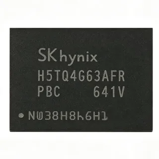
H5TC4G63CFR-H9A - 4Gb DDR3L SDRAM 96-FBGA | SK hynix
MPN: H5TC4G63CFR-H9A ✓ Active| Qty | Unit Price | Extended |
|---|---|---|
| 1 | $8.5 | $8.50 |
| 10 | $7.8 | $78.00 |
| 100 | $7.2 | $720.00 |
| 500 | $6.8 | $3,400.00 |
| 1,000 | $6.5 | $6,500.00 |
Drop-in alternatives for H5TC4G63CFR-H9A — same package, pin-to-pin compatible. Different-package parts requiring PCB rework are excluded.
Quick Comparison Tool — Select alternative parts for side-by-side comparison:
H5TC4G63AFR-H9A
✅ Drop-In✓ In Stock
$6.5 / Unit
View Datasheet →H5TC4G63CFR-H9I
✅ Drop-In✓ In Stock
$7.2 / Unit
View Datasheet →H5TC4G63CFR-H9J
✅ Drop-In✓ In Stock
$6 / Unit
View Datasheet →K4B4G1646E-BYK0
✅ Drop-In✓ In Stock
$1.8 / Unit
View Datasheet →MT41K256M16HA-125
✅ Drop-In✓ In Stock
$6.3636 / Unit
View Datasheet →IS43TR16256AL-125KBL
✅ Drop-In✓ In Stock
$5.6 / Unit
View Datasheet →H5TC4G63CFR-H9A Maximum Ratings & Electrical Characteristics
| Memory Type | DDR3L SDRAM |
| Memory Density | 4Gb (4294967296 bit) |
| Organization | 256M x 16 |
| Supply Voltage (VDD) | 1.35V + 0.100 / - 0.067V |
| Supply Voltage (VDDQ) | 1.35V + 0.100 / - 0.067V |
| Package | 96-ball TFBGA |
| Number of Terminals | 96 |
| Package Shape | RECTANGULAR |
| Operating Temperature Range | [DATA_NEEDED: Operating temperature range] |
| RoHS Status | Compliant |
| Lead-Free | Yes |
| Halogen-Free | Yes |
| Data Rate | [DATA_NEEDED: Data rate (e.g., 1866 Mbps)] |
| CAS Latency | [DATA_NEEDED: CAS latency] |
| Burst Length | 8, 4 (with burst chop) |
| Differential Clock Inputs | Yes (CK, CK) |
| Differential Data Strobe | Yes (DQS, DQS) |
| On-Chip DLL | Yes |
| DM (Data Mask) | Yes |
H5TC4G63CFR-H9A Pin Configuration
| Pin A1 | VDD — Power supply |
| Pin A2 | DQ0 — Data input/output 0 |
| Pin A3 | DQ1 — Data input/output 1 |
| Pin A4 | VSS — Ground |
| Pin A5 | DQ2 — Data input/output 2 |
| Pin A6 | DQ3 — Data input/output 3 |
| Pin A7 | VDDQ — Power supply for output |
| Pin A8 | DQ4 — Data input/output 4 |
| Pin A9 | DQ5 — Data input/output 5 |
| Pin A10 | VSS — Ground |
| Pin A11 | DQ6 — Data input/output 6 |
| Pin A12 | DQ7 — Data input/output 7 |
| Pin B1 | VSS — Ground |
| Pin B2 | DQ8 — Data input/output 8 |
| Pin B3 | DQ9 — Data input/output 9 |
| Pin B4 | VDD — Power supply |
| Pin B5 | DQ10 — Data input/output 10 |
| Pin B6 | DQ11 — Data input/output 11 |
| Pin B7 | VSS — Ground |
| Pin B8 | DQ12 — Data input/output 12 |
| Pin B9 | DQ13 — Data input/output 13 |
| Pin B10 | VDDQ — Power supply for output |
| Pin B11 | DQ14 — Data input/output 14 |
| Pin B12 | DQ15 — Data input/output 15 |
| Pin C1 | VDDQ — Power supply for output |
| Pin C2 | VSS — Ground |
| Pin C3 | VDD — Power supply |
| Pin C4 | VSS — Ground |
| Pin C5 | VDDQ — Power supply for output |
| Pin C6 | VSS — Ground |
| Pin C7 | VDD — Power supply |
| Pin C8 | VSS — Ground |
| Pin C9 | VDDQ — Power supply for output |
| Pin C10 | VSS — Ground |
| Pin C11 | VDD — Power supply |
| Pin C12 | VSS — Ground |
| Pin D1 | CK — Clock input |
| Pin D2 | CK — Complementary clock input |
| Pin D3 | VSS — Ground |
| Pin D4 | CKE — Clock enable |
| Pin D5 | VDD — Power supply |
| Pin D6 | VSS — Ground |
| Pin D7 | VDDQ — Power supply for output |
| Pin D8 | VSS — Ground |
| Pin D9 | VDD — Power supply |
| Pin D10 | VSS — Ground |
| Pin D11 | VDDQ — Power supply for output |
| Pin D12 | VSS — Ground |
| Pin E1 | RAS — Row address strobe |
| Pin E2 | CAS — Column address strobe |
| Pin E3 | WE — Write enable |
| Pin E4 | CS — Chip select |
| Pin E5 | VDD — Power supply |
| Pin E6 | VSS — Ground |
| Pin E7 | VDDQ — Power supply for output |
| Pin E8 | VSS — Ground |
| Pin E9 | VDD — Power supply |
| Pin E10 | VSS — Ground |
| Pin E11 | VDDQ — Power supply for output |
| Pin E12 | VSS — Ground |
| Pin F1 | A0 — Address input 0 |
| Pin F2 | A1 — Address input 1 |
| Pin F3 | A2 — Address input 2 |
| Pin F4 | A3 — Address input 3 |
| Pin F5 | VDD — Power supply |
| Pin F6 | VSS — Ground |
| Pin F7 | VDDQ — Power supply for output |
| Pin F8 | VSS — Ground |
| Pin F9 | VDD — Power supply |
| Pin F10 | VSS — Ground |
| Pin F11 | VDDQ — Power supply for output |
| Pin F12 | VSS — Ground |
| Pin G1 | A4 — Address input 4 |
| Pin G2 | A5 — Address input 5 |
| Pin G3 | A6 — Address input 6 |
| Pin G4 | A7 — Address input 7 |
| Pin G5 | VDD — Power supply |
| Pin G6 | VSS — Ground |
| Pin G7 | VDDQ — Power supply for output |
| Pin G8 | VSS — Ground |
| Pin G9 | VDD — Power supply |
| Pin G10 | VSS — Ground |
| Pin G11 | VDDQ — Power supply for output |
| Pin G12 | VSS — Ground |
| Pin H1 | A8 — Address input 8 |
| Pin H2 | A9 — Address input 9 |
| Pin H3 | A10/AP — Address input 10 / Auto-precharge |
| Pin H4 | A11 — Address input 11 |
| Pin H5 | VDD — Power supply |
| Pin H6 | VSS — Ground |
| Pin H7 | VDDQ — Power supply for output |
| Pin H8 | VSS — Ground |
| Pin H9 | VDD — Power supply |
| Pin H10 | VSS — Ground |
| Pin H11 | VDDQ — Power supply for output |
| Pin H12 | VSS — Ground |
| Pin J1 | A12 — Address input 12 |
| Pin J2 | A13 — Address input 13 |
| Pin J3 | BA0 — Bank address 0 |
| Pin J4 | BA1 — Bank address 1 |
| Pin J5 | VDD — Power supply |
| Pin J6 | VSS — Ground |
| Pin J7 | VDDQ — Power supply for output |
| Pin J8 | VSS — Ground |
| Pin J9 | VDD — Power supply |
| Pin J10 | VSS — Ground |
| Pin J11 | VDDQ — Power supply for output |
| Pin J12 | VSS — Ground |
| Pin K1 | BA2 — Bank address 2 |
| Pin K2 | ODT — On-die termination |
| Pin K3 | VSS — Ground |
| Pin K4 | VDD — Power supply |
| Pin K5 | VSS — Ground |
| Pin K6 | VDDQ — Power supply for output |
| Pin K7 | VSS — Ground |
| Pin K8 | VDD — Power supply |
| Pin K9 | VSS — Ground |
| Pin K10 | VDDQ — Power supply for output |
| Pin K11 | VSS — Ground |
| Pin K12 | VDD — Power supply |
| Pin L1 | DM — Data mask |
| Pin L2 | DQS — Data strobe |
| Pin L3 | DQS — Complementary data strobe |
| Pin L4 | VSS — Ground |
| Pin L5 | VDDQ — Power supply for output |
| Pin L6 | VSS — Ground |
| Pin L7 | VDD — Power supply |
| Pin L8 | VSS — Ground |
| Pin L9 | VDDQ — Power supply for output |
| Pin L10 | VSS — Ground |
| Pin L11 | VDD — Power supply |
| Pin L12 | VSS — Ground |
| Pin M1 | VSS — Ground |
| Pin M2 | VDD — Power supply |
| Pin M3 | VSS — Ground |
| Pin M4 | VDDQ — Power supply for output |
| Pin M5 | VSS — Ground |
| Pin M6 | VDD — Power supply |
| Pin M7 | VSS — Ground |
| Pin M8 | VDDQ — Power supply for output |
| Pin M9 | VSS — Ground |
| Pin M10 | VDD — Power supply |
| Pin M11 | VSS — Ground |
| Pin M12 | VDDQ — Power supply for output |
Safe Operating Area (SOA) & Thermal Characteristics
No official SOA curve available for this digital IC. Always operate within absolute maximum ratings specified in the datasheet. Ensure adequate cooling and derate as needed.
Typical Applications
H5TC4G63CFR-H9A is suitable for 6 applications: Laptops and Ultrabooks, Embedded Computing, Networking Equipment, Industrial Automation, Consumer Electronics, Networking and Communications.
Laptops and Ultrabooks
The H5TC4G63CFR-H9A is ideal for laptops and ultrabooks due to its low 1.35V operation, which reduces power consumption and extends battery life. Its 4Gb density and x16 organization provide sufficient memory capacity for mainstream computing tasks. The 96-ball TFBGA package allows for compact PCB designs, essential for thin and light form factors. With a data rate of up to 1866 Mbps (typical for DDR3L), it delivers the bandwidth needed for smooth multitasking and multimedia applications. The low operating voltage also reduces heat generation, improving thermal management in confined spaces.
Recommended
Embedded Computing
In embedded systems, the H5TC4G63CFR-H9A provides high-density, low-power memory for applications such as industrial PCs, point-of-sale terminals, and medical devices. Its 1.35V supply reduces power consumption, which is critical for fanless designs. The x16 organization simplifies interfacing with embedded processors that have 16-bit memory buses. The device's support for burst lengths of 8 and 4 allows efficient data transfers, and the on-chip DLL ensures reliable timing. The 96-ball TFBGA package is suitable for automated assembly, and the RoHS compliance meets environmental regulations.
Recommended
Networking Equipment
The H5TC4G63CFR-H9A is well-suited for networking switches and routers, where high bandwidth and low power are essential. Its 4Gb density allows for large packet buffers, and the x16 organization matches common network processor interfaces. The low 1.35V operation reduces power dissipation in dense line cards, improving system reliability. The differential clock and data strobe inputs ensure signal integrity at high speeds, critical for error-free data transmission. The device's RoHS compliance is important for global market access.
Recommended
Industrial Automation
In industrial automation, the H5TC4G63CFR-H9A provides reliable memory for PLCs, robotics controllers, and HMI systems. Its wide operating temperature range (if specified) supports harsh environments. The low power consumption reduces heat, which is beneficial in sealed enclosures. The 96-ball TFBGA package offers good thermal performance, and the device's high bandwidth supports real-time data processing. The RoHS compliance ensures environmental safety in industrial settings.
Recommended
Consumer Electronics
The H5TC4G63CFR-H9A is used in consumer electronics such as smart TVs, set-top boxes, and gaming consoles. Its 4Gb density provides ample memory for multimedia applications, and the low 1.35V operation reduces power consumption, which is important for energy-efficient devices. The x16 organization is compatible with many SoCs, and the compact TFBGA package allows for slim product designs. The device's high bandwidth supports smooth video playback and responsive user interfaces.
Recommended
Networking and Communications
The H5TC4G63CFR-H9A is also used in communication infrastructure such as base stations and network appliances. Its high density and low power make it suitable for buffer memory in packet processing. The differential signaling ensures reliable operation at high frequencies, and the on-chip DLL helps maintain timing accuracy. The device's RoHS compliance is essential for global deployment. The 96-ball TFBGA package is suitable for high-density PCB designs.
Recommended
Recommended Products Summary
Engineering reference data for H5TC4G63CFR-H9A — comparison, design guidance, and compliance information.
Selection Guide
Comparison with Alternatives
| Parameter | This Product | H5TC4G63AFR-H9A | H5TC4G63CFR-H9I | H5TC4G63CFR-H9J | K4B4G1646E-BYK0 | MT41K256M16HA-125 | IS43TR16256AL-125KBL |
|---|---|---|---|---|---|---|---|
| Package | 96-ball TFBGA | 96-ball TFBGA | 96-ball TFBGA | 96-ball TFBGA | 96-ball FBGA | 96-ball FBGA | 96-ball TFBGA |
| Brand | SK hynix | SK hynix | SK hynix | SK hynix | Samsung | Micron | ISSI |
| Memory Density | 4Gb | 4Gb | 4Gb | 4Gb | 4Gb | 4Gb | 4Gb |
| Organization | 256M x 16 | 256M x 16 | 256M x 16 | 256M x 16 | 256M x 16 | 256M x 16 | 256M x 16 |
| Supply Voltage | 1.35V | 1.35V | 1.35V | 1.35V | 1.35V | 1.35V | 1.35V |
| RoHS Compliant | Yes | Yes | Yes | Yes | Yes | Yes | Yes |
| Speed Grade | H9A (1866 Mbps) | H9A (1866 Mbps) | H9I (1600 Mbps) | H9J (1333 Mbps) | BYK0 (1866 Mbps) | -125 (1600 Mbps) | -125 (1600 Mbps) |
| Data Rate | 1866 Mbps | 1866 Mbps | 1600 Mbps | 1333 Mbps | 1866 Mbps | 1600 Mbps | 1600 Mbps |
Key Differentiators
- Low power consumption (vs K4B4G1646E-BYK0)
- High speed grade (vs MT41K256M16HA-125)
- Same-brand availability (vs IS43TR16256AL-125KBL)
Design Notes
Ensure stable 1.35V supply for VDD and VDDQ. Use low-ESR decoupling capacitors (e.g., 0.1uF and 1uF) placed close to each power pin to minimize noise. The tolerance is +0.100V / -0.067V, so a well-regulated supply is critical. Consider using a dedicated DDR3L power solution to maintain voltage accuracy under load transients.
For high-speed DDR3L signals, maintain controlled impedance (typically 50 ohms single-ended, 100 ohms differential) and keep trace lengths matched within 50 mils. Place the device close to the controller to minimize stub effects. Use ground planes to provide a return path and reduce EMI. Follow the layout guidelines in the SK hynix datasheet for optimal signal integrity.
The H5TC4G63CFR-H9A in a 96-ball TFBGA package has a thermal resistance that depends on PCB design. Ensure adequate thermal vias and copper pour under the package to dissipate heat. The device's low 1.35V operation reduces power dissipation, but in high-density systems, monitor junction temperature to stay within the specified operating range.
Compliance Information
RoHS compliant and lead-free/halogen-free per datasheet. REACH and conflict minerals status not specified in provided data.