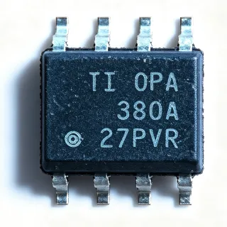
INA118UB/2K5 - Precision Low Power Instrumentation Amp | TI
MPN: INA118UB/2K5 ✓ Active| Qty | Unit Price | Extended |
|---|---|---|
| 1 | $13.5 | $13.50 |
| 10 | $12.9 | $129.00 |
| 100 | $12.69 | $1,269.00 |
| 500 | $12.2 | $6,100.00 |
| 1,000 | $11.8 | $11,800.00 |
INA118UB/2K5 Overview
An instrumentation amplifier is a specialized differential amplifier designed to amplify the difference between two input signals while rejecting common-mode noise. Within the signal-chain hierarchy, it sits above general-purpose operational amplifiers: an in-amp -> differential amplifier -> amplifier -> analog front end. Its three-op-amp architecture provides a high-impedance, internally balanced input stage, making it indispensable wherever small sensor signals ride on large common-mode voltages.
Key features of the INA118 include a gain range of 1 V/V to 10000 V/V set by a single external resistor, input protection to plus or minus 40 V, and a wide supply range from +-1.35 V up to +-18 V. Its current-feedback input circuitry preserves bandwidth at high gain, delivering 70 kHz of bandwidth even at a gain of 100, which distinguishes it from classic three-op-amp designs whose bandwidth collapses at high gains.
Technically, the INA118 uses a current-feedback input topology with internal input protection diodes. The low offset drift of 0.5 uV per degree Celsius (maximum) ensures accuracy over the industrial temperature range, while the 350 uA quiescent current suits battery-powered and loop-powered instruments. The gain equation is G = 1 + (50 kOhm / RG), where RG is the gain-setting resistor between pins 1 and 8.
Typical applications include bridge amplifiers for load cells and strain gauges, thermocouple and RTD signal conditioning, medical instrumentation front ends, and industrial process-control transmitters. The SOIC-8 footprint and wide supply range make it a drop-in fit for legacy sensor boards.
When designing, choose 1 percent or better low-drift resistors for the gain network since gain error dominates total accuracy at high gains, and keep the REF pin driven from a low-impedance source to preserve CMR.
This page synthesizes distributor pricing from DigiKey, Mouser, and LCSC, verified drop-in alternatives, and practical design notes not found in the manufacturer datasheet. Pricing is as of 2026-09-13.
Drop-in alternatives for INA118UB/2K5 — same package, pin-to-pin compatible. Different-package parts requiring PCB rework are excluded.
Variants in this series
Same-series models that are drop-in compatible with INA118UB/2K5 (same form factor and footprint) — differing in Gain Range, Operating Temperature Range, Package, Supply Voltage Range, Offset Drift (max).
Quick Comparison Tool — Select alternative parts for side-by-side comparison:
INA118UB
✅ Drop-In✓ In Stock
$16.9 / Unit
View Datasheet →INA118U/2K5
✅ Drop-In✓ In Stock
$3.3 / Unit
View Datasheet →INA818AID
✅ Drop-In📋 Reference alternative (not in catalog)
AD620ARZ
✅ Drop-In✓ In Stock
$7.2 / Unit
View Datasheet →INA128UA
✅ Drop-In📋 Reference alternative (not in catalog)
INA118UB/2K5 Maximum Ratings & Electrical Characteristics
| Amplifier Type | Instrumentation Amplifier |
| Number of Channels | 1 |
| Input Offset Voltage (max) | 50 uV |
| Offset Drift (max) | 0.5 uV/C |
| Input Bias Current (max) | 5 nA |
| Common-Mode Rejection Ratio (min) | 110 dB |
| Input Protection | +-40 V |
| Supply Voltage Range | +-1.35 V to +-18 V (2.7 V to 36 V single) |
| Quiescent Current | 350 uA |
| Gain Range | 1 V/V to 10000 V/V (single resistor set) |
| Bandwidth at G = 100 | 70 kHz |
| Operating Temperature Range | -40C to +125C |
| Package | 8-SOIC (D) |
| Mounting Type | Surface Mount |
| Packaging | Tape & Reel, 2500 units |
| Typical Dual Supply Voltage | +-15 V |
INA118UB/2K5 Pin Configuration
| Pin 1 | RG — Gain resistor terminal A |
| Pin 2 | VIN- — Inverting input |
| Pin 3 | VIN+ — Non-inverting input |
| Pin 4 | V- — Negative supply |
| Pin 5 | REF — Reference voltage for output offset (drive from low impedance) |
| Pin 6 | VOUT — Amplifier output |
| Pin 7 | V+ — Positive supply |
| Pin 8 | RG — Gain resistor terminal B |
Typical Applications
INA118UB/2K5 is suitable for 6 applications: Load Cell and Weigh-Scale Bridge Amplifier, Thermocouple Signal Conditioning, 4-20 mA Loop-Powered Transmitters, Medical Biopotential Front End (ECG/EEG), Industrial Process Control and PLC Analog Input, Strain Gauge and Pressure Sensor Signal Conditioning.
Load Cell and Weigh-Scale Bridge Amplifier
The INA118UB/2K5 is a natural fit for load-cell bridge amplification because its 50 uV maximum offset and 0.5 uV per degree Celsius drift preserve resolution of microvolt-level bridge outputs, while the 110 dB minimum CMR rejects ground noise between the weigh platform and the electronics. A typical 2 mV/V load cell excited at 5 V produces only 10 mV full scale; with a gain of 200 (RG = 251 Ohm per the TI gain equation G = 1 + 50 kOhm/RG), the 70 kHz bandwidth at G = 100 comfortably covers filtering needs. Placed directly at the bridge with a precision 1 percent low-drift gain resistor, it converts the differential bridge signal to a ground-referenced single-ended output for an ADC such as the CS5532. The 350 uA quiescent current permits battery-powered portable scales.
Recommended
Thermocouple Signal Conditioning
Thermocouples generate only tens of microvolts per degree Celsius (about 41 uV per degree C for type K), so amplifier offset and drift dominate measurement error. The INA118UB/2K5's 50 uV maximum offset corresponds to roughly 1.2 degrees C of equivalent error, and the 0.5 uV per degree Celsius drift keeps error growth negligible across the -40C to +125C industrial range. Its 5 nA maximum input bias current prevents loading of high-impedance thermocouple junctions, and the internal +-40 V input protection survives wiring faults and induced surges common on long thermocouple runs in furnaces and process plants. With a gain of approximately 244 (RG = 206 Ohm), a type-K signal spans most of a 3.3 V or 5 V ADC input range. Combine with cold-junction compensation, such as a TMP or analog temperature sensor on the connector block, for full accuracy.
Recommended
4-20 mA Loop-Powered Transmitters
The INA118UB/2K5's 350 uA quiescent current and 2.7 V minimum single-supply operation make it suitable for 4-20 mA current-loop transmitters where the entire sensor head must fit within the loop budget, often under 1 mA. In a typical two-wire transmitter, the in-amp amplifies a differential sensor signal (RTD, strain gauge, or pressure bridge) and drives a voltage-to-current converter that modulates loop current. The wide supply range up to 36 V directly tolerates the loop compliance voltage, and the 110 dB CMR rejects common-mode potential differences between the remote sensor ground and the receiver. According to TI datasheet guidance, the REF pin can be driven to bias the output for unipolar sensor spans, and the 70 kHz bandwidth at high gain leaves ample margin over the low loop-update rates typical in process control.
Recommended
Medical Biopotential Front End (ECG/EEG)
Biopotential signals such as ECG (0.5 mV to 4 mV) and EEG (tens of microvolts) demand amplifiers with low offset, low bias current, and very high common-mode rejection to reject 50/60 Hz mains interference coupled through the body. The INA118UB/2K5's 110 dB minimum CMR and 5 nA maximum input bias current address exactly these requirements, while the +-40 V input protection provides defibrillation-tolerant resilience when paired with external series resistors and clamp diodes, a topology shown in the TI datasheet medical applications. A gain of 10 to 100 at the in-amp stage (70 kHz bandwidth at G = 100 leaves huge margin over the sub-kHz physiologically relevant band) followed by a high-pass filter and further gain in a precision op amp such as the OPA2277 delivers a clean signal to the ADC. Low 350 uA consumption supports portable patient monitors.
Recommended
Industrial Process Control and PLC Analog Input
Programmable logic controller analog input modules must amplify differential sensor signals that ride on large common-mode voltages and survive miswiring. The INA118UB/2K5's +-40 V input protection exceeds typical 24 V industrial rail potentials, guarding the front end against accidental direct connection to supply or signal lines, a common field failure mode. Its 2.7 V to 36 V supply range allows the in-amp to run directly from the module's 24 V rail or a +-15 V analog rail without a dedicated regulator stage. The 50 uV maximum offset supports 12-bit to 16-bit accuracy targets after calibration, and the 110 dB CMR maintains accuracy despite ground potential differences of several volts across a factory floor. The SOIC-8 package fits dense multiplexed input channel boards using an analog multiplexer ahead of the in-amp.
Recommended
Strain Gauge and Pressure Sensor Signal Conditioning
Strain gauge and piezoresistive pressure bridges output differential signals in the millivolt range superimposed on large common-mode excitation voltage, precisely the condition for which the INA118UB/2K5's three-op-amp architecture is designed. With a gain of 500 to 1000 (RG = 50.5 to 100.2 Ohm per the TI gain equation), full-bridge outputs of 2 mV to 10 mV map to standard 2.5 V to 5 V ADC spans. The 0.5 uV per degree Celsius maximum drift converts to bridge-referred error of only a few microvolts over the industrial range, critical for long-term pressure measurement stability. TI's datasheet shows a typical bridge amplifier circuit using the REF pin for offsetting. The 5 nA bias current is negligible against typical 350 Ohm bridge impedances, avoiding gain error from source-impedance imbalance.
Recommended
Recommended Products Summary
Engineering reference data for INA118UB/2K5 — comparison, design guidance, and compliance information.
Selection Guide
Comparison with Alternatives
| Parameter | This Product | INA118UB | INA118U/2K5 | INA818AID | AD620AR | INA128UA |
|---|---|---|---|---|---|---|
| Package | 8-SOIC (D) | 8-SOIC (D) - same | 8-SOIC (D) - same | 8-SOIC (D) - same | SOIC-8 - same footprint | 8-SOIC (D) - same |
| Brand | Texas Instruments | Texas Instruments | Texas Instruments | Texas Instruments | Analog Devices | Texas Instruments |
| Input Bias Current (max) | 5 nA | 5 nA | 5 nA | 0.5 nA | 2 nA (typ 1 nA) | 5 nA |
| Quiescent Current | 350 uA | 350 uA | 350 uA | 350 uA | 1.3 mA | 700 uA |
| Input Protection | +-40 V | +-40 V | +-40 V | +-40 V (per INA818 datasheet) | +-40 V | +-40 V |
| Temperature Range | -40C to +125C | -40C to +125C | -40C to +85C (per family spec) | -40C to +125C | -40C to +85C | -40C to +85C |
Key Differentiators
- Bandwidth preserved at high gain (vs AD620AR)
- Lower power for loop-powered designs (vs AD620AR)
- Drop-in upgrade path to better accuracy (vs INA818AID)
- Wider operating temperature range (vs INA118U/2K5)
Design Notes
Always drive the REF pin (pin 5) from a low-impedance source, such as an op-amp buffer or directly to ground. Any resistance in series with REF degrades the INA118's 110 dB common-mode rejection by a factor proportional to the gain. A common field mistake is tying REF to a resistor divider for output offsetting; buffer the divider instead with a precision op amp such as the OPA2277 to preserve CMR and offset accuracy.
The gain-setting resistor RG between pins 1 and 8 sets gain via G = 1 + 50 kOhm/RG; any series resistance in the RG trace adds directly to RG and creates gain error. At a gain of 1000 (RG = 50.1 Ohm), just 0.5 Ohm of trace resistance causes roughly 1 percent gain error. Place RG close to the device with short, direct traces, use 1 percent or better 25 ppm per degree Celsius resistors, and keep RG away from switching nodes to avoid noise pickup.
Decouple both supply pins with 0.1 uF ceramic capacitors placed within 2 mm of pins 4 and 7, plus a 2.2 uF to 10 uF bulk capacitor on the rail. Although the INA118 draws only 350 uA, the 2.7 V minimum supply means upstream regulators must maintain headroom at load; for 4-20 mA loop-powered designs, budget the 350 uA in-amp consumption plus regulator quiescent current inside the roughly 1 mA loop headroom to avoid dropping out of regulation at low loop current.
For long sensor cables, add a differential RC filter (for example 1 kOhm plus 10 nF per input, matched 1 percent) before pins 2 and 3 to limit RF pickup and protect the amplifier. Matched resistors preserve the 110 dB CMR; mismatch converts common-mode noise to differential error. Estimated: a 1 percent resistor mismatch on a 1 V common-mode step introduces roughly 5 mV equivalent differential, which dominates the 50 uV offset budget - precision matching matters more than the amplifier choice.
Compliance Information
Compliance status not explicitly stated in the provided verified web data; consult the TI product page for RoHS/REACH certificates.