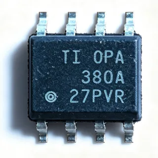
OPA206 - 240uA Low-Noise Precision Op Amp, OVP | TI
MPN: OPA206 ✓ Active| Qty | Unit Price | Extended |
|---|---|---|
| 1 | $2.95 | $2.95 |
| 10 | $2.65 | $26.50 |
| 100 | $2.25 | $225.00 |
| 500 | $1.95 | $975.00 |
| 1,000 | $1.72 | $1,720.00 |
OPA206 Overview
A precision operational amplifier is a high-accuracy analog amplifier within the hierarchy of operational amplifiers, amplifier ICs, and analog signal chain semiconductors. Precision op amps minimize DC error sources - input offset voltage, offset drift, and input bias current - so small sensor and reference signals can be amplified faithfully in instrumentation, data acquisition, and control systems.
Key features include a maximum input offset voltage of 25 uV (e-trim calibrated), a maximum offset voltage drift of 0.5 uV/degC, and a maximum input bias current of 500 pA enabled by super-beta input transistors. The integrated OVP protects inputs up to 40 V beyond the supplies - a feature few precision op amps offer - eliminating external clamp diode networks that add leakage and noise. The push-pull, rail-to-rail output stage maximizes dynamic range on low supply rails.
The OPAx206 family is positioned by TI as the next generation of the industry-standard OPAx277 family, retaining low-drift precision character while adding OVP. E-trim factory trimming removes the dominant offset error at manufacture, achieving temperature stability that discrete trimming cannot easily match. According to the TI datasheet, the family spans single (OPA206), dual (OPA2206), and quad (OPA4206) versions for design scalability.
Typical applications include transducer signal conditioning, precision data-acquisition front ends, industrial PLC analog input modules, test-and-measurement instrumentation, and battery-powered precision systems where 240 uA quiescent current conserves power. Supply operation from 4.5 V to 36 V total suits both 5 V single-supply and plus/minus 15 V dual-supply systems.
Design consideration: choose the OPA206 when inputs may be exposed to fault voltages; if inputs are inherently protected and minimum noise is paramount, the pin-compatible OPA205 offers slightly better noise without OVP.
Drop-in alternatives for OPA206 — same package, pin-to-pin compatible. Different-package parts requiring PCB rework are excluded.
Variants in this series
Same-series models that are drop-in compatible with OPA206 (same form factor and footprint) — differing in Package, Input Bias Current, Input Voltage Noise Density, Number of Channels.
Quick Comparison Tool — Select alternative parts for side-by-side comparison:
OPA205AID
✅ Drop-In📋 Reference alternative (not in catalog)
OPA277AID
✅ Drop-In📋 Reference alternative (not in catalog)
OPA2206AID
⚡ Same Package📋 Reference alternative (not in catalog)
ADA4522-1ARZ
✅ Drop-In ⚠️ Specs Unverified✓ In Stock
$1.42 / Unit
View Datasheet →OPA2192IDR
✅ Drop-In ⚠️ Specs Unverified✓ In Stock
$0.82 / Unit
View Datasheet →OPA206 Maximum Ratings & Electrical Characteristics
| Channels | 1 |
| Quiescent Current (per amp) | 240 uA |
| Input Voltage Noise Density | 8 nV/rtHz |
| Input Offset Voltage (max) | 25 uV |
| Offset Voltage Drift (max) | +/-0.5 uV/degC |
| Input Bias Current (max) | 500 pA |
| Input Overvoltage Protection | Up to +/-40 V beyond supplies |
| Supply Voltage Range (total) | 4.5 V to 36 V |
| Output Stage | Push-pull, rail-to-rail |
| Trim Technology | e-trim(TM) factory calibration |
| Input Type | Super-beta inputs |
| Package | 8-SOIC (D) |
| Mounting Type | Surface Mount |
| RoHS Status | Compliant |
| Family | OPAx206 (single/dual/quad: OPA206, OPA2206, OPA4206) |
OPA206 Pin Configuration
| Pin 1 | TRIM — Offset trim adjustment (see TI datasheet) |
| Pin 2 | -IN — Inverting input (OVP protected to 40 V beyond rails) |
| Pin 3 | +IN — Non-inverting input (OVP protected to 40 V beyond rails) |
| Pin 4 | V- — Negative supply |
| Pin 5 | TRIM — Offset trim adjustment (see TI datasheet) |
| Pin 6 | OUT — Rail-to-rail push-pull output |
| Pin 7 | V+ — Positive supply |
| Pin 8 | N/C or TRIM — [DATA_NEEDED: pin 8 function per datasheet] |
Typical Applications
OPA206 is suitable for 6 applications: Precision Data-Acquisition Front End, Industrial PLC Analog Input Modules, Battery-Powered Precision Instrumentation, Transducer Signal Conditioning, Test and Measurement Instrumentation, Medical Diagnostic Signal Chains.
Precision Data-Acquisition Front End
The OPA206's 25 uV maximum offset, 0.5 uV/degC drift, and 8 nV/rtHz noise preserve small sensor signals ahead of precision ADCs. Its integrated 40 V OVP protects front ends from field wiring faults, and 240 uA quiescent current keeps channel power low. Place the OPA206 directly before the ADC input driver with gain set by low-TC resistors; unlike externally protected designs, no clamp diodes add leakage, improving low-level accuracy across temperature.
Recommended
Industrial PLC Analog Input Modules
In PLC analog inputs, field terminals can be hit by miswiring or transient voltages far beyond the supply rails. The OPA206's input OVP up to 40 V beyond either rail survives these faults without external diode networks, while 36 V total supply range suits +/-15 V industrial rails. Its 25 uV offset maintains accuracy for 4-20 mA sense conditioning across channel-to-channel variations, and the push-pull rail-to-rail output drives downstream filtering stages at full dynamic range.
Recommended
Battery-Powered Precision Instrumentation
Portable and battery-powered instruments benefit from the OPA206's 240 uA per-amplifier quiescent current, which extends battery life versus classic precision op amps drawing milliamps. With 8 nV/rtHz noise and 500 pA maximum bias current from super-beta inputs, it conditions high-impedance sensors without significant signal error. Operation from 4.5 V total supply supports single Li-ion or 5 V rails, and e-trim factory calibration removes offset trimming steps from production test, lowering system cost.
Recommended
Transducer Signal Conditioning
Strain gauges, thermocouple amplifiers, and bridge transducers produce millivolt-level outputs where offset and drift dominate total error. The OPA206's 25 uV maximum offset and 0.5 uV/degC drift keep DC errors below 0.1 percent of a 25 mV full-scale bridge output over a wide temperature span. Super-beta inputs (500 pA max bias) limit bridge loading, and integrated OVP guards against lead misconnection. A single SOIC-8 per channel simplifies dense multi-channel conditioning boards.
Recommended
Test and Measurement Instrumentation
Bench instruments and automated test equipment require low noise and stable gain. The OPA206's 8 nV/rtHz broadband noise supports low-noise gain stages, while e-trim calibration guarantees repeatable offset channel-to-channel - important for calibrator product families. The 36 V supply range fits +/-15 V analog architectures common in TME designs, and OVP tolerates operator misconnection at instrument inputs up to 40 V beyond the rails, improving product robustness in field service.
Recommended
Medical Diagnostic Signal Chains
Medical diagnostic equipment such as patient-monitoring analog front ends demands low noise, low drift, and robust input protection. The OPA206's 8 nV/rtHz noise preserves biosignal fidelity, 500 pA bias current limits electrode polarization artifacts, and the 40 V OVP adds a defibrillation-adjacent protection layer at the amplifier input stage. At 240 uA, it suits portable medical devices; e-trim offset stability reduces recalibration frequency across service intervals.
Recommended
Recommended Products Summary
Engineering reference data for OPA206 — comparison, design guidance, and compliance information.
Selection Guide
Comparison with Alternatives
| Parameter | This Product | OPA205AID | OPA277AID | ADA4522-1 |
|---|---|---|---|---|
| Package | 8-SOIC (D) | 8-SOIC (D) - same | 8-SOIC (D) - same | 8-SOIC (D) - same footprint |
| Brand | Texas Instruments | Texas Instruments | Texas Instruments | Analog Devices |
| Input OVP | +/-40 V beyond rails | None | None | None |
| Channels | 1 | 1 | 1 | 1 |
Key Differentiators
- Integrated input OVP to 40 V beyond rails (vs OPA205AID)
- Next-generation OPAx277 with lower power (vs OPA277AID)
- Factory e-trim calibration stability (vs ADA4522-1)
Design Notes
Do not assume OVP replaces full ESD/fault strategy: the integrated protection covers inputs up to 40 V beyond the supplies, but continuous overvoltage still injects current into the rails - size supply rails and ensure a defined fault current path per the TI OPA206 datasheet. Also, the OVP clamps add small input current under normal operation; for picoampere-level bias applications verify total error budget including protection circuitry.
Place a 100 nF ceramic decoupling capacitor within 2 mm of each supply pin (V+ pin 7, V- pin 4) to ground, with a bulk 1-10 uF per supply rail. Keep the high-impedance input traces short and guard them with a driven ground ring to preserve the 500 pA bias-current accuracy. For offset trim use, follow the trim network in the TI datasheet typical application rather than the legacy OPAx277 trim circuit.
At 8 nV/rtHz input noise, source impedance contributes Johnson noise: a 100 kohm source adds about 40 nV/rtHz and dominates. Keep source resistances below ~1 kohm for noise-critical gain stages, and set gains so the amplifier output, not the source, defines the signal chain noise floor. The rail-to-rail push-pull output can drive modest loads directly, but check headroom near rails at the required load current.
Compliance Information
RoHS compliant per TI product page. REACH/halogen/conflict-minerals declarations not present in provided data - see TI quality portal.