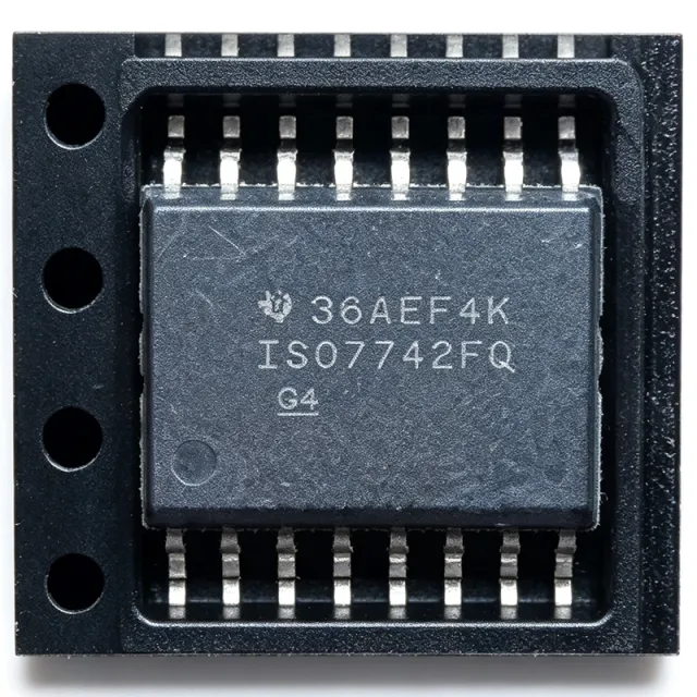
ISO7742FDBQR - Reinforced 4-Ch Digital Isolator | TI
MPN: ISO7742FDBQR ✓ Active| Qty | Unit Price | Extended |
|---|---|---|
| 1 | $3.42 | $3.42 |
| 10 | $3.08 | $30.80 |
| 100 | $2.74 | $274.00 |
| 500 | $2.47 | $1,235.00 |
| 1,000 | $2.2 | $2,200.00 |
Drop-in alternatives for ISO7742FDBQR — same package, pin-to-pin compatible. Different-package parts requiring PCB rework are excluded.
Quick Comparison Tool — Select alternative parts for side-by-side comparison:
ISO7742DBQR
✅ Drop-In📋 Reference alternative (not in catalog)
ISO7741FDBQR
✅ Drop-In✓ In Stock
$1.42 / Unit
View Datasheet →ISO7740FDBQR
✅ Drop-In📋 Reference alternative (not in catalog)
ISO7742FDBQR Maximum Ratings & Electrical Characteristics
| Number of Channels | 4 |
| Forward/Reverse Channels | 2/2 |
| Isolation Rating | 3000 Vrms (DBQ package) |
| Data Rate | 100 Mbps |
| CMTI | 85 kV/µs (min), ±100 kV/µs (typ) |
| Supply Voltage | 2.25 V to 5.5 V |
| Operating Temperature | -55°C to 125°C |
| Package | 16-SSOP (DBQ) |
| Surge Capability | 12.8 kV |
| Working Voltage | 1500 Vrms (projected lifetime >30 years) |
| Isolation Technology | Capacitive |
| Fail-Safe Output | Yes |
| RoHS | Compliant |
| Lead-Free | Yes |
| Mounting Type | Surface Mount |
ISO7742FDBQR Pin Configuration
| Pin 1 | VCC1 — Supply voltage, side 1 |
| Pin 2 | GND1 — Ground, side 1 |
| Pin 3 | INA — Input channel A |
| Pin 4 | INB — Input channel B |
| Pin 5 | OUTC — Output channel C |
| Pin 6 | OUTD — Output channel D |
| Pin 7 | GND1 — Ground, side 1 |
| Pin 8 | NC — No connect |
| Pin 9 | NC — No connect |
| Pin 10 | GND2 — Ground, side 2 |
| Pin 11 | INC — Input channel C |
| Pin 12 | IND — Input channel D |
| Pin 13 | OUTA — Output channel A |
| Pin 14 | OUTB — Output channel B |
| Pin 15 | GND2 — Ground, side 2 |
| Pin 16 | VCC2 — Supply voltage, side 2 |
Safe Operating Area (SOA) & Thermal Characteristics
No official SOA curve available for this digital IC. Always operate within absolute maximum ratings specified in the datasheet. Ensure adequate cooling and derate as needed.
Typical Applications
ISO7742FDBQR is suitable for 6 applications: Industrial Fieldbus Communication, Motor Drives, Power Inverters, Isolated SPI/UART Interfaces, Automotive Electronics, Medical Equipment.
Industrial Fieldbus Communication
The ISO7742FDBQR provides galvanic isolation for fieldbus interfaces like PROFIBUS, Modbus, and CAN. Its 100 Mbps data rate and high CMTI ensure reliable communication in noisy industrial environments. The reinforced isolation protects against ground loops and voltage transients, making it ideal for factory automation and process control systems.
Recommended
Motor Drives
In motor drive systems, the ISO7742FDBQR isolates control signals from high-voltage power stages. Its high CMTI (85 kV/µs) prevents false triggering during fast switching transients, while the reinforced isolation ensures safety. The 2/2 channel configuration is ideal for transmitting PWM signals and feedback from encoders or sensors.
Recommended
Power Inverters
The ISO7742FDBQR is used in solar inverters and UPS systems to isolate control electronics from high-voltage DC buses. Its 3000 Vrms isolation and 12.8 kV surge capability provide robust protection against lightning and switching surges. The wide supply range allows interfacing with both 3.3V and 5V microcontrollers.
Recommended
Isolated SPI/UART Interfaces
The ISO7742FDBQR provides isolation for SPI and UART communication between microcontrollers and peripherals in noisy environments. Its 100 Mbps data rate supports high-speed SPI clocks, while the fail-safe outputs ensure known states during power-up. The 2/2 channel configuration is perfect for SPI (SCLK, MOSI, MISO, CS) or UART (TX, RX) with flow control.
Recommended
Automotive Electronics
The ISO7742FDBQR is suitable for automotive applications such as battery management systems (BMS) and on-board chargers, where galvanic isolation is required between high-voltage and low-voltage domains. Its extended temperature range (-55°C to 125°C) and high CMTI ensure reliable operation in harsh automotive environments. The reinforced isolation meets safety standards for electric vehicles.
Recommended
Medical Equipment
In medical devices, the ISO7742FDBQR provides patient isolation for monitoring and diagnostic equipment. Its reinforced isolation (3000 Vrms) meets safety standards for medical applications, protecting patients from electric shock. The low power consumption and small SSOP package make it suitable for portable and wearable medical devices.
Recommended
Recommended Products Summary
Engineering reference data for ISO7742FDBQR — comparison, design guidance, and compliance information.
Selection Guide
Comparison with Alternatives
| Parameter | This Product | ISO7742DBQR | ISO7741FDBQR | ISO7740FDBQR | ISO7742DW | ADuM1402CRWZ |
|---|---|---|---|---|---|---|
| Package | 16-SSOP (DBQ) | 16-SSOP (DBQ) | 16-SSOP (DBQ) | 16-SSOP (DBQ) | 16-SOIC (DW) | 16-SOIC (RW) |
| Brand | Texas Instruments | Texas Instruments | Texas Instruments | Texas Instruments | Texas Instruments | Analog Devices |
| Number of Channels | 4 | 4 | 3 | 4 | 4 | 4 |
| Forward/Reverse Channels | 2/2 | 2/2 | 2/1 | 4/0 | 2/2 | 2/2 |
| Isolation Rating | 3000 Vrms | 3000 Vrms | 3000 Vrms | 3000 Vrms | 5000 Vrms | 2500 Vrms |
| Data Rate | 100 Mbps | 100 Mbps | 100 Mbps | 100 Mbps | 100 Mbps | 90 Mbps |
| CMTI | 85 kV/µs (min) | 85 kV/µs (min) | 85 kV/µs (min) | 85 kV/µs (min) | 85 kV/µs (min) | 25 kV/µs (min) |
| Supply Voltage | 2.25V to 5.5V | 2.25V to 5.5V | 2.25V to 5.5V | 2.25V to 5.5V | 2.25V to 5.5V | 3.0V to 5.5V |
Key Differentiators
- Reinforced isolation with 3000 Vrms rating (vs ADuM1402CRWZ)
- Higher CMTI (85 kV/µs min) (vs ADuM1402CRWZ)
- Fail-safe output feature (vs ISO7742DBQR)
Design Notes
For the ISO7742FDBQR, maintain adequate creepage and clearance distances on the PCB to preserve the 3000 Vrms isolation rating. According to TI's layout guidelines, a minimum of 8 mm creepage is recommended for reinforced isolation in pollution degree 2 environments. Place the isolation barrier gap on the PCB to separate the high-voltage and low-voltage sides.
Decouple both VCC1 and VCC2 with 0.1 µF ceramic capacitors placed as close to the pins as possible. Additionally, use a 10 µF bulk capacitor on each supply if the power source is distant. This ensures stable operation and reduces noise coupling into the isolation barrier.
Do not exceed the absolute maximum ratings, especially the supply voltage (7V) and isolation voltage. Ensure that the input signals do not exceed the supply voltage. Also, note that the fail-safe output feature (F suffix) means outputs go to a known state when the input side is unpowered; this is beneficial but must be considered in system design.
Compliance Information
RoHS compliant per TI product page. Not AEC-Q100 qualified; automotive variant ISO7742FQDWQ1 is available.




