LAST TIME BUY NOTICE: M25P10-AVMB3TP/Y is approaching end-of-life. Last order date: Contact us. View available alternative parts β†’
Micron Technology

M25P10-AVMB3TP/Y - 1Mbit SPI NOR Flash 50MHz | Micron

MPN: M25P10-AVMB3TP/Y βœ— End of Life
In Stock Ships in 1-3 business days
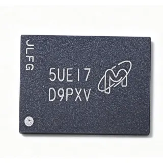
2.7 V to 3.6 V Vdss 8-UFDFPN (2x3 mm) Package 50 MHz Speed NOR Flash, Serial SPI Memory
From $0.35 USD / Unit
MOQ: 1 |
Price updated: 2026-09-04
Volume Pricing
Qty Unit Price Extended
1 $0.75 $0.75
10 $0.62 $6.20
100 $0.48 $48.00
500 $0.41 $205.00
1,000 $0.35 $350.00
ℹ️ All prices are in USD

Drop-in alternatives for M25P10-AVMB3TP/Y β€” same package, pin-to-pin compatible. Different-package parts requiring PCB rework are excluded.

Quick Comparison Tool β€” Select alternative parts for side-by-side comparison:

M25P10-AVMB6TP/Y

βœ… Drop-In ⚠️ 参数待ιͺŒθ―
πŸ“¦ 8-UFDFPN (2x3 mm)
same die and UFDFPN 2x3 mm footprint, different speed/voltage grade suffix (MB6 vs MB3) - pin-to-pin compatible

πŸ“‹ Reference alternative (not in catalog)

M25P10-AVMB3TP/Y Maximum Ratings & Electrical Characteristics

Memory Type NOR Flash, Serial SPI
Density 1 Mbit (128 Kbyte)
Organization 4 sectors of 256 Kbit
Interface SPI (serial peripheral interface)
Max Clock Frequency 50 MHz
Supply Voltage 2.7 V to 3.6 V
Page Program Time 1.4 ms typical (up to 256 bytes)
Sector Erase Time 0.8 s typical (256 Kbit sector)
Bulk Erase Time 2.5 s typical (1 Mbit)
Package 8-UFDFPN (2x3 mm)
Mounting Type Surface Mount
Write Protection Hardware (W#) and software protection
HOLD Function Yes (HOLD# pin)

M25P10-AVMB3TP/Y Pin Configuration

DFN-8 Package Pinout Diagram DFN-8 2x2mm, P0.5mm, EP 0.9x1.7mm, JEDEC MO-229. 1 8 2 7 3 6 4 5 DFN-8
Pin 1 S# β€” Chip select (active low)
Pin 2 Q β€” Serial data output (data out)
Pin 3 W# β€” Write protect (active low)
Pin 4 VSS β€” Ground
Pin 5 D β€” Serial data input (data in)
Pin 6 C β€” Serial clock
Pin 7 HOLD# β€” Hold (suspend serial communication)
Pin 8 VCC β€” Power supply (2.7 V to 3.6 V)

Safe Operating Area (SOA) & Thermal Characteristics

Safe Operating Area Chart Default safe operating area chart for M25P10-AVMB3TP/Y Drain-to-Source Voltage (Vds) Drain Current (Id)

No official SOA curve available for this digital IC. Always operate within absolute maximum ratings specified in the datasheet. Ensure adequate cooling and derate as needed.

Typical Applications

M25P10-AVMB3TP/Y is suitable for 6 applications: FPGA Configuration Storage, Embedded BIOS / Boot Code, Set-Top Box Firmware, Industrial PLC Parameter Storage, Networking Equipment Boot ROM, Display Panel and TV Controller Code.

πŸ”§

FPGA Configuration Storage

The M25P10-AVMB3TP/Y stores configuration bitstreams for small FPGAs and CPLDs that power up from serial Flash. Its 1 Mbit capacity matches the compressed configuration file size of low-density devices, while the 50 MHz SPI interface and fast-read instruction stream the bitstream quickly enough to keep configuration times in the tens of milliseconds. Because the device uses the standard M25P command set supported by virtually all FPGA configuration logic, integration requires only four signal lines plus HOLD# and W#. Designers should drive W# high during power-up so the bitstream cannot be corrupted before the FPGA completes loading, and should size the 2.7 V to 3.6 V rail with a 0.1 uF local decoupling capacitor for glitch-free streaming at 50 MHz.

πŸ–₯️

Embedded BIOS / Boot Code

Embedded x86 and MCU platforms use the M25P10-AVMB3TP/Y to hold compressed BIOS or bootloader images. The 1.4 ms typical page program time means a full 128 Kbyte image flashes in well under a second during manufacturing, and the sector-erase granularity (256 Kbit sectors in 0.8 s typical) supports in-field firmware updates without erasing the whole array. The low pin-count UFDFPN (2x3 mm) package fits beside the chipset on dense boards. The 2.7 V to 3.6 V supply range connects directly to standard 3.3 V rails, and the status-register protection scheme lets the boot ROM region be write-locked against malware or errant writes while leaving parameter sectors writable.

πŸ“Ί

Set-Top Box Firmware

Set-top boxes and IPTV clients store main firmware, channel tables, and DRM parameters in serial NOR Flash such as the M25P10-AVMB3TP/Y. The 1 Mbit array accommodates a compressed second-stage bootloader and parameter blocks, while the 50 MHz SPI clock keeps boot-to-kernel times short. Hardware write protection via the W# pin safeguards the bootloader region against accidental corruption during over-the-air updates that rewrite the application sectors. The device's standard SPI interface integrates with the main SoC's dedicated Flash controller with no glue logic, and the 2.7 V to 3.6 V single-supply operation simplifies power tree design in cost-sensitive consumer hardware.

🏭

Industrial PLC Parameter Storage

Programmable logic controllers and industrial sensors use the M25P10-AVMB3TP/Y for calibration constants, recipe data, and event logs that must survive power loss. Serial NOR provides deterministic read latency and vastly better byte-level reliability than EEPROM emulation schemes, and the sector architecture allows frequently changing parameter blocks to live in one sector while calibration constants occupy another. The 1.4 ms page program time permits logging entries without stalling the control loop, and the status-register software protection prevents corruption during brown-out events when combined with supply supervision. Its 2x3 mm footprint suits the compact DIN-rail module form factors typical of industrial I/O.

🌐

Networking Equipment Boot ROM

Switches, routers, and gateways store bootloaders and MAC/PHY configuration in SPI NOR. The M25P10-AVMB3TP/Y serves the first-stage boot role: its 50 MHz fast-read output streams the secondary loader into RAM quickly, and the 1 Mbit array holds the bootloader plus board-identity data (MAC address, serial number, hardware revision). Hardware write protection through W# makes the boot region tamper-resistant, an important requirement for network security compliance. The device operates on the same 3.3 V rail as the networking ASIC, removing level-shift circuitry, and the small UFDFPN body fits on dense line-card PCBs where board area is at a premium.

πŸ“Ί

Display Panel and TV Controller Code

LCD and TV scaler boards store scaler firmware, EDID data, and factory calibration tables in small SPI NOR Flash. The M25P10-AVMB3TP/Y's 1 Mbit array covers a compressed scaler boot block plus gamma and white-balance calibration sectors, and the 50 MHz interface supports fast panel-startup sequences demanded by quick-power-on specifications. Sector erase (0.8 s typical) lets service software update individual calibration blocks without rewriting the boot region, which remains write-protected via W#. The 2x3 mm UFDFPN package fits within the thin bezel PCB envelope of modern monitors, and the 2.7 V to 3.6 V supply matches the panel controller's 3.3 V rail directly.

What is the M25P10-AVMB3TP/Y and what are its key specifications?
The M25P10-AVMB3TP/Y is a Micron 1 Mbit serial NOR Flash memory with a 50 MHz SPI bus interface, 2.7 V to 3.6 V single supply, and page programming of up to 256 bytes in 1.4 ms typical. It comes in an 8-pin UFDFPN (2x3 mm) package. Per the manufacturer datasheet, sector erase (256 Kbit) takes 0.8 s typical and bulk erase takes 2.5 s typical.
What is the pinout of the M25P10-AVMB3TP/Y in the 8-UFDFPN package?
In the 8-UFDFPN (2x3 mm) package, the pins are: 1 = S# (chip select), 2 = Q (serial data output), 3 = W# (write protect), 4 = VSS (ground), 5 = D (serial data input), 6 = C (serial clock), 7 = HOLD# (hold), and 8 = VCC (power supply). This is the standard M25P10-A pinout shown in the datasheet pin descriptions section.
Is the M25P10-A still in production, or is it EOL?
Micron has announced end-of-life for its low-density memory solutions, including the M25P series, so the M25P10-A family is EOL / last-time-buy. Renesas publishes an official 'Conversion Guide Micron EOL M25P Products' documenting migration to Adesto FUSION and Standard Flash. Buyers should qualify alternatives or secure last-time-buy stock before supply ends.
What is the best drop-in replacement for M25P10-AVMB3TP/Y?
The closest same-family drop-in candidates are other M25P10-A speed/voltage variants in the same UFDFPN footprint, such as the M25P10-AVMB6TP/Y grade. For long-term supply, the Renesas/Adesto conversion guide for Micron EOL M25P products lists cross-brand equivalents, but package footprint and command-set compatibility must be verified on your PCB before qualification. No verified cross-brand pin-to-pin equivalent in the identical 2x3 UFDFPN package appears in current distributor cross-reference data.
Is the M25P10-AVMB3TP/Y the same as the Winbond W25X10?
No, they are functionally similar 1 Mbit SPI NOR Flash devices, but the Winbond W25X10 comes in an SOIC-8 body rather than the 2x3 mm UFDFPN of the M25P10-AVMB3TP/Y, so it is not a drop-in replacement. Command sets are also not identical byte-for-byte. Engineers should treat the W25X10 as a functional substitute requiring PCB footprint change verification, not as a pin-to-pin replacement.
Where to buy M25P10-AVMB3TP/Y online and what is the price?
The M25P10-AVMB3TP/Y TR is listed at DigiKey and via broker channels such as Octopart-partner distributors, with broker stock from sources like One River, DGT Technology, and Anterwell as of 2026-09-04. Because the part is EOL, pricing varies by broker; typical single-unit pricing is under one dollar, while broker lots carry significant premiums. Check XAIPART's current quote system for verified-stock pricing.
Is M25P10-AVMB3TP/Y in stock, and what is the lead time?
Distributor stock exists in limited quantity: DigiKey lists the TR variant, and brokers report quantities such as 31,000 units (One River) and 28,040 units (Anterwell) as of mid-2025 listings. Since the part is EOL, lead time is broker-dependent, typically days for stock lots and weeks for scheduled deliveries. Confirm authenticity certification when buying from brokers, as EOL parts carry counterfeit risk.
What supply voltage does the M25P10-AVMB3TP/Y require?
The M25P10-AVMB3TP/Y operates from a single 2.7 V to 3.6 V supply, per the manufacturer datasheet. This makes it directly compatible with standard 3.0 V and 3.3 V rails, and the 'V' in the part number denotes this extended low-voltage operating range relative to earlier 2.7 V-fixed M25P generations.
How fast is the M25P10-A page program and erase cycle?
According to the manufacturer datasheet, the M25P10-A programs up to 256 bytes per page in 1.4 ms typical, erases a 256 Kbit sector in 0.8 s typical, and performs a bulk erase of the full 1 Mbit array in 2.5 s to 4 s typical. These timings allow a full firmware image update in well under a second of programming time.
Where can I download the M25P10-AVMB3TP/Y datasheet PDF?
The 51-page M25P10-AVMB3TP/Y datasheet PDF (originally published under Numonyx B.V., now Micron) is available from datasheet aggregators such as datasheets.com and alldatasheet.com, and from the Micron product page. XAIPART also links the official datasheet from this product page for direct download.
M25P10-AVMB3TP/Y vs M25P80 - which should I choose?
Choose the M25P10-A (1 Mbit) when your boot image or configuration bitstream fits within 128 Kbyte and board cost dominates; choose the M25P80 (8 Mbit) when firmware is larger or dual-image OTA updates are planned. Both share the same SPI protocol family and M25P command structure, and the Site MPN list includes the M25P80-VMN3PB for comparison. The density choice is the only material engineering trade-off; protocol-level reuse keeps software effort identical.
When should I choose the M25P10-A over an N25Q-series alternative?
Choose the M25P10-A when you need the simplest possible 1 Mbit SPI NOR with the classic Numonyx M25P command set and a tiny 2x3 mm footprint. Choose an N25Q-series part (e.g., N25Q016A in the Site MPN list) when you need higher density, eXecute-In-Place performance grades, or a Micron-supported roadmap, since the M25P10-A is EOL. For new designs, Micron's own lifecycle data favors the N25Q/MT25Q families; the M25P10-A is best reserved for legacy BOM maintenance.
What is the best Micron-equivalent for M25P10-AVMB3TP/Y from another brand?
For cross-brand equivalents, the Renesas-published conversion guide for Micron EOL M25P products points designers toward Adesto (now Renesas) FUSION and Standard Flash families as functional replacements. Winbond W25X-series and Macronix MX25L-series 1 Mbit SPI NOR parts are parametric matches, but none are verified pin-to-pin drop-ins in the identical 2x3 mm UFDFPN package - footprint and command-set verification is required before qualification.
Does the M25P10-AVMB3TP/Y support hold and write-protect functions?
Yes. The device provides a HOLD# pin (pin 7) that suspends serial communication without deselecting the device, and a W# write-protect pin (pin 3) that, when driven low, locks the status register's protection bits to prevent program and erase operations. The datasheet recommends holding W# high during power-up so that inadvertent edges do not trigger unintended protection-state changes.
What design considerations apply to PCB layout for this SPI Flash?
Place a 0.1 uF ceramic decoupling capacitor within 2 mm of the VCC pin, and keep the four SPI signal traces (S#, C, D, Q) short with solid ground reference to preserve signal integrity at the 50 MHz clock. Observe the datasheet's VCC-to-CS# setup time (tVSL) at power-up and provide a defined pull-up on HOLD# and W#. The exposed pad of the UFDFPN should be soldered to a grounded pad for mechanical reliability, even though it is not a high-power device.

Engineering reference data for M25P10-AVMB3TP/Y β€” comparison, design guidance, and compliance information.

Selection Guide

Choose the M25P10-AVMB3TP/Y when maintaining a legacy BOM that already uses the Numonyx/Micron M25P command set and the compact 2x3 mm UFDFPN footprint - no redesign is needed. Choose the M25P10-AVMB6TP/Y if your read timing has margin and the MB3 grade is unavailable, as it is pin-to-pin in the same package. Do not choose this part for new designs: Micron has EOL'd all low-density M25P products, and supply is broker-dependent with rising prices and counterfeit risk. For new designs, evaluate the N25Q/MT25Q Micron families (supported roadmap) or Renesas/Adesto equivalents from the official conversion guide. If footprint change is acceptable, the Alliance Memory M25P10-AVMN6TP offers an active-manufacturing functional equivalent in SO8. Always verify command-set and timing compatibility against your host controller before qualifying any substitute.

Comparison with Alternatives

Parameter This Product M25P10-AVMB6TP/Y
Package 8-UFDFPN (2x3 mm) 8-UFDFPN (2x3 mm) - same
Brand Micron Technology (ex-Numonyx) Micron Technology
Density 1 Mbit 1 Mbit
Max Clock Frequency 50 MHz [DATA_NEEDED]
Supply Voltage 2.7 V to 3.6 V [DATA_NEEDED]
Page Program Time 1.4 ms typical (256 bytes) [DATA_NEEDED]
Lifecycle Status EOL (Micron low-density EOL program) EOL
Functional Equivalent (non drop-in) - 1 Mbit, 50 MHz, but SO8 package - footprint change required

Key Differentiators

  • Smallest footprint in the M25P10-A family (vs M25P10-AVMN3TP/Y (SO8N variants))
  • High-speed grade suffix MB3 (vs M25P10-AVMB6TP/Y (lower speed grade))
  • Mature, widely documented command set (vs Winbond W25X10 (functional equivalent))

Design Notes

Power-up behavior is the most common failure source with M25P Flash. The datasheet specifies a minimum VCC rise time and a tVSL delay (VCC reaching VCC-min before CS# may go low) - roughly microseconds, but implementation-dependent. Add a 0.1 uF ceramic capacitor directly at pin 8, and if the system has a soft-start rail, gate CS# with a supervisor or MCU GPIO until VCC is stable. Hold W# high through power-up so the status register cannot be written by glitch edges.

The UFDFPN (2x3 mm) has an exposed pad underneath that should be soldered to a PCB pad even though it carries no high current - it improves mechanical attach and thermal path on 0.4 mm-pitch applications where the body is reflowed on dense boards. Keep the SPI traces (S#, C, D, Q) under 10 cm and reference them to a continuous ground plane to maintain signal integrity at the 50 MHz clock. Add 22-33 ohm series resistors on C and D if trace stubs or connectors are present to damp reflections.

Because Micron has EOL'd the low-density M25P family, do not start new designs on this part without a second-source plan: use the Renesas-published conversion guide for Micron EOL M25P products and qualify an Adesto/Renesas or Winbond equivalent early. Also note that sector erase (0.8 s typical) blocks the SPI bus with a busy status - firmware must poll the write-in-progress bit or mask interrupts during erase, or real-time tasks will stall unexpectedly.

Compliance Information

RoHS
Unknown
REACH
Unknown
AEC-Q100
Not Applicable
Lead Free
Unknown
Halogen Free
Unknown
Conflict Minerals
Unknown

Compliance data not present in verified web data; consult the Micron product page or M25P10-A datasheet environmental section.

Data verified on: 2026-09-04 β€” data verified and curated by XAIPART's component engineering team

Related Searches

M25P10-AVMB3TP/Y datasheet M25P10-AVMB3TP/Y price Micron M25P10-A 1Mbit SPI Flash M25P10-AVMB3TP/Y pinout UFDFPN M25P10-A equivalent substitute M25P10-A drop-in replacement EOL 1Mbit SPI NOR Flash 50 MHz 2x3 mm M25P10-A FPGA configuration Flash buy M25P10-AVMB3TP/Y TR in stock what replaces Micron M25P10-A after EOL M25P10-A vs W25X10 Micron low density memory EOL conversion guide

Related Components & Terms

Micron Technology Numonyx B.V. M25P10-AVMB3TP/Y M25P10-A M25P10-AVMB6TP/Y M25P80 N25Q016A serial NOR Flash SPI bus interface UFDFPN (2x3 mm) DFN package family surface mount page program sector erase bulk erase FPGA configuration BIOS boot code write protect (W#) HOLD# Micron EOL low-density memory program Renesas/Adesto conversion guide 2.7 V to 3.6 V supply 50 MHz clock frequency RoHS
Quick Quote RFQ
Fill in complete details β€” our sales team will respond within 24 hours
Part Number Manufacturer Package QTY Target Price Extended
Total: $0.00 USD
βœ“
Quote submitted!

We will respond to your email within 24 hours

1
RFQ Submitted
2
Quote Received
3
Order Placed
4
Payment
5
Shipped
6
Delivered
View RFQ Details