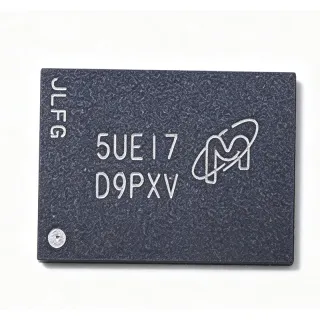
M29W064FB70N3E - 64Mbit 3V NOR Flash 70ns TSOP-48 | Micron
MPN: M29W064FB70N3E ✓ Active| Qty | Unit Price | Extended |
|---|---|---|
| 1 | $0 | $0.00 |
| 10 | $0 | $0.00 |
| 100 | $0 | $0.00 |
| 500 | $0 | $0.00 |
| 1,000 | $0 | $0.00 |
Drop-in alternatives for M29W064FB70N3E — same package, pin-to-pin compatible. Different-package parts requiring PCB rework are excluded.
Quick Comparison Tool — Select alternative parts for side-by-side comparison:
M29W064FB70N3F
✅ Drop-In ⚠️ 参数待验证✓ In Stock
$1.2032 / Unit
View Datasheet →M29W064FT70N3E
✅ Drop-In ⚠️ 参数待验证✓ In Stock
Contact for price
View Datasheet →M29W064FT70N3F
✅ Drop-In ⚠️ 参数待验证✓ In Stock
$6.3 / Unit
View Datasheet →M29W064GB70N3E
✅ Drop-In ⚠️ 参数待验证📋 Reference alternative (not in catalog)
M29W064FB70ZA3SE
✅ Drop-In ⚠️ 参数待验证📋 Reference alternative (not in catalog)
M29W064FB70N3E Maximum Ratings & Electrical Characteristics
| Memory Type | NOR Flash, Parallel |
| Memory Size | 64 Mbit (8M x 8 / 4M x 16) |
| Supply Voltage | 3.0 V to 3.6 V (3V/3.3V) |
| Access Time | 70 ns |
| Interface | Parallel, CFI compliant |
| Boot Block | Bottom boot block (FB variant) |
| Package | 48-Pin TSOP |
| Mounting Type | Surface Mount |
| Operating Temperature | -40C to +125C |
| Organization Switching | Byte/Word selectable via BYTE# pin |
| Reset/Power-Down | RP# pin |
| Data Protection | Block protection, WP# hardware protection |
| Device Signature | Electronic signature for device identification |
| Packaging | Tray |
| RoHS Status | Compliant |
| Brand Source | Micron Technology / Alliance Memory, Inc. (second source) |
| Erase/Program Mode | Word/byte program, block erase, chip erase |
M29W064FB70N3E 48-pin tsop Pin Configuration Guide
Complete pinout information for M29W064FB70N3E (48-pin tsop package). This digital IC includes GPIO, communication interfaces (UART, SPI, I2C), and power pins. Refer to the manufacturer datasheet for alternate pin functions and configuration options. Essential for embedded system design and PCB layout.

No detailed pinout data available for M29W064FB70N3E.
Refer to the datasheet for full pin configuration.
Safe Operating Area (SOA) & Thermal Characteristics
No official SOA curve available for this digital IC. Always operate within absolute maximum ratings specified in the datasheet. Ensure adequate cooling and derate as needed.
Typical Applications
M29W064FB70N3E is suitable for 6 applications: Embedded Boot Code Storage (XIP), Industrial PLC and Automation Controllers, Telecom and Networking Line Cards, Automotive Body and Telematics Modules, Set-Top Boxes and Consumer Video Terminals, Test and Measurement Instruments.
Embedded Boot Code Storage (XIP)
The M29W064FB70N3E is a natural boot-code device for embedded processors because its 70 ns parallel access time supports execute-in-place (XIP) fetching directly from Flash with zero or minimal wait states, eliminating a RAM shadow-copy step at startup. The bottom boot block architecture places protected boot blocks at address 0, matching processors that fetch reset vectors from the bottom of the memory map, and the BYTE# pin lets the same footprint serve 8-bit and 16-bit buses. Block-level hardware protection via WP# prevents accidental corruption of the bootloader during field firmware updates over the remaining blocks.
Recommended
Industrial PLC and Automation Controllers
Industrial programmable logic controllers demand non-volatile firmware storage that survives wide ambient swings and years of continuous power cycling. The M29W064FB70N3E's -40C to +125C operating range covers DIN-rail cabinet environments, while its CFI-compliant command set lets firmware-update code auto-detect geometry and program blocks without device-specific hacks. The 64 Mbit capacity holds both the PLC runtime kernel and application logic, and the RP# pin allows the host to reset the memory bus cleanly after watchdog events, avoiding corrupted reads during brown-out recovery sequences common on factory floors.
Recommended
Telecom and Networking Line Cards
Networking line cards and telecom shelves typically store their boot ROM and configuration images in parallel NOR Flash because deterministic read timing simplifies hardware-based code execution and CRC-checked image validation. The M29W064FB70N3E provides 64 Mbit on a single 3.3 V rail shared with the backplane logic, and its 70 ns access time keeps code-fetch latency low for processor-assisted boot. Block erase/program operations run in-system, enabling remote firmware upgrades across a card fleet, while the electronic signature lets manufacturing test software verify the exact device before burn-in.
Recommended
Automotive Body and Telematics Modules
Mouser lists the M29W064FB70N3E as automotive-rated, and its -40C to +125C range makes it suitable for body control modules, instrument clusters, and telematics boxes that store calibration data and boot firmware. The single 3.0 V to 3.6 V rail integrates cleanly into automotive 5 V and 3.3 V power trees via simple regulation, and hardware block protection secures immobilizer-related boot blocks against accidental writes during cranking transients. Designs should verify the specific qualification grade required by their OEM program and consider the RP# pin for clean reset behavior under load-dump-induced resets.
Recommended
Set-Top Boxes and Consumer Video Terminals
Set-top box platforms historically used parallel NOR Flash for the bootloader because the parallel bus allows the SoC boot ROM to fetch initialization code directly with simple timing controllers. The M29W064FB70N3E's 64 Mbit density holds the bootloader plus a compressed main image, and the 8-bit BYTE# mode reduces bus width requirements on cost-sensitive boards. Its 3 V single supply matches consumer power budgets, while the 70 ns access time supports fast power-on-to-logo times. Field updates rewrite application blocks without touching the hardware-protected boot region, improving recovery reliability.
Recommended
Test and Measurement Instruments
Bench instruments such as oscilloscopes and signal generators store firmware, factory calibration constants, and user settings in non-volatile memory. The M29W064FB70N3E serves as the main firmware store, with the CFI interface simplifying multi-platform firmware builds that must program several Flash geometries from one update utility. The 70 ns access time supports fast POST diagnostics, and block protection isolates the calibration region from firmware rewrites so that a failed update never destroys factory calibration. Its industrial temperature range also covers portable instruments used outdoors or in vehicle-based test setups.
Recommended
Recommended Products Summary
Engineering reference data for M29W064FB70N3E — comparison, design guidance, and compliance information.
Selection Guide
Comparison with Alternatives
| Parameter | This Product | M29W064FB70N3F | M29W064FT70N3E | M29W064FT70N3F | M29W064GB70N3E |
|---|---|---|---|---|---|
| Package | 48-TSOP | 48-TSOP - same | 48-TSOP - same | 48-TSOP - same | 48-TSOP - same |
| Brand | Micron Technology (Alliance Memory second source) | Micron Technology | Micron Technology | Micron Technology | Micron Technology |
| Density | 64 Mbit (8M x 8 / 4M x 16) | 64 Mbit | 64 Mbit | 64 Mbit | 64 Mbit |
| Access Time | 70 ns | 70 ns | 70 ns | 70 ns | 70 ns |
| Supply Voltage | 3.0 V to 3.6 V | 3.0 V to 3.6 V | 3.0 V to 3.6 V | 3.0 V to 3.6 V | 3.0 V to 3.6 V |
| Boot Block Position | Bottom | Bottom | Top | Top | Bottom |
| Operating Temperature | -40C to +125C | -40C to +125C | -40C to +125C | -40C to +125C | -40C to +125C |
| Automotive Rating | Automotive-rated per Mouser listing | [DATA_NEEDED] | [DATA_NEEDED] | [DATA_NEEDED] | [DATA_NEEDED] |
Key Differentiators
- Bottom boot block organization for address-0 boot architectures (vs M29W064FT70N3E)
- Automotive temperature rating in a legacy-friendly parallel interface (vs N25Q064A13ESFA0F)
- Dual second-source supply chain (Micron + Alliance Memory) (vs M29W064FB70N3F)
Design Notes
Drive the RP# (Reset/Power-down) pin with a defined logic level during power-up and brown-out events. If RP# floats during supply transitions, the M29W064FB70N3E can leave an indeterminate state and the host may misread the status register or, in the worst case, initiate a spurious write sequence. Use a supervisor IC or RC network plus pull-up to hold RP# low until VCC is stable, then release it - the device exits reset and becomes read-ready within the datasheet recovery time.
Match bus timing between the processor external memory controller and the 70 ns access window. Derate for capacitive loading: with a heavily loaded 16-bit address/data bus, trace propagation and output buffer delays consume part of the margin, so at bus frequencies above roughly 20 MHz verify address-setup-to-data-valid against the datasheet's output-enable and chip-enable access times, not just the headline 70 ns figure. In BYTE#-low mode remember Q15A becomes A-1 and must be routed as an address line.
Place 0.1 uF ceramic decoupling capacitors at each VCC pin of the 48-TSOP with a solid ground return, since program/erase operations draw transient current pulses that can glitch the supply and disturb other 3.3 V logic on the same rail. Keep the WP# pin driven (tied to VCC when protection is not used, never floating) so that block protection states cannot be altered by noise. Follow the datasheet's program-suspend capability to allow reads of other blocks during firmware updates.
Compliance Information
Distributor listings describe the part as automotive-rated; RoHS compliance is indicated by standard current-production status, but explicit RoHS/REACH/AEC-Q100 certificates were not captured in the verified data snapshot - confirm with Micron or Alliance Memory documentation.