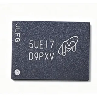
N25Q032A13EF4A0F - 32Mbit SPI NOR Flash 108MHz | Micron
MPN: N25Q032A13EF4A0F ✓ Active| Qty | Unit Price | Extended |
|---|---|---|
| 1 | $1.93 | $1.93 |
| 10 | $1.74 | $17.40 |
| 100 | $1.55 | $155.00 |
| 500 | $1.39 | $695.00 |
| 1,000 | $1.25 | $1,250.00 |
Drop-in alternatives for N25Q032A13EF4A0F — same package, pin-to-pin compatible. Different-package parts requiring PCB rework are excluded.
Quick Comparison Tool — Select alternative parts for side-by-side comparison:
N25Q032A11EF4A0F
✅ Drop-In ⚠️ 参数待验证📋 Reference alternative (not in catalog)
MT25QL032ABB1E12-0SIT
✅ Drop-In ⚠️ 参数待验证📋 Reference alternative (not in catalog)
MT25QU032ABB1E12-0SIT
✅ Drop-In ⚠️ 参数待验证📋 Reference alternative (not in catalog)
W25Q32JVZPIQ
✅ Drop-In📋 Reference alternative (not in catalog)
N25Q032A13EF4A0F Maximum Ratings & Electrical Characteristics
| Memory Type | FLASH - NOR Memory IC (Serial) |
| Memory Size | 32 Mbit (4 MB) |
| Interface | SPI (Multi-I/O) |
| Clock Frequency | 108 MHz |
| Supply Voltage | 3 V (2.7 V to 3.6 V) |
| Package | 8-UFDFPN (MLP8) 4 x 3 mm |
| Mounting Type | Surface Mount |
| Read Modes | Standard, Dual, Quad SPI |
| Erase Granularity | 4 KB subsector / 64 KB sector |
| Grade | Automotive |
| RoHS Status | Compliant |
| Packaging | Tape & Reel (T&R) |
N25Q032A13EF4A0F Pin Configuration
| Pin 1 | S# — Chip select (active low) |
| Pin 2 | DQ1 — Data input/output 1 (dual/quad mode) |
| Pin 3 | W#/VPP — Write protect / write protection voltage |
| Pin 4 | GND — Ground |
| Pin 5 | DQ0 — Data input/output 0 (serial data in/out) |
| Pin 6 | C — Serial clock input |
| Pin 7 | DQ3/HOLD# — Data I/O 3 (quad mode) / Hold control |
| Pin 8 | VCC — Power supply, 2.7 V to 3.6 V |
Safe Operating Area (SOA) & Thermal Characteristics
No official SOA curve available for this digital IC. Always operate within absolute maximum ratings specified in the datasheet. Ensure adequate cooling and derate as needed.
Typical Applications
N25Q032A13EF4A0F is suitable for 6 applications: BIOS / UEFI Boot Storage, FPGA Configuration Storage, Automotive Infotainment and Telematics, Networking and Telecom Equipment, Industrial Automation and PLC Systems, Consumer and IoT Device Code Storage.
BIOS / UEFI Boot Storage
The N25Q032A13EF4A0F is a common choice for BIOS and UEFI firmware storage on x86 embedded, industrial PC, and server-management platforms. Its 32 Mbit density comfortably holds compressed firmware images, while the 108 MHz quad-I/O read path (EBh command) accelerates POST and boot decompression compared with 33 MHz legacy SPI parts. The 4 KB subsector erase granularity allows BIOS option and ME-region updates to be reprogrammed without erasing the whole array, extending usable life. Designers should map the SPI bus at the chipset's supported maximum and add 0.1 uF plus 10 uF decoupling at VCC to absorb program/erase current surges. The automotive-graded A0F unit also suits long-lifecycle industrial motherboards where 7-10 year availability is expected.
Recommended
FPGA Configuration Storage
Xilinx 7-series, Intel/Altera, and Lattice FPGAs frequently boot from a quad-SPI NOR Flash, and the N25Q032A13EF4A0F fits this role directly. The multi-I/O interface supports quad-output (6Bh) and quad-I/O (EBh) reads used by x4 configuration modes, shortening bitstream load time at the 108 MHz clock. 32 Mbit accommodates mid-range bitstreams plus a golden-image second slot for remote-update designs with 4 KB subsector granularity for metadata. A practical layout consideration: pull DQ3/HOLD# up to VCC so the device cannot enter hold state during configuration, and keep S#, C, and DQ traces length-matched and short. The automotive-grade ordering code also supports industrial and transportation FPGA platforms requiring extended-temperature silicon.
Recommended
Automotive Infotainment and Telematics
The A0F automotive program status of the N25Q032A13EF4A0F targets automotive electronics such as infotainment head units, telematics control units, and gateway modules, where it stores bootloader code, calibration parameters, and secure-boot keys. The extended temperature ordering option tolerates under-dash and engine-bay-adjacent environments, and the small 4 x 3 mm UFDFPN package suits dense PCBs. Quad-mode reads at 108 MHz reduce cold-start latency of infotainment SoCs. Engineers should verify PPAP-level documentation with Micron for safety-relevant ECUs, implement block protection on the secure-key sectors, and derate the 2.7-3.6 V supply against automotive load-dump transients with a proper front-end regulator or protection network on the 3.3 V rail.
Recommended
Networking and Telecom Equipment
Routers, switches, and base-station line cards use serial NOR such as the N25Q032A13EF4A0F for boot code, device-tree blobs, and factory calibration data for their main SoCs and CPLDs. The 108 MHz quad read path shortens boot of large embedded Linux images, while 32 Mbit leaves headroom for dual firmware banks with A/B fail-safe updates - the 4 KB subsector architecture allows a small environment-variable partition to coexist with large kernel images. Carrier-grade designs value the automotive-graded silicon for extended temperature tolerance in unventilated rack enclosures. Layout-wise, route the quad SPI bus as a short point-to-point group with series termination (22-33 ohm) on S# and C to control ringing at 108 MHz edges on backplane-adjacent boards.
Recommended
Industrial Automation and PLC Systems
Programmable logic controllers, motor drives, and industrial gateways rely on SPI NOR like the N25Q032A13EF4A0F for firmware retention across power cycles and for storing recipe and diagnostic data. The extended-temperature automotive-grade offering withstands cabinet temperatures commonly specified at -40 C to +85 C and beyond, while the 4 KB subsector erase supports frequent wear-leveled logging of event counters and parameters without disturbing the main firmware image. Quad SPI at 108 MHz reduces the brown-out window during power-fail firmware integrity checks. Designers should implement power-fail-safe write routines (write marker, program, verify, commit) and add bulk capacitance sufficient to finish a 256-byte page program when the 24 V cabinet rail collapses.
Recommended
Consumer and IoT Device Code Storage
Smart-home hubs, IP cameras, set-top boxes, and IoT modules use 32 Mbit SPI NOR such as the N25Q032A13EF4A0F to hold bootloader and radio-stack firmware for Wi-Fi, Zigbee, or NB-IoT SoCs. The small 4 x 3 mm UFDFPN footprint and low pin count fit dense module PCBs, and quad reads at 108 MHz cut boot time for voice-assistant and camera products where instant-on is a selling point. Cost matters in this segment: with unit pricing around $1.93 at qty 1 as of 2026-09-04 and volume tiers near $1.25 at 1000 pieces, it remains price-competitive against cross-brand 32 Mbit parts. The industrial-plus silicon also provides margin for enclosed, passively cooled consumer devices that run hot in service.
Recommended
Recommended Products Summary
Engineering reference data for N25Q032A13EF4A0F — comparison, design guidance, and compliance information.
Selection Guide
Comparison with Alternatives
| Parameter | This Product | N25Q032A11EF4A0F | MT25QL032ABB1E12-0SIT | W25Q32JVZPIQ | W25Q32JVSSIQ |
|---|---|---|---|---|---|
| Package | 8-UFDFPN (MLP8) 4x3 mm | 8-UFDFPN (MLP8) 4x3 mm - same | 8-WSON 4x3 mm - same footprint | 8-WSON 4x3 mm - same footprint | 8-SOIC 208 mil - DIFFERENT footprint |
| Brand | Micron Technology | Micron Technology | Micron Technology | Winbond Electronics | Winbond Electronics |
| Density | 32 Mbit (4 MB) | 32 Mbit | 32 Mbit | 32 Mbit | 32 Mbit |
| Max Clock / Interface | 108 MHz SPI multi-I/O | 108 MHz SPI multi-I/O | 133 MHz-class MT25Q SPI (verify) | 133 MHz quad SPI (W25Q32JV) | 133 MHz quad SPI (W25Q32JV) |
| Supply Voltage | 3 V (2.7 V to 3.6 V) | 2.7 V to 3.6 V | 2.7 V to 3.6 V (QL = 3 V line) | 2.7 V to 3.6 V | 2.7 V to 3.6 V |
| Command Set | Micron N25Q extended SPI | Micron N25Q extended SPI - identical | MT25Q command set (largely compatible) | JEDEC SFDP standard opcodes | JEDEC SFDP standard opcodes |
| Grade / Temperature | Automotive program, extended temp | Industrial temp variant | Industrial, IT grade | Industrial standard (verify grade) | Industrial standard (verify grade) |
| Approx. Price (qty 1) | $1.93 (as of 2026-09-04) | [DATA_NEEDED] | [DATA_NEEDED] | [DATA_NEEDED] | [DATA_NEEDED] |
Key Differentiators
- Automotive program status in a 4x3 mm footprint (vs W25Q32JVZPIQ)
- 108 MHz multi-I/O performance at commodity pricing (vs N25Q032A11EF4A0F)
- Command-set continuity for existing N25Q firmware (vs MT25QL032ABB1E12-0SIT)
- Trade-off: smaller cross-brand ecosystem (vs W25Q32JVSSIQ)
Design Notes
Provide a 10 uF bulk plus 0.1 uF ceramic decoupling pair directly at the VCC pin (pin 8) of the N25Q032A13EF4A0F. Program and erase operations draw burst currents that can sag a shared 3.3 V rail and corrupt a concurrent page program. Estimated: a 256-byte page program with a supply droop budget of 100 mV on a 10 uF capacitor tolerates roughly 1 uA-s of transient charge; size bulk capacitance so the inrush of a 4 KB subsector erase fits within your regulator's transient response. Confirm exact current figures in the manufacturer datasheet ICC tables.
At the 108 MHz clock, treat the SPI bus as a controlled group: keep S#, C, DQ0, DQ1, and DQ3/HOLD# traces short (under ~50 mm) and reference a solid ground plane. Add 22-33 ohm series resistors at the driver on C and S# to damp ringing from stub reflections, and pull DQ3/HOLD# up to VCC with 10 kohm so the device cannot enter hold state during power-up or quad-mode operation. Route W#/VPP with a pull-up as well unless your firmware intentionally manages write protection.
Three recurring pitfalls: (1) Substituting the Winbond W25Q32JV without checking the command set - Micron N25Q opcodes differ from JEDEC SFDP-standard commands, so bootloader drivers may fail silently. (2) Selecting a same-MPN variant in the wrong package outline - the 4x3 mm UFDFPN is footprint-incompatible with 208-mil SOIC-8 and 6x5 mm WSON options; verify the EF4 code. (3) Ignoring block protection on secure-key sectors in automotive designs - program the protection registers during manufacturing test to guard against run-time corruption.
The 8-UFDFPN 4x3 mm package has a small exposed die-attach paddle that is internally tied to GND; connect it to a via-stitched ground fill (at least 3-4 vias) for thermal relief during erase operations and improved noise immunity. Place the part within 30 mm of the host SPI controller to avoid level degradation, and keep flash-under-SoC keepout zones free of switching regulator loops that could couple into the clock line.
Compliance Information
Distributor listings show RoHS compliance. Automotive grade is stated by the Mouser Alliance Memory listing; AEC-Q100 qualification evidence for this exact ordering code should be confirmed directly with Micron. Other compliance fields were not stated in the provided web data.