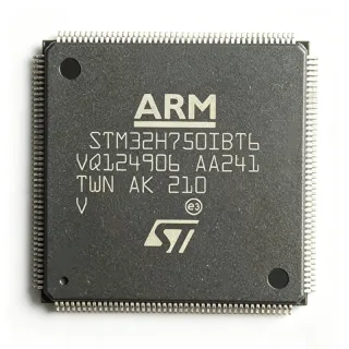
TMS320F2812PGFA - 32-Bit 150MHz C2000 MCU | Texas Instruments
MPN: TMS320F2812PGFA ✓ Active| Qty | Unit Price | Extended |
|---|---|---|
| 1 | $10.24 | $10.24 |
| 10 | $9.6 | $96.00 |
| 100 | $8.9 | $890.00 |
| 500 | $8.2 | $4,100.00 |
| 1,000 | $7.6 | $7,600.00 |
TMS320F2812PGFA Overview
A digital signal controller combines the computational throughput of a digital signal processor with the peripheral integration and ease of use of a microcontroller. Within the semiconductor hierarchy, the TMS320F2812 sits in the C2000 real-time control family of DSP microcontrollers, a product line widely deployed where deterministic interrupt latency and tightly coupled event-driven peripherals matter more than general-purpose application processing.
Key features include the 150 MHz C28x fixed-point CPU core executing from a modified Harvard architecture, 256KB of nonvolatile Flash with in-circuit reprogrammability, dual Event Manager peripherals purpose-built for PWM motor control, and connectivity peripherals including CAN, SCI, and SPI. The Mouser and DigiKey listings confirm the 32-bit 150 MHz fixed-point core with 176-LQFP (24x24 mm) packaging, and the LCSC listing confirms availability with pricing from $10.2303 as of 2026-09-14.
Technically, the C28x core delivers high arithmetic density for control-loop mathematics (PID, Clarke/Park transforms), while the on-chip EMIF allows external SRAM/Flash expansion beyond the internal memory map. The peripheral set is memory-mapped and serviced through a centralized PIE (Peripheral Interrupt Expansion) vectoring scheme that minimizes interrupt service latency, a critical parameter in current-loop applications executing at tens of kilohertz.
Typical applications include industrial motor drives (AC induction, PMSM, BLDC), digital power supplies and solar inverters, and automotive/embedded control systems, where the dual Event Manager PWM blocks and AEC-Q100 heritage make it a proven fit for closed-loop, high-frequency control.
When designing with this device, budget the dual-rail power requirement (1.8V/1.9V core and 3.3V I/O) and place decoupling closely; use the internal PLL with external crystal to reach 150 MHz.
This page synthesizes distributor pricing, verified drop-in alternatives, cross-reference guidance, and practical design notes not found in the manufacturer datasheet.
Drop-in alternatives for TMS320F2812PGFA — same package, pin-to-pin compatible. Different-package parts requiring PCB rework are excluded.
Variants in this series
Same-series models that are drop-in compatible with TMS320F2812PGFA (same form factor and footprint) — differing in Core Processor, Maximum Clock Frequency, Package.
Quick Comparison Tool — Select alternative parts for side-by-side comparison:
TMS320F2812PGFAG4
✅ Drop-In📋 Reference alternative (not in catalog)
TMS320C2812PGFA
✅ Drop-In ⚠️ 参数待验证📋 Reference alternative (not in catalog)
TMS320R2812PGFA
✅ Drop-In ⚠️ 参数待验证📋 Reference alternative (not in catalog)
TMS320F2810PGFA
✅ Drop-In ⚠️ 参数待验证📋 Reference alternative (not in catalog)
TMS320F2812PGFA Maximum Ratings & Electrical Characteristics
| Core Processor | C28x Fixed-Point (C2000) |
| Core Size | 32-Bit |
| Maximum Clock Frequency | 150 MHz |
| Program Memory Type | FLASH |
| Program Memory Size | 256KB (128K x 16) |
| Package | 176-LQFP (24x24 mm) |
| Mounting Type | Surface Mount |
| Peripherals | EMIF, Event Manager (PWM), CAN, SCI, SPI |
| Number of I/O | 56 |
| Series | C2000 C28x Fixed-Point |
| Product Status | Active |
| Packaging | Tray |
TMS320F2812PGFA 176-lqfp (24x24 mm) Pin Configuration Guide
Pin configuration for TMS320F2812PGFA (176-lqfp (24x24 mm) package). This digital IC includes GPIO, communication interfaces (UART, SPI, I2C), and power pins. Refer to the manufacturer datasheet for alternate pin functions and configuration options. Essential for embedded system design and PCB layout.

No detailed pinout data available for TMS320F2812PGFA.
Refer to the datasheet for full pin configuration.
Typical Applications
TMS320F2812PGFA is suitable for 6 applications: Industrial Motor Drives, Digital Power Supplies and Solar Inverters, Automotive Embedded Control, Servo Drives and Robotics, Test and Measurement Instrumentation, Networked Industrial Automation Nodes.
Industrial Motor Drives
The TMS320F2812PGFA is a classic choice for AC induction, PMSM, and BLDC industrial drives. Its dual Event Manager peripherals generate complementary PWM outputs with hardware dead-band insertion, while the 150 MHz C28x fixed-point core executes Clarke/Park transforms and PI current-loop algorithms at tens of kilohertz without core overload. In a typical inverter, the DSP reads phase currents through its ADC, computes the space-vector PWM duty cycles, and outputs six gate signals - all within one PWM period, thanks to the deterministic interrupt architecture. Designers pairing this DSP with isolated gate drivers achieve high-torque, low-ripple motor control proven across a decade of industrial installations.
Recommended
Digital Power Supplies and Solar Inverters
In digitally controlled power converters - photovoltaic inverters, PFC stages, LLC resonant converters - the TMS320F2812PGFA replaces analog control loops with software control law execution at 150 MHz. The C28x core closes voltage and current loops at up to hundreds of kHz sampling rates, implements MPPT algorithms for solar input, and handles grid synchronization. Its EMIF allows adding external SRAM for data logging, and its CAN/SCI interfaces provide supervisory communication. Compared with dedicated analog controllers, the DSP approach enables firmware-updatable control laws, adaptive compensation, and digital diagnostics - key reasons the C2000 family dominates digital-power designs.
Recommended
Automotive Embedded Control
The C2000 series carries AEC-Q100 automotive heritage, and the TMS320F2812 family has shipped in automotive subsystems such as transmission control, electric power steering assist logic, and engine auxiliary actuation. The on-chip CAN peripheral provides the vehicle-network interface, while the Event Manager PWM drives solenoids and small motors with deterministic timing. Its 176-pin LQFP supplies the 56 GPIO needed for sensor and actuation aggregation in body and chassis modules. For new automotive designs, TI recommends the newer C2000 automotive-qualified variants, but the F2812 remains valid for sustaining legacy vehicle platforms and aftermarket controllers.
Recommended
Servo Drives and Robotics
Robotics servo amplifiers demand multi-loop control - current, velocity, and position - executed at high rates with low jitter. The TMS320F2812PGFA's 150 MHz fixed-point core plus dual Event Manager PWM handles three-phase current loops while leaving headroom for encoder processing (incremental or absolute via SPI/QEP) and trajectory interpolation. Deterministic PIE interrupt servicing keeps control-loop phase error stable, which directly improves mechanical smoothness. Its CAN or SCI port links to a host motion controller for command streaming, and the 256KB Flash retains servo tuning parameters and firmware across power cycles without external nonvolatile memory.
Recommended
Test and Measurement Instrumentation
Bench and embedded instrumentation uses the TMS320F2812PGFA as a real-time acquisition and control engine: the EMIF interfaces external high-speed SRAM for sample buffering, the ADC subsystem digitizes sensor channels, and the C28x core applies calibration, filtering, and trigger logic at 150 MHz. SCI and SPI provide host and peripheral connectivity for panel UIs or USB bridge chips. Fixed-point arithmetic is sufficient for RMS computation, digital filtering, and closed-loop source regulation in power analyzers and electronic loads. The 176-LQFP offers the GPIO count needed for range switching, relay control, and front-panel indicators.
Recommended
Networked Industrial Automation Nodes
Factory automation nodes - I/O concentrators, small PLCs, drive front-ends - benefit from the TMS320F2812PGFA's balance of processing throughput and real-time peripherals. The CAN controller links the node to fieldbus networks, SCI/SPI handle local sensors and HMI bridges, and the C28x core runs protocol stacks plus local control logic concurrently under a deterministic scheduler. The EMIF lets designers attach external memory for larger data tables or firmware shadowing, and 56 GPIO directly drive relays, indicators, and discrete sensing lines. Its long field history and stable lifecycle status make it a low-risk choice for multi-year production automation programs.
Recommended
Recommended Products Summary
Engineering reference data for TMS320F2812PGFA — comparison, design guidance, and compliance information.
Selection Guide
Comparison with Alternatives
| Parameter | This Product | TMS320F2812PGFAG4 | TMS320C2812PGFA | TMS320R2812PGFA | TMS320F2810PGFA |
|---|---|---|---|---|---|
| Package | 176-LQFP (24x24 mm) | 176-LQFP (24x24 mm) - same | 176-LQFP (24x24 mm) - same | 176-LQFP (24x24 mm) - same | 176-LQFP (24x24 mm) - same |
| Brand | Texas Instruments | Texas Instruments | Texas Instruments | Texas Instruments | Texas Instruments |
| Core / Clock | C28x 32-bit, 150 MHz | C28x 32-bit, 150 MHz | C28x 32-bit, 150 MHz | C28x 32-bit, 150 MHz | C28x 32-bit, 150 MHz |
| Program Memory | 256KB Flash | 256KB Flash | 256KB ROM | 256KB RAM (volatile) | 128KB Flash |
| EMIF External Memory Interface | Yes | Yes | Yes | Yes (needed for code load) | No |
| Drop-in Compatible | - | Yes - 100% | Yes - pin-to-pin | Yes - pin-to-pin | Yes - pin-to-pin |
| Firmware Impact | None (baseline) | None - identical | ROM requires factory programming | Boot-time code load required | Memory map/EMIF rework if external memory used |
Key Differentiators
- 256KB Flash with EMIF in a single 176-LQFP (vs TMS320F2810PGFA)
- In-circuit reprogrammable Flash (vs TMS320C2812PGFA)
- Nonvolatile memory without boot ROM dependency (vs TMS320R2812PGFA)
Design Notes
The TMS320F2812 uses a dual-rail power architecture (reduced-voltage core rail around 1.8-1.9 V and a 3.3 V I/O rail). TI's power-sequencing guidance for this generation requires attention to core-versus-I/O ramp order to avoid latch-up or I/O cell stress. Estimated: at 150 MHz the core current is on the order of a few hundred milliamperes, so size the core LDO/buck accordingly and add bulk capacitance near the supply pins. Consult the manufacturer datasheet power-supply section for exact tolerances before release.
Place 0.1 uF ceramic decoupling capacitors at every VDDIO/VDD pair plus at least one bulk 10 uF per rail, routed directly to the LQFP power pins. The 176-pin 24x24 mm LQFP keeps all signals on the perimeter, so plan breakout layers before routing: dedicate inner layers to a solid ground plane to minimize loop area for the 150 MHz core switching and the PWM edge rates. Keep crystal and PLL loop components short and isolated from PWM traces to avoid clock jitter in the control loops.
Flash programming on this generation requires the correct wait-state configuration for the 150 MHz clock; code written for 120 MHz-speed versions may mis-time flash reads if wait states are not scaled. Also verify suffix compatibility: the G4 suffix denotes a TI environmental grade of the same silicon, while C2812/R2812 variants use ROM/RAM and cannot be flash-programmed in circuit. Finally, confirm EMIF timing margin if your board depends on external memory, since it is absent on the F2810 variant.
Compliance Information
Environmental compliance must be confirmed per-suffix on the TI product page (ti.com/product/TMS320F2812); the G4 suffix denotes TI's green/lead-free grade per Mouser listing data, but the specific PGFA suffix certificate should be downloaded from TI.