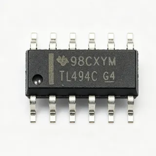
TPS610981 - 3.3V Boost Converter with Integrated LDO | TI
MPN: TPS610981 ✓ Active| Qty | Unit Price | Extended |
|---|---|---|
| 1 | $1.25 | $1.25 |
| 10 | $1.12 | $11.20 |
| 100 | $0.98 | $98.00 |
| 500 | $0.87 | $435.00 |
| 1,000 | $0.76 | $760.00 |
Drop-in alternatives for TPS610981 — same package, pin-to-pin compatible. Different-package parts requiring PCB rework are excluded.
Quick Comparison Tool — Select alternative parts for side-by-side comparison:
TPS610985
✅ Drop-In📋 Reference alternative (not in catalog)
TPS610986
✅ Drop-In📋 Reference alternative (not in catalog)
TPS610987
✅ Drop-In📋 Reference alternative (not in catalog)
TPS610988
✅ Drop-In📋 Reference alternative (not in catalog)
TPS610989
✅ Drop-In📋 Reference alternative (not in catalog)
TPS610990
✅ Drop-In📋 Reference alternative (not in catalog)
TPS610991
✅ Drop-In📋 Reference alternative (not in catalog)
TPS610992
✅ Drop-In📋 Reference alternative (not in catalog)
TPS610981 Maximum Ratings & Electrical Characteristics
| Topology | Boost (Step-Up) with Integrated LDO |
| Number of Outputs | 2 |
| Output Voltage (Boost) | 3.3 V (Fixed) |
| Output Voltage (LDO) | 1.2 V to 3.3 V (Adjustable) |
| Input Voltage Range | 0.7 V to 5.5 V |
| Maximum Output Current (Boost) | 300 mA at 3.3 V from 1.8 V input |
| Quiescent Current | 300 nA (typical) |
| Efficiency | Up to 95% |
| Switching Frequency | [DATA_NEEDED: switching frequency] |
| Package | 6-WSON (1.5x1.5 mm) |
| Operating Temperature Range | -40°C to +85°C |
| Mounting Type | Surface Mount |
| RoHS Status | Compliant |
| Control Scheme | PFM/PWM |
| Protection Features | Over-Temperature, Over-Current |
TPS610981 Pin Configuration
| Pin 1 | SW — Switch pin, connect to inductor |
| Pin 2 | GND — Ground |
| Pin 3 | VIN — Input supply |
| Pin 4 | EN — Enable (active high) |
| Pin 5 | VOUT — Boost output |
| Pin 6 | LDO_OUT — LDO output |
Safe Operating Area (SOA) & Thermal Characteristics
No official SOA curve available for this component. Always operate within absolute maximum ratings specified in the datasheet. Ensure adequate cooling and derate as needed.
Typical Applications
TPS610981 is suitable for 6 applications: Wireless Sensors, Hearing Aids, Portable Medical Devices, IoT Nodes, Wearable Electronics, Battery-Powered Audio Devices.
Wireless Sensors
The TPS610981's ultra-low quiescent current (300 nA) and high efficiency (up to 95%) make it ideal for wireless sensor nodes powered by coin cells or AA batteries. The 3.3V boost rail powers the microcontroller and RF transceiver, while the integrated LDO provides a clean supply for analog sensors. The small 6-WSON package fits compact sensor designs, and the wide input range (0.7V to 5.5V) accommodates battery voltage drop over time. The PFM/PWM control ensures high efficiency across load ranges, extending battery life in duty-cycled applications.
Recommended
Hearing Aids
The TPS610981 is well-suited for hearing aids due to its ultra-low quiescent current and small footprint. The boost converter efficiently steps up a single zinc-air battery (1.4V) to 3.3V for the digital signal processor, while the integrated LDO provides a low-noise supply for the microphone and amplifier. The 300 nA quiescent current is critical for extending battery life in always-on devices. The 6-WSON package (1.5x1.5mm) fits the tiny form factor of modern hearing aids, and the wide input range ensures operation as the battery discharges.
Recommended
Portable Medical Devices
In portable medical devices like glucose monitors and pulse oximeters, the TPS610981 provides a reliable power solution from a single coin cell or small Li-Ion battery. The 3.3V boost rail powers the microcontroller and display, while the LDO output powers sensitive analog front-ends with low noise. The ultra-low quiescent current (300 nA) is essential for devices that remain in standby for long periods. The device's small package and high efficiency (up to 95%) help minimize device size and maximize battery life, meeting the stringent power requirements of medical wearables.
Recommended
IoT Nodes
The TPS610981 is ideal for IoT nodes that require long battery life and compact size. Its ultra-low quiescent current (300 nA) minimizes standby power, while the boost converter efficiently steps up battery voltage to 3.3V for sensors, MCUs, and wireless modules. The integrated LDO provides a clean supply for analog sensors, reducing noise. The wide input voltage range (0.7V to 5.5V) supports various battery chemistries, and the small 6-WSON package enables miniaturized designs. The PFM/PWM control ensures high efficiency across load ranges, making it suitable for duty-cycled IoT applications.
Recommended
Wearable Electronics
The TPS610981 is perfect for wearable devices like smartwatches and fitness trackers, where space and battery life are critical. The compact 6-WSON package (1.5x1.5mm) fits into tight PCB layouts, and the ultra-low quiescent current (300 nA) extends battery life. The boost converter provides a stable 3.3V rail for the main processor and display, while the integrated LDO powers low-noise analog circuits such as heart-rate sensors. The wide input range supports various battery types, and the high efficiency (up to 95%) minimizes power loss, making it an excellent choice for energy-constrained wearables.
Recommended
Battery-Powered Audio Devices
The TPS610981 is suitable for battery-powered audio devices such as portable speakers and voice recorders. The boost converter provides a 3.3V rail for the audio codec and amplifier, while the integrated LDO supplies a low-noise rail for analog audio circuits, reducing audible noise. The ultra-low quiescent current (300 nA) is beneficial for standby mode, preserving battery life. The small package and high efficiency (up to 95%) make it ideal for compact, portable audio products. The wide input range accommodates various battery configurations, ensuring reliable operation.
Recommended
Recommended Products Summary
Engineering reference data for TPS610981 — comparison, design guidance, and compliance information.
Selection Guide
Comparison with Alternatives
| Parameter | This Product | TPS610985 | TPS610986 | TPS610987 |
|---|---|---|---|---|
| Package | 6-WSON (1.5x1.5) | 6-WSON (1.5x1.5) | 6-WSON (1.5x1.5) | 6-WSON (1.5x1.5) |
| Brand | Texas Instruments | Texas Instruments | Texas Instruments | Texas Instruments |
| Output Voltage (Boost) | 3.3V | [DATA_NEEDED] | [DATA_NEEDED] | [DATA_NEEDED] |
| Quiescent Current | 300 nA | [DATA_NEEDED] | [DATA_NEEDED] | [DATA_NEEDED] |
| Max Output Current | 300 mA | [DATA_NEEDED] | [DATA_NEEDED] | [DATA_NEEDED] |
| Input Voltage Range | 0.7V to 5.5V | [DATA_NEEDED] | [DATA_NEEDED] | [DATA_NEEDED] |
| Integrated LDO | Yes | Yes | Yes | Yes |
| Efficiency | Up to 95% | [DATA_NEEDED] | [DATA_NEEDED] | [DATA_NEEDED] |
Key Differentiators
- Ultra-low quiescent current of 300 nA (vs TPS610985)
- Integrated LDO provides a second output rail (vs TPS610985)
- Wide input voltage range from 0.7V to 5.5V (vs TPS610985)
Design Notes
Place the input and output capacitors as close to the IC pins as possible to minimize parasitic inductance and ensure stable operation. Use a 2.2 µH inductor with low DCR for high efficiency. The inductor should be placed near the SW pin to reduce switching noise. Follow the layout guidelines in the datasheet for optimal performance.
The TPS610981's ultra-low quiescent current (300 nA) is achieved through PFM control at light loads. For applications with varying load, ensure the transition between PFM and PWM does not cause output voltage ripple. Use appropriate output capacitance to maintain stability during load transients.
Although the TPS610981 is a small package, it can dissipate significant power at high output currents. Ensure adequate copper area on the PCB for heat dissipation. The thermal resistance of the 6-WSON package should be considered in high-temperature environments. Refer to the datasheet for thermal performance guidelines.
Compliance Information
RoHS compliant per TI product page. Other compliance data not specified in provided data.