Supervisors & Reset
Products (7)
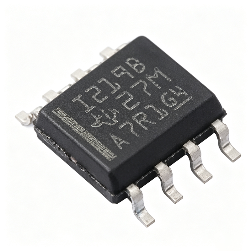
INA219BIDR - 26V 12-Bit I2C Power Monitor | Texas Instruments
The Texas Instruments INA219BIDR is a high-side bidirectional current shunt and power monitor with an I2C- or SMBUS-compatible interface. It senses bus voltages from 0 to 26 V and reports current, voltage, and power through a 12-bit ADC. The device operates from a single 3.0 V to 5.5 V supply and is available in an 8-pin SOIC package. With a maximum accuracy of 0.5% over temperature (INA219B grade), it provides precise monitoring for a wide range of applications. A current shunt monitor is an integrated circuit that measures the voltage drop across a sense resistor placed in series with a load, converting this small differential voltage into a proportional output. The INA219BIDR is a digital power monitor, a subtype of current shunt monitor that includes an ADC and digital interface to report current, voltage, and power directly to a microcontroller. This places it in the hierarchy: current shunt monitor -> power monitor -> analog front-end -> signal chain IC. Key features include 16 programmable I2C addresses, programmable conversion times and filtering, and a calibration register that enables direct readouts of current in amperes. The device also includes an internal multiplier for power calculation, reducing host processor overhead. The INA219BIDR is specified for operation from -40C to +125C, making it suitable for industrial and automotive environments. The INA219BIDR uses a zero-drift architecture to minimize input offset voltage and drift, ensuring accurate measurements over temperature and time. The 12-bit ADC provides a resolution of 10 uV per LSB on the shunt voltage channel, allowing precise current sensing with minimal shunt resistance. The I2C interface supports standard (100 kHz), fast (400 kHz), and high-speed modes, enabling flexible integration into various system architectures. Typical applications include power management in servers, telecom equipment, battery chargers, and power supplies. The device is also used in test and measurement instruments, industrial automation, and consumer electronics where accurate power monitoring is critical. Its high-side sensing capability allows it to monitor current without disturbing the ground path, making it ideal for systems with shared grounds. When designing with the INA219BIDR, ensure the shunt resistor is placed in the high-side path and the bus voltage is within the 0-26 V range. The address pins allow up to 16 devices on the same bus, and the ALERT pin can be configured to signal overcurrent or undervoltage conditions. Proper decoupling on the supply pin and careful PCB layout are essential for optimal performance.
LM94 - Hardware Monitor with PI Loop Fan Control | Texas Instruments
The LM94 is a hardware monitor IC from Texas Instruments (originally National Semiconductor) designed for server and computer system management. It features a two-wire digital interface compatible with SMBus 2.0, enabling communication with a host controller for real-time monitoring and control. Using a Sigma-Delta ADC, the LM94 measures the temperature of four remote diode-connected transistors as well as its own die temperature, and it also monitors 16 power supply voltages. This comprehensive monitoring capability makes it ideal for advanced thermal and power management in servers, workstations, and networking equipment. A hardware monitor is a specialized IC that combines temperature sensing, voltage monitoring, and fan control into a single device, typically used in computing systems to ensure reliable operation and prevent overheating. It sits within the broader category of system management ICs, which are essential for data center and enterprise computing infrastructure. The LM94's integration of multiple monitoring functions reduces board space and simplifies design compared to discrete solutions. Key features of the LM94 include its TruTherm technology, which supports precision thermal diode measurements of processors built on sub-micron processes, improving accuracy for modern CPUs. The device also incorporates a PI (Proportional-Integral) loop fan control algorithm, allowing automatic fan speed adjustment based on temperature readings to optimize cooling efficiency and reduce acoustic noise. The 16 voltage monitors cover critical rails such as Vcore, memory, and I/O supplies, providing comprehensive power integrity oversight. Technically, the LM94 uses a Sigma-Delta ADC for high-resolution temperature and voltage measurements, ensuring accurate data for system management. The SMBus 2.0 interface supports standard and fast modes, with programmable alert thresholds for out-of-range conditions. The device operates from a 3.3V supply and is available in a 44-pin TSSOP package, offering a compact footprint for space-constrained designs. Typical applications include server motherboards, blade servers, storage systems, and network switches, where the LM94 provides essential thermal and power monitoring. Its PI loop fan control is particularly valuable in high-density computing environments where efficient cooling is critical. The device's ability to monitor multiple remote diodes makes it suitable for multi-core processors and other heat-generating components. When designing with the LM94, ensure proper PCB layout for the remote diode connections to minimize noise and maintain measurement accuracy. The SMBus address is set via external pins, allowing multiple devices on the same bus. Consider the thermal characteristics of the package and provide adequate airflow for reliable operation.
LTC2928CUHF#PBF - 4-Channel Power Sequencer & Supervisor | ADI
The LTC2928CUHF#PBF from Analog Devices is a four-channel cascadable power supply sequencer and high accuracy supervisor. It is designed to manage the power-up and power-down sequencing of multiple supply rails in complex electronic systems, ensuring that each rail turns on and off in a controlled order to prevent latch-up, excessive current draw, or damage to sensitive ICs. The device is housed in a 38-pin QFN package (5x7 mm) and operates over a wide supply voltage range, making it suitable for a variety of industrial, networking, and computing applications. A power supply sequencer is a specialized power management IC that controls the order and timing of multiple voltage rails during system startup and shutdown. It is a critical component in systems with multiple supply voltages, such as FPGAs, ASICs, processors, and mixed-signal boards, where improper sequencing can lead to functional failures or permanent damage. The LTC2928 integrates sequencing and supervision into a single device, reducing board space and component count compared to discrete solutions. Key features of the LTC2928 include the ability to sequence up to four supplies per device, with cascading capability to handle an unlimited number of supplies by connecting multiple LTC2928s together. Sequencing thresholds, order, and timing are configured with just a few external resistors and capacitors, eliminating the need for software or PC board layout changes during development. The device also provides high-accuracy supervision with over-voltage and fault indication, selectable system shutdown, and fault event reporting with diagnostics. Technically, the LTC2928 uses a resistor-programmable architecture to set the sequencing order and timing, with an internal precision reference for accurate threshold detection. It supports both positive and negative supply monitoring, and its cascading interface allows seamless expansion. The device operates from a single supply voltage, typically 3.3V or 5V, and includes an open-drain fault output for system-level monitoring. Typical applications include FPGA and ASIC power sequencing, server and storage systems, telecom and networking equipment, and industrial control systems. The LTC2928 is particularly suited for designs where multiple voltage rails must be sequenced reliably without software intervention, and where high accuracy supervision is required to protect downstream components. When designing with the LTC2928, it is important to properly set the sequencing thresholds and timing using external resistors and capacitors, and to ensure adequate decoupling on the supply pins. The device's cascading feature should be used for systems with more than four rails, and the fault output should be connected to a system controller for proper fault handling.
TPS1689 - 9V-80V, 20A Stackable eFuse with PMBus | TI
The Texas Instruments TPS1689 is a stackable integrated hot-swap eFuse (electronic fuse) with PMBus digital telemetry, providing high-current circuit protection and power management. It operates from a 9V to 80V input range with a 92V absolute maximum rating, integrates a low on-resistance FET of 3.5mOhm (typ), and supports up to 20A of continuous current. An eFuse is an electronic circuit protection device that guards against overloads, short circuits, and excessive inrush current. Unlike traditional fuses, eFuses are resettable and offer programmable current limits, making them essential for hot-swap applications where boards are inserted into live backplanes. The TPS1689 belongs to the hot-swap controller / circuit protection family within the broader power management IC hierarchy. Key features include a PMBus interface for telemetry, control, and configuration, enabling real-time monitoring of current, voltage, and temperature. The device supports stackable operation, allowing multiple eFuses to be paralleled for higher current capability, and the IMON pins of multiple TPS1689x or TPS1685x devices can be tied together to report total current in parallel configurations. Multiple protection modes cover overcurrent, overvoltage, undervoltage, and thermal shutdown. The output withstands negative transient voltages up to -5V. Technically, the integrated 3.5mOhm power FET minimizes conduction losses and voltage drop at high currents, while PMBus-programmable current limits, slew rates, and fault responses give designers flexibility. Digital telemetry supports system-level health monitoring, improving reliability and efficiency in power distribution trees. Typical applications include 48V backplane hot-swap power, server and datacenter power distribution, telecom equipment, and industrial automation. The wide 9V-80V input range fits 48V rails with transient headroom. Design with the TPS1689 requires attention to thermal management: PCB copper area and thermal vias are essential at 20A loads. Configure PMBus registers carefully so current-limit and fault-response settings match the application.

TPS23521 - -10V to -80V Hot Swap Controller | Texas Instruments
The Texas Instruments TPS23521 is a high-performance hot swap controller for -10V to -80V telecom power systems, integrating dual current limit and dual gate drive in a 16-pin TSSOP (PWT) package. It enables safe board insertion and removal from live -48V backplanes, serving network routers, switches, and other high-power telecom equipment. A hot swap controller is a power management IC that safely connects and disconnects a load from a live power bus, limiting inrush current and preventing connector arcing and system glitches. It works with an external pass MOSFET, current sensing, and gate control, and belongs to the broader power management IC hierarchy alongside e-fuses and hot swap controllers. Key features include a 200V absolute maximum rating for survivability during lightning surge tests per IEC61000-4-5, dual current limit with dual gate drive for independent control of two MOSFETs, and a soft start capacitor disconnect function that enables soft start at power-up while improving transient response in normal operation. The device operates over -40C to +85C and is RoHS compliant. The TPS23521 uses a proprietary architecture providing precise current sensing and fast response to overcurrent faults. Its high-voltage capability and robust design make it well suited for harsh telecom environments with -48V battery plants, where input transients from lightning surge and hot swapping are common design challenges. Typical applications include -48V hot swap in telecom rectifiers, network routers, Ethernet switches, and base station power distribution. With appropriate external MOSFETs, the dual gate drive supports high-current designs up to several hundred amps. Design tip: choose the soft start capacitor to limit inrush current to safe MOSFET SOA levels, and provide low-inductance, thermally adequate PCB paths for the external pass devices. Pricing varies by package suffix and quantity; refer to authorized distributors for current stock and pricing as of 2026-08-29.

TPS3711 - 36V Voltage Detector | Texas Instruments | SOT-23-6
The Texas Instruments TPS3711 is a precision voltage detector that combines a comparator and an internal 400 mV reference for undervoltage detection. It operates over a wide supply voltage range of 1.8 V to 36 V, making it suitable for a variety of industrial and automotive applications. The device features a high-accuracy threshold voltage of 400 mV with 0.75% accuracy over temperature and built-in hysteresis for noise rejection, ensuring stable output operation without false triggering. The TPS3711 is available in a SOT-23-6 (also referred to as SOT-6) package and is specified over the junction temperature range of -40°C to +125°C. A voltage detector, also known as a voltage supervisor or reset IC, is a component that monitors a supply voltage and asserts a signal when the voltage falls below a predetermined threshold. It is a type of supervisory circuit within the broader category of power management ICs. Voltage detectors are essential in microprocessor systems, where they ensure that the processor is held in reset until the supply voltage is stable, preventing erratic operation during power-up and brown-out conditions. Key features of the TPS3711 include an open-drain output rated to 25 V, which allows for flexible interfacing with various logic levels and loads. The built-in hysteresis provides noise immunity, and the wide supply range accommodates both low-voltage and high-voltage rails. The device's low quiescent current makes it suitable for battery-powered applications. Technically, the TPS3711 uses a precision bandgap reference and a comparator to detect undervoltage conditions. The threshold is set by an external resistor divider connected to the sense pin, allowing for adjustable trip points. The open-drain output requires an external pull-up resistor, and the output can be used to drive a reset input of a microcontroller or to gate a power supply. Typical applications include undervoltage detection in industrial control systems, automotive electronics, and portable devices. The wide input range makes it ideal for monitoring 12V, 24V, and 36V rails. The device's small SOT-23-6 package is space-efficient for compact PCB designs. When designing with the TPS3711, ensure that the external resistor divider is properly sized to set the desired threshold voltage, and consider the hysteresis to avoid chattering. The open-drain output should be pulled up to the appropriate logic voltage, and the input should be decoupled with a capacitor to filter noise.

UCD9090 - 10-Rail Power Sequencer & Monitor | Texas Instruments
The Texas Instruments UCD9090 is a 10-rail PMBus/I2C addressable power-supply sequencer and monitor. It integrates a 12-bit ADC for monitoring up to 10 power-supply voltage inputs, and 23 GPIO pins can be used for power-supply enables, power-on reset signals, external interrupts, cascading, or other system functions. Ten of these pins offer PWM functionality, enabling flexible control of power rails. The device is available in a 48-pin VQFN (7x7) package, suitable for compact board designs. A power-supply sequencer and monitor is a specialized power management IC that controls the order in which multiple voltage rails are turned on and off during system startup and shutdown. This is critical in complex electronic systems where certain rails must be established before others to prevent latch-up, excessive current draw, or damage to sensitive components. The UCD9090 sits within the power management IC hierarchy, specifically under the category of sequencers and monitors, which are essential for reliable multi-rail power delivery in servers, networking equipment, and industrial systems. Key features of the UCD9090 include its 10-channel sequencing capability, 12-bit ADC for accurate voltage monitoring, and PMBus/I2C interface for configuration and telemetry. The device supports ACPI (Advanced Configuration and Power Interface) for advanced power management in computing systems. Its GPIO pins provide versatile control options, including PWM outputs for margining or dynamic voltage scaling. The UCD9090 is designed for high-reliability applications, with a wide operating temperature range and robust fault handling. Technically, the UCD9090 uses a digital state machine to manage sequencing sequences, which can be programmed via PMBus commands. The integrated ADC samples each rail's voltage and compares it against programmable thresholds, triggering faults if voltages exceed or fall below limits. The device can also log fault events and report them to a host controller. This architecture enables precise, repeatable power sequencing and monitoring, reducing the need for external supervisory circuits. Typical applications include server and storage systems, networking equipment, telecommunications infrastructure, and industrial control systems. In these applications, the UCD9090 ensures that power rails are sequenced correctly, preventing system failures and improving reliability. Its PMBus interface allows for real-time monitoring and control, making it ideal for systems that require dynamic power management. When designing with the UCD9090, it is important to configure the sequencing parameters and fault thresholds via PMBus to match the specific power-up requirements of the system. Proper decoupling and layout are essential to ensure accurate ADC readings and stable operation. The device's flexibility in GPIO assignment should be leveraged to optimize board layout and minimize signal routing complexity.