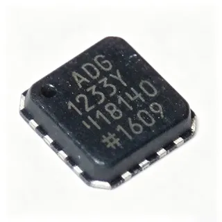
AD9751ASTZ - 10-Bit 300 MSPS TxDAC+ DAC | Analog Devices
MPN: AD9751ASTZ ✓ Active| Qty | Unit Price | Extended |
|---|---|---|
| 1 | $44.59 | $44.59 |
| 10 | $41.23 | $412.30 |
| 100 | $36.87 | $3,687.00 |
| 500 | $33.45 | $16,725.00 |
| 1,000 | $30.12 | $30,120.00 |
Drop-in alternatives for AD9751ASTZ — same package, pin-to-pin compatible. Different-package parts requiring PCB rework are excluded.
Quick Comparison Tool — Select alternative parts for side-by-side comparison:
AD9751ASTZRL
✅ Drop-In✓ In Stock
$11.75 / Unit
View Datasheet →AD9751AST
✅ Drop-In📋 Reference alternative (not in catalog)
AD9751ASTZRL
✅ Drop-In✓ In Stock
$11.75 / Unit
View Datasheet →AD9751ASTZ
✅ Drop-In✓ In Stock
$30.12 / Unit
View Datasheet →AD9751ASTZRL
✅ Drop-In✓ In Stock
$11.75 / Unit
View Datasheet →AD9751ASTZ Maximum Ratings & Electrical Characteristics
| Resolution | 10 bit |
| Maximum Update Rate | 300 MSPS |
| Number of Channels | 1 |
| Supply Voltage Range | 3.0 V to 3.6 V |
| Full-Scale Output Current | 20 mA |
| SFDR (at 10 MHz output) | 68 dBc |
| Glitch Energy | 5 pV-s |
| Package | 48-LQFP (7x7 mm) |
| Operating Temperature Range | -40C to +85C |
| Interface Type | Parallel |
| Input Format | Binary or Two's Complement |
| Power Dissipation | [DATA_NEEDED: Power Dissipation] |
| RoHS Status | Compliant |
| Mounting Type | Surface Mount |
| Output Type | Current - Differential |
AD9751ASTZ Pin Configuration
| Pin 1 | CLK — Clock input, rising edge latches data |
| Pin 2 | GND — Ground |
| Pin 3 | DB0 — Data bit 0 (LSB) |
| Pin 4 | DB1 — Data bit 1 |
| Pin 5 | DB2 — Data bit 2 |
| Pin 6 | DB3 — Data bit 3 |
| Pin 7 | DB4 — Data bit 4 |
| Pin 8 | DB5 — Data bit 5 |
| Pin 9 | DB6 — Data bit 6 |
| Pin 10 | DB7 — Data bit 7 |
| Pin 11 | DB8 — Data bit 8 |
| Pin 12 | DB9 — Data bit 9 (MSB) |
| Pin 13 | AVDD — Analog power supply |
| Pin 14 | AVDD — Analog power supply |
| Pin 15 | IOUT — Differential current output (positive) |
| Pin 16 | IOUTB — Differential current output (negative) |
| Pin 17 | GND — Ground |
| Pin 18 | GND — Ground |
| Pin 19 | DVDD — Digital power supply |
| Pin 20 | DVDD — Digital power supply |
| Pin 21 | MODE — Input format select (binary/two's complement) |
| Pin 22 | PWRDN — Power down control |
| Pin 23 | GND — Ground |
| Pin 24 | GND — Ground |
Safe Operating Area (SOA) & Thermal Characteristics
No official SOA curve available for this component. Always operate within absolute maximum ratings specified in the datasheet. Ensure adequate cooling and derate as needed.
Typical Applications
AD9751ASTZ is suitable for 6 applications: Base Station Transmit Path, Arbitrary Waveform Generator, Direct Digital Synthesis (DDS), Communications Test Equipment, Radar and Electronic Warfare, Medical Ultrasound Imaging.
Base Station Transmit Path
The AD9751ASTZ is ideal for base station transmit paths where high-speed digital-to-analog conversion is required. Its 300 MSPS update rate and 10-bit resolution enable the generation of wideband IF signals with good spectral purity. The dual muxed port interface simplifies interfacing with digital baseband processors, allowing interleaved data input to achieve high throughput. The device's SFDR of 68 dBc at 10 MHz ensures minimal spurious emissions, which is critical for meeting communication standards. The integrated voltage reference reduces external component count, and the 3.0-3.6V supply is compatible with modern FPGA and ASIC I/O levels. In a typical application, the AD9751 converts digital baseband samples to an analog IF signal, which is then upconverted to RF. The differential current output can be directly connected to a transformer or balun for single-ended conversion. Proper layout and decoupling are essential to maintain signal integrity at these speeds.
Recommended
Arbitrary Waveform Generator
In arbitrary waveform generators (AWGs), the AD9751ASTZ provides the high-speed DAC core necessary for generating complex waveforms. With a 300 MSPS update rate, it can produce signals up to 150 MHz (Nyquist frequency) with good fidelity. The 10-bit resolution offers 1024 amplitude levels, suitable for many test and measurement applications. The dual muxed port allows the AWG to accept data from two memory banks, enabling seamless waveform sequencing. The device's low glitch energy (5 pV-s) minimizes transient errors, ensuring clean output transitions. The differential current output can be converted to a voltage using an external resistor or transformer, providing flexibility in output stage design. The integrated voltage reference simplifies calibration. For high-speed AWGs, the AD9751's performance is a key enabler for applications such as radar testing, communications signal simulation, and biomedical waveform generation.
Recommended
Direct Digital Synthesis (DDS)
The AD9751ASTZ is well-suited for direct digital synthesis (DDS) systems, where it converts digitally synthesized sine waves into analog signals. Its high update rate of 300 MSPS allows the generation of frequencies up to 150 MHz, making it suitable for frequency-agile signal sources. The 10-bit resolution provides adequate spurious performance for many applications, with an SFDR of 68 dBc at 10 MHz. The dual muxed port interface can be used to interleave data from a DDS engine, effectively doubling the data throughput. The device's fast settling time and low glitch energy ensure accurate waveform reproduction. In a DDS system, the AD9751 is typically driven by a high-speed digital ASIC or FPGA that generates the phase and amplitude data. The differential current output can be terminated with a resistor to produce a voltage, or fed into a reconstruction filter. The integrated voltage reference reduces external components, and the 3.0-3.6V supply is compatible with digital logic.
Recommended
Communications Test Equipment
The AD9751ASTZ is used in communications test equipment such as signal generators and channel emulators. Its high update rate and good SFDR make it suitable for generating clean test signals for evaluating receivers and transmitters. The 10-bit resolution is adequate for many test scenarios, and the dual muxed port allows for flexible data input. The device's wide operating temperature range (-40C to +85C) ensures reliable operation in various environments. In a signal generator, the AD9751 converts digital waveform data into analog signals that can be modulated and shaped. The differential current output can be converted to a single-ended voltage using a transformer, which is then amplified and filtered. The integrated voltage reference simplifies calibration, and the low glitch energy minimizes transient errors. The compact 48-LQFP package is suitable for benchtop instruments where space is at a premium.
Recommended
Radar and Electronic Warfare
In radar and electronic warfare systems, the AD9751ASTZ is used for generating wideband waveforms for target simulation and jamming. Its 300 MSPS update rate enables the generation of chirp signals and other complex modulations. The 10-bit resolution provides sufficient dynamic range for many applications, and the SFDR of 68 dBc ensures low spurious emissions. The dual muxed port interface allows for high-speed data input from digital signal processors. The device's rugged design and wide temperature range make it suitable for military environments. In a radar target simulator, the AD9751 converts digital waveform data into analog signals that are upconverted to RF and transmitted. The differential current output can be matched to a 50-ohm system using a transformer. The integrated voltage reference reduces component count, and the low glitch energy ensures clean waveform generation. The compact package is ideal for space-constrained defense electronics.
Recommended
Medical Ultrasound Imaging
The AD9751ASTZ can be used in medical ultrasound imaging systems for generating transmit waveforms. Its high update rate allows the generation of high-frequency ultrasound pulses, and the 10-bit resolution provides good amplitude control. The dual muxed port interface can handle the high data rates required for array transducers. The device's low power consumption is beneficial for portable ultrasound devices. In an ultrasound system, the AD9751 converts digital waveform data into analog signals that drive the transducer elements. The differential current output can be converted to a voltage and amplified to the required level. The integrated voltage reference simplifies design, and the compact package is suitable for handheld devices. The wide operating temperature range ensures reliable operation in clinical environments. The SFDR performance helps minimize artifacts in the ultrasound image.
Recommended
Recommended Products Summary
Engineering reference data for AD9751ASTZ — comparison, design guidance, and compliance information.
Selection Guide
Comparison with Alternatives
| Parameter | This Product | AD9751ASTZRL | AD9751AST | AD9751ASTZRL |
|---|---|---|---|---|
| Package | 48-LQFP (7x7 mm) | 48-LQFP (7x7 mm) - same | 48-LQFP (7x7 mm) - same | 48-LQFP (7x7 mm) - same |
| Brand | Analog Devices | Analog Devices | Analog Devices | Analog Devices |
| Resolution | 10 bit | 10 bit | 10 bit | 10 bit |
| Maximum Update Rate | 300 MSPS | 300 MSPS | 300 MSPS | 300 MSPS |
| Supply Voltage Range | 3.0V to 3.6V | 3.0V to 3.6V | 3.0V to 3.6V | 3.0V to 3.6V |
| Full-Scale Output Current | 20 mA | 20 mA | 20 mA | 20 mA |
| SFDR (at 10 MHz) | 68 dBc | 68 dBc | 68 dBc | 68 dBc |
| RoHS Compliant | Yes | Yes | No | Yes |
Key Differentiators
- Dual muxed port interface (vs AD9751AST)
- RoHS compliance (vs AD9751AST)
- Tape-and-reel packaging option (vs AD9751ASTZ (tray))
Design Notes
Decouple the AVDD and DVDD pins with 0.1uF ceramic capacitors placed as close to the pins as possible. Additionally, use a 10uF bulk capacitor on each supply rail. The analog and digital supplies should be separated to minimize noise coupling. A ferrite bead can be used between the analog and digital supply rails to further isolate them.
For optimal performance, use a solid ground plane and avoid splitting it under the DAC. Route the differential output traces (IOUT and IOUTB) with equal length and impedance to maintain balance. Keep the clock input trace short and terminated to minimize reflections. Use 50-ohm controlled impedance for the clock and data lines if possible.
Ensure the clock source has low jitter to achieve the specified SFDR. A jittery clock can degrade the dynamic performance. Also, do not exceed the absolute maximum ratings for supply voltage and output current. The output current should be terminated with a 50-ohm load or transformer to avoid saturation. Verify the input data setup and hold times to ensure proper latching.
Compliance Information
RoHS compliant per distributor listings. No AEC-Q100 qualification for this part.