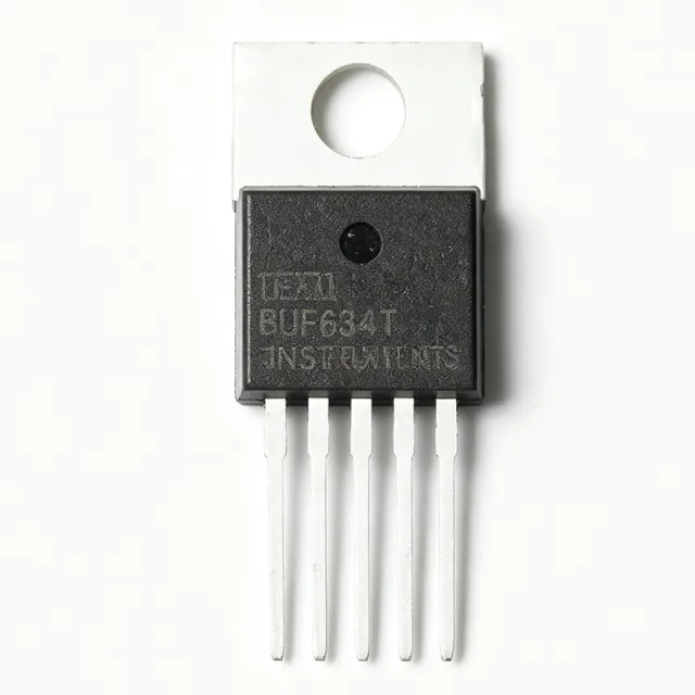
BUF634T - 250mA High-Speed Buffer, 2000V/us | Texas Instruments
MPN: BUF634T ✓ Active| Qty | Unit Price | Extended |
|---|---|---|
| 1 | $13.17 | $13.17 |
| 10 | $12.6 | $126.00 |
| 100 | $11.5 | $1,150.00 |
| 500 | $10.2 | $5,100.00 |
| 1,000 | $9.4 | $9,400.00 |
BUF634T Overview
A buffer amplifier (also called a unity-gain voltage follower) is a specialized amplifier stage with a gain of one that isolates a high-impedance source from a low-impedance load. In the signal-chain hierarchy, buffers sit between operational amplifiers and their loads: an op amp provides voltage gain while the buffer provides current gain, preventing load-induced distortion and thermal feedback inside the gain element. Buffers are a core building block of analog power management and output driver design.
Key features of the BUF634T include 250 mA of continuous output current, an extremely fast 2000 V/us slew rate, and a unique pin-selected bandwidth mode: connecting the BW pin to V- enables the full 180 MHz bandwidth (1.5 mA typical quiescent... 30 MHz mode draws only 1.5 mA... full 180 MHz mode draws approximately 11 mA). Internal current limiting and thermal shutdown protection provide robustness against output shorts and overloads. The device is fabricated on a bipolar process optimized for speed and drive capability rather than precision offset.
Architecturally, the BUF634 is a completely open-loop, unity-gain buffer, so it adds no phase shift from feedback compensation and can be placed inside an op amp feedback loop to boost output current, eliminate thermal feedback errors in the op amp input stage, and improve capacitive load drive without oscillation risk.
Typical applications include headphone amplifier output stages (a classic pairing with the OPA627 or OPA134), video distribution and line driving, op amp output current boosting for test and measurement instrumentation, and capacitive load isolation for ADC input drivers and cable drivers.
Design consideration: the BUF634T is not a precision amplifier - offset voltage and drift are far looser than a precision op amp, so place it inside an overall feedback loop when DC accuracy matters. Power dissipation scales with load current and supply headroom, so the TO-220-5 tab should be heat-sunk for sustained high-current operation.
This page synthesizes distributor pricing, drop-in alternative analysis, and practical design notes not found in the manufacturer datasheet.
Drop-in alternatives for BUF634T — same package, pin-to-pin compatible. Different-package parts requiring PCB rework are excluded.
Variants in this series
Same-series models that are drop-in compatible with BUF634T (same form factor and footprint) — differing in Function, Package, Supply Voltage Range.
Quick Comparison Tool — Select alternative parts for side-by-side comparison:
BUF634AIDDAR
✓ In Stock
$2.15 / Unit
View Datasheet →BUF634T Maximum Ratings & Electrical Characteristics
| Function | Unity-gain high-speed buffer amplifier |
| Number of Circuits | 1 |
| Output Current | 250 mA |
| Slew Rate | 2000 V/us |
| Bandwidth | 180 MHz (pin-selected); 30 MHz low-power mode |
| Quiescent Current | 1.5 mA (30 MHz BW mode) |
| Supply Voltage Range | Up to +/-18 V |
| Input Type | Bipolar |
| Protection Features | Internal current limit, thermal shutdown |
| Topology | Open-loop buffer (usable inside op amp feedback loop) |
| Package | TO-220-5 |
| Mounting Type | Through Hole |
| RoHS Status | Compliant |
| Upgraded Version | BUF634A (higher slew rate 3750 V/us, 210 MHz BW) |
BUF634T Pin Configuration
| Pin 1 | V+ — Positive power supply |
| Pin 2 | IN — Buffer input |
| Pin 3 | OUT — Buffer output (250 mA capability) |
| Pin 4 | V- — Negative power supply; metal tab connects here for heatsinking |
| Pin 5 | BW — Bandwidth select: tie to V- for 30 MHz low-power mode (1.5 mA); full bias for 180 MHz mode |
Typical Applications
BUF634T is suitable for 6 applications: Op Amp Output Current Boosting, Headphone Amplifier Output Stage, Video Line and Cable Driving, Capacitive Load Isolation for ADC and Test Systems, Instrumentation Output Drivers, Thermal Feedback Elimination in Precision Analog.
Op Amp Output Current Boosting
The BUF634T's primary application is boosting the output current of precision or high-speed op amps. Placed inside the op amp feedback loop, its open-loop unity-gain topology adds negligible phase shift, so the loop retains the op amp's precision while gaining 250 mA of drive capability. This enables precision op amps such as the OPA627 or OPA637 to drive low-impedance loads (50 ohm back-terminated cables, actuators, and heavy filter networks) that they could never drive alone. Because the buffer handles the large signal swings, thermal gradients on the op amp input stage are eliminated, reducing thermal-tail distortion. The pin-selected bandwidth (30 MHz or 180 MHz) lets designers match the buffer speed to the loop bandwidth, and internal current limit plus thermal shutdown protect against output faults.
Recommended
Headphone Amplifier Output Stage
In high-fidelity headphone amplifiers, the BUF634T serves as the output current stage after a low-distortion voltage-gain op amp. Its 250 mA output current comfortably drives 16-32 ohm headphones at full swing from +/-15 V rails, while the 2000 V/us slew rate and 180 MHz bandwidth keep crossover and high-frequency distortion below audibility. The low 1.5 mA quiescent current mode (30 MHz BW) is fast enough for the audio band, cutting standby power in portable designs. Classic published designs pair the BUF634 with the AD8610, OPA134, or OPA627 in a composite loop so the op amp's offset and distortion specs govern DC and midband performance. The TO-220-5 tab allows simple heat sinking at sustained high output current.
Recommended
Video Line and Cable Driving
The BUF634T drives 50 ohm and 75 ohm transmission lines directly: with a 2000 V/us slew rate it can deliver several volts of swing at video frequencies without slew limiting, and its 180 MHz pin-selected bandwidth supports standard-definition and high-definition video with flat gain. In cable-driver applications the buffer is typically placed inside the driving op amp's feedback loop so the loop corrects for gain flatness and DC offset while the BUF634 supplies the line current. Internal current limiting protects the device against shorted or mis-terminated cables. The wide +/-18 V supply range also accommodates larger video swings needed for long cable runs and broadcast-level signal levels.
Recommended
Capacitive Load Isolation for ADC and Test Systems
Sample-and-hold inputs, long probe cables, and ADC driver networks present large capacitive loads that destabilize most op amps. Inserting the BUF634T between the op amp and the capacitive load isolates the capacitance: because the BUF634 is open-loop and inherently stable driving capacitive loads, the composite amplifier remains stable while the op amp only sees the buffer's high input impedance. This is valuable in automated test equipment, data-acquisition front ends, and precision reference buffering where a precision reference or DAC output must charge large dynamic loads without ringing. The 250 mA capability allows fast settling of large capacitor banks, and the pin-selected bandwidth can be reduced to 30 MHz for lower-noise, lower-power precision applications.
Recommended
Instrumentation Output Drivers
Bench instruments, source-measure units, and signal generators need outputs that combine precision with drive current. The BUF634T placed in the feedback loop of a precision amplifier stage provides a clean 250 mA output stage, letting low-power precision op amps deliver useful power into varied loads. The wide +/-18 V supply range supports standard instrument rails, and internal current limit and thermal shutdown give fault tolerance when users accidentally short outputs. Because the buffer is transparent inside the loop, calibration and linearity specifications remain those of the gain stage, simplifying instrument accuracy budgets. The 30 MHz low-power mode reduces dissipation and noise in slower, precision-oriented instrument paths.
Recommended
Thermal Feedback Elimination in Precision Analog
A subtle but critical problem in precision op amps is thermal feedback: output transistors dissipating power heat the input differential pair, creating slow millisecond-scale DC errors that look like drift. TI specifically recommends the BUF634 for eliminating thermal feedback because the heavy output current flows in the buffer's transistors rather than in the precision op amp, keeping the op amp die isothermal. This improves DC precision in applications such as precision voltage sources, transducer excitation, and low-drift references under varying load. The buffer's thermal shutdown and current limit additionally protect the precision front end during faults, while the TO-220-5 tab moves heat away from the sensitive circuitry.
Recommended
Recommended Products Summary
Engineering reference data for BUF634T — comparison, design guidance, and compliance information.
Selection Guide
Comparison with Alternatives
| Parameter | This Product | BUF634A | BUF634U | OPA544TG3 |
|---|---|---|---|---|
| Package | TO-220-5 | TO-220-5 - same | SOIC-8 (different package, not drop-in) | TO-220-5 (power op amp, different pinout) |
| Brand | Texas Instruments | Texas Instruments | Texas Instruments | Texas Instruments |
| Output Current | 250 mA | 250 mA | 250 mA | 2 A |
| Slew Rate | 2000 V/us | 3750 V/us | 2000 V/us | 8 V/us |
| Bandwidth | 180 MHz (pin-selected) | 210 MHz | 180 MHz (pin-selected) | 2 MHz |
| Quiescent Current | 1.5 mA (30 MHz mode) | 8.5 mA | 1.5 mA (30 MHz mode) | 2.5 mA |
| Topology | Open-loop unity-gain buffer | Open-loop unity-gain buffer | Open-loop unity-gain buffer | Power op amp (gain-capable) |
| Protection Features | Current limit + thermal shutdown | Current limit + thermal shutdown | Current limit + thermal shutdown | Current limit + thermal shutdown |
Key Differentiators
- Lowest quiescent current mode in class (vs BUF634A)
- Heatsink tab for sustained high-current drive (vs BUF634U)
- True buffer, not a power op amp (vs OPA544TG3)
Design Notes
The BUF634T dissipates power approximately equal to (V+ - VOUT)*I_source + (VOUT - V-)*I_sink for DC loads. Estimated: at +/-15 V driving 100 mA DC to a mid-rail load, total dissipation can approach 3 W, which in a TO-220-5 without heatsink yields a large junction temperature rise; attach a heatsink to the tab (tab is at V- potential) or use generous copper keep-out for sustained currents above roughly 50-100 mA. The internal thermal shutdown protects the device but is not a substitute for proper thermal design.
Place a 0.1 uF ceramic capacitor directly across the V+ and V- pins (pin 1 and pin 4) as close to the package as possible, plus bulk 4.7-10 uF tantalum or electrolytic capacitance on each rail. At 180 MHz bandwidth, layout inductance matters: keep input and output traces short and use a ground plane. Route the output away from the input to avoid capacitive feedback at high frequency.
Do not confuse BUF634 package variants: BUF634T is TO-220-5, BUF634U is SOIC-8, and BUF634P is DIP-8 - same die, different pinouts, so they are NOT interchangeable on the same footprint. Also remember the BW pin must be connected (to V- for the 1.5 mA low-power mode or for full-bias 180 MHz operation); leaving it floating is an undefined condition. When using the BUF634 inside an op amp loop, verify loop stability with the specific op amp's phase margin under the actual load.
Compliance Information
RoHS compliant per distributor listings. Other compliance attributes not stated in provided data.






