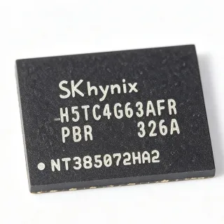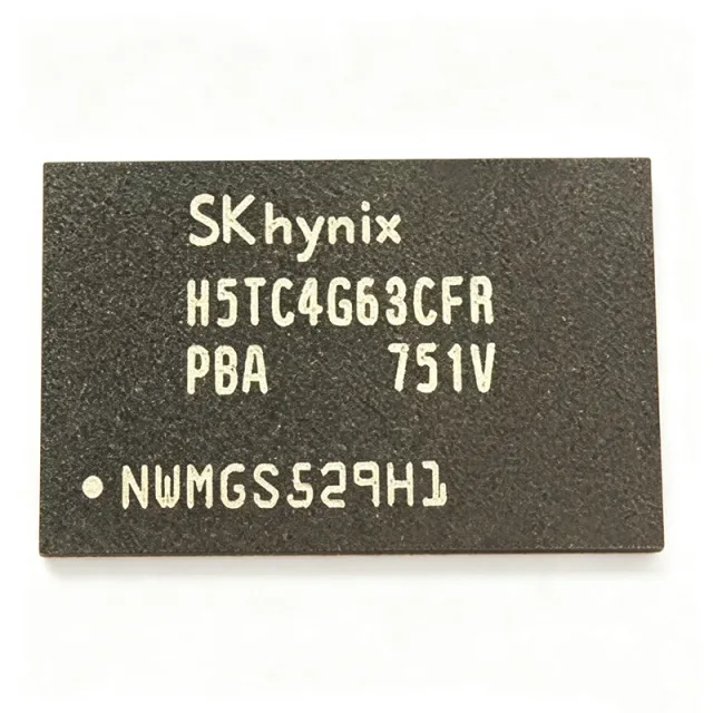
H5TC4G63CFR-PBA - 4Gb DDR3L SDRAM 256Mx16 | SK Hynix
MPN: H5TC4G63CFR-PBA ✓ Active| Qty | Unit Price | Extended |
|---|---|---|
| 1 | $10.39 | $10.39 |
| 10 | $9.35 | $93.50 |
| 100 | $8.31 | $831.00 |
| 500 | $7.27 | $3,635.00 |
| 1,000 | $6.23 | $6,230.00 |
Drop-in alternatives for H5TC4G63CFR-PBA — same package, pin-to-pin compatible. Different-package parts requiring PCB rework are excluded.
Quick Comparison Tool — Select alternative parts for side-by-side comparison:
H5TC4G63MFR-PBA
✓ In Stock
$6.5 / Unit
View Datasheet →H5TC4G63AFR-PBI
✓ In Stock
$6.5 / Unit
View Datasheet →H5TC4G63CFR-xxJ
✓ In Stock
$5.9 / Unit
View Datasheet →MT41K256M16RE-15E:D
✓ In Stock
$7.2 / Unit
View Datasheet →MT41K256M16HA-15EM:E
✓ In Stock
$5.95 / Unit
View Datasheet →K4B4G1646E-BMK0
✓ In Stock
$6.5 / Unit
View Datasheet →H5TC4G63CFR-PBA Maximum Ratings & Electrical Characteristics
| Memory Type | DDR3L SDRAM |
| Density | 4Gb |
| Organization | 256M x 16 |
| Supply Voltage (VDD/VDDQ) | 1.35V +0.100/-0.067V |
| Package | 96-ball FBGA (PBGA96) |
| Clock Input | Fully differential (CK, CK) |
| Data Strobe | Differential (DQS, DQS) |
| On-chip DLL | Yes |
| Data Mask (DM) | Yes |
| Auto Precharge | Yes |
| Auto Self-Refresh | Yes |
| Dynamic ODT | Yes |
| ZQ Calibration | Yes |
| Write Leveling | Yes |
| Asynchronous Reset | Yes |
| RoHS | Compliant |
| Halogen-Free | Yes |
| Lead-Free | Yes |
H5TC4G63CFR-PBA Pin Configuration
| Pin A1 | VDD — Power supply |
| Pin A2 | DQ0 — Data input/output 0 |
| Pin A3 | DQ1 — Data input/output 1 |
| Pin A4 | VSS — Ground |
| Pin A5 | DQ2 — Data input/output 2 |
| Pin A6 | DQ3 — Data input/output 3 |
| Pin A7 | VDDQ — Output power supply |
| Pin A8 | DQ4 — Data input/output 4 |
| Pin A9 | DQ5 — Data input/output 5 |
| Pin A10 | VSS — Ground |
| Pin A11 | DQ6 — Data input/output 6 |
| Pin A12 | DQ7 — Data input/output 7 |
| Pin B1 | VSS — Ground |
| Pin B2 | DQS — Data strobe |
| Pin B3 | DQS# — Data strobe complement |
| Pin B4 | VDDQ — Output power supply |
| Pin B5 | DM — Data mask |
| Pin B6 | VSS — Ground |
| Pin B7 | CK — Clock input |
| Pin B8 | CK# — Clock input complement |
| Pin B9 | VDD — Power supply |
| Pin B10 | CKE — Clock enable |
| Pin B11 | CS# — Chip select |
| Pin B12 | RAS# — Row address strobe |
Safe Operating Area (SOA) & Thermal Characteristics
No official SOA curve available for this digital IC. Always operate within absolute maximum ratings specified in the datasheet. Ensure adequate cooling and derate as needed.
Typical Applications
H5TC4G63CFR-PBA is suitable for 6 applications: Laptop Memory, Embedded Systems, Networking Equipment, Industrial PCs, Consumer Electronics, Networking Switches.
Laptop Memory
The H5TC4G63CFR-PBA is ideal for laptop memory modules due to its low 1.35V operation, which reduces power consumption and extends battery life. Its 4Gb density and 256M x 16 organization provide sufficient capacity for mainstream laptops. The FBGA-96 package allows compact module designs, and the on-chip DLL ensures reliable high-speed data transfer. When used in SODIMM modules, it supports dual-channel configurations for improved performance. The low voltage also reduces heat generation, enhancing thermal management in thin laptops.
Recommended
Embedded Systems
In embedded systems, the H5TC4G63CFR-PBA provides high-density memory with low power consumption, making it suitable for industrial controllers, IoT gateways, and single-board computers. Its 1.35V operation reduces power supply complexity and heat dissipation. The device supports features like auto self-refresh and dynamic ODT, which simplify system design and improve signal integrity. The FBGA-96 package is space-efficient, ideal for compact PCBs. With a wide operating temperature range, it can handle demanding industrial environments.
Recommended
Networking Equipment
The H5TC4G63CFR-PBA is well-suited for networking equipment such as routers, switches, and firewalls, where high bandwidth and low power are critical. Its 4Gb density supports large routing tables and buffering. The differential clock and strobe inputs ensure reliable data capture at high speeds, essential for packet processing. The low 1.35V supply reduces power consumption in always-on network devices. The FBGA-96 package allows high-density board layouts, and the on-chip DLL minimizes skew, improving signal integrity in high-speed designs.
Recommended
Industrial PCs
Industrial PCs require reliable, high-density memory that can operate in harsh environments. The H5TC4G63CFR-PBA offers 4Gb capacity and low 1.35V operation, reducing power consumption and heat in sealed enclosures. Its robust design includes features like auto self-refresh and write leveling, ensuring data integrity over long operational lifetimes. The FBGA-96 package is resistant to vibration and shock, making it suitable for factory automation and process control. The wide temperature range supports operation in unheated industrial settings.
Recommended
Consumer Electronics
In consumer electronics like smart TVs, set-top boxes, and gaming consoles, the H5TC4G63CFR-PBA provides high-speed memory for smooth multimedia performance. Its 4Gb density supports HD video streaming and multitasking. The low 1.35V operation reduces power consumption, contributing to energy-efficient designs. The FBGA-96 package enables slim product designs. The on-chip DLL and differential signaling ensure stable operation at high clock speeds, delivering the bandwidth needed for graphics and audio processing.
Recommended
Networking Switches
The H5TC4G63CFR-PBA is ideal for networking switches that require high-bandwidth memory for packet buffering and forwarding. Its 4Gb density provides ample storage for MAC address tables and queue management. The low 1.35V supply reduces power consumption in high-port-count switches. The differential clock and strobe inputs ensure precise data timing, critical for line-rate processing. The FBGA-96 package allows dense placement on switch PCBs, and the on-chip DLL minimizes clock skew, enhancing signal integrity in multi-layer boards.
Recommended
Recommended Products Summary
Engineering reference data for H5TC4G63CFR-PBA — comparison, design guidance, and compliance information.
Selection Guide
Comparison with Alternatives
| Parameter | This Product | H5TC4G63MFR-PBA | H5TC4G63AFR-PBI | MT41K256M16RE-15E | MT41K256M16HA-15EM | K4B4G1646E-BMK0 |
|---|---|---|---|---|---|---|
| Package | FBGA-96 | FBGA-96 | FBGA-96 | D: FBGA-96 | E: FBGA-96 | FBGA-96 |
| Brand | SK Hynix | SK Hynix | SK Hynix | D: Micron | E: Micron | Samsung |
| Density | 4Gb | 4Gb | 4Gb | D: 4Gb | E: 4Gb | 4Gb |
| Organization | 256M x 16 | 256M x 16 | 256M x 16 | D: 256M x 16 | E: 256M x 16 | 256M x 16 |
| Supply Voltage | 1.35V | 1.35V | 1.35V | D: 1.35V | E: 1.35V | 1.35V |
| Speed Grade | [DATA_NEEDED: speed grade] | [DATA_NEEDED] | [DATA_NEEDED] | D: DDR3L-1600 | E: DDR3L-1600 | [DATA_NEEDED] |
| RoHS | Compliant | Compliant | Compliant | D: Compliant | E: Compliant | Compliant |
| Operating Temperature | [DATA_NEEDED: operating temperature] | [DATA_NEEDED] | [DATA_NEEDED] | D: 0°C to 95°C | E: 0°C to 95°C | [DATA_NEEDED] |
Key Differentiators
- Low voltage operation at 1.35V (vs Standard DDR3 at 1.5V)
- High density 4Gb in FBGA-96 (vs Lower density parts like 2Gb)
- RoHS and halogen-free compliance (vs Non-compliant parts)
Design Notes
For high-speed DDR3L designs, maintain controlled impedance of 40-50 ohms for DQ, DQS, and clock traces. Use differential routing for CK/CK# and DQS/DQS# pairs with 100-ohm differential impedance. Keep trace lengths matched within 0.5mm to minimize skew. Place decoupling capacitors (0.1uF and 0.01uF) close to each VDD and VDDQ pin, and a bulk capacitor (10uF) near the memory device.
The H5TC4G63CFR-PBA requires a stable 1.35V supply with low noise. Use a dedicated voltage regulator or a low-noise LDO for the VDD and VDDQ rails. Ensure the power supply can handle peak current spikes during read/write operations. Add ferrite beads in series with the power rails to filter high-frequency noise. Monitor the voltage tolerance of +0.100/-0.067V to avoid data corruption.
To maintain signal integrity, use on-die termination (ODT) settings as recommended in the datasheet. For point-to-point connections, set ODT to 40 ohms; for multi-drop, adjust accordingly. Use write leveling to compensate for clock-to-strobe skew. Ensure the reference voltage (VREF) is clean and stable, typically 0.49 * VDDQ. Follow the layout guidelines for VREF routing to avoid noise coupling.
Compliance Information
RoHS compliant and halogen-free per datasheet. AEC-Q100 not applicable as this is a memory component.