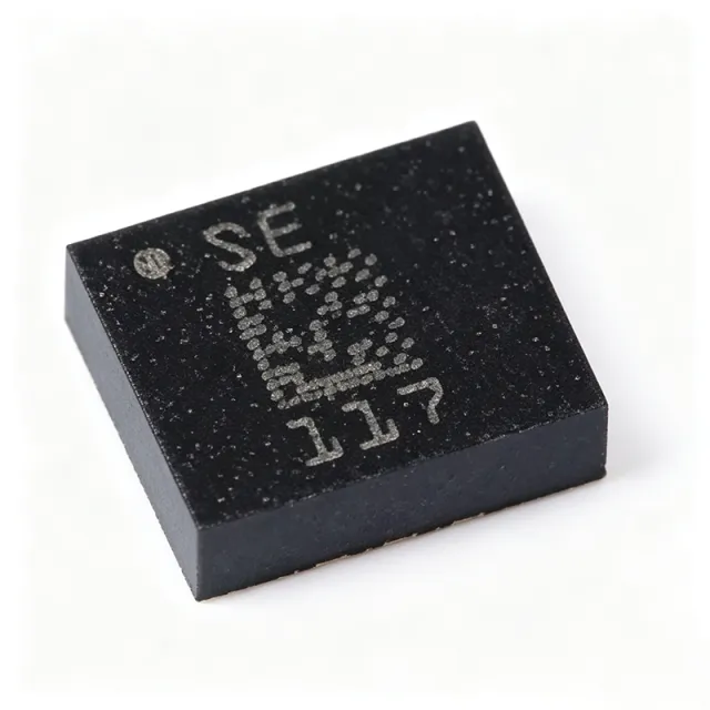
LSM6DS3TR-C - 3D Accelerometer & 3D Gyroscope | STMicroelectronics
MPN: LSM6DS3TR-C ✓ Active| Qty | Unit Price | Extended |
|---|---|---|
| 1 | $1.5 | $1.50 |
| 10 | $1.0833 | $10.83 |
| 100 | $0.9583 | $95.83 |
| 500 | $0.9167 | $458.35 |
| 1,000 | $0.875 | $875.00 |
Drop-in alternatives for LSM6DS3TR-C — same package, pin-to-pin compatible. Different-package parts requiring PCB rework are excluded.
Quick Comparison Tool — Select alternative parts for side-by-side comparison:
LSM6DS3
📋 Reference alternative (not in catalog)
LSM6DSO
📋 Reference alternative (not in catalog)
LSM6DSLTR
✓ In Stock
$1.85 / Unit
View Datasheet →LSM6DS3TR-C Maximum Ratings & Electrical Characteristics
| Accelerometer Full-Scale Range | ±2/±4/±8/±16 g |
| Gyroscope Full-Scale Range | ±125/±245/±500/±1000/±2000 dps |
| Output Data Rate (ODR) | 1.6 Hz to 6.66 kHz (accel), 12.5 Hz to 6.66 kHz (gyro) |
| Resolution | 16-bit |
| Supply Voltage | 1.71 V to 3.6 V |
| Current Consumption (Normal Mode) | 0.9 mA |
| Current Consumption (Low Power Mode) | 0.45 mA |
| FIFO Size | 8 KB |
| Communication Interface | I2C, SPI |
| Package | LGA-14L (2.5 x 3.0 x 0.83 mm) |
| Operating Temperature Range | -40°C to +85°C |
| Sensitivity (Accel) | 0.061 mg/LSB (at ±2g) |
| Sensitivity (Gyro) | 4.375 mdps/LSB (at ±125dps) |
| Zero-g Offset (Accel) | ±20 mg |
| Zero-rate Offset (Gyro) | ±10 dps |
| RoHS Status | Compliant |
LSM6DS3TR-C Pin Configuration
| Pin 1 | VDD_IO — Power supply for I/O pins |
| Pin 2 | SCL/SPC — I2C clock / SPI clock |
| Pin 3 | SDA/SDI — I2C data / SPI data input |
| Pin 4 | SDO/SA0 — SPI data output / I2C address select |
| Pin 5 | CS — Chip select (active low) |
| Pin 6 | INT1 — Interrupt 1 output |
| Pin 7 | INT2 — Interrupt 2 output |
| Pin 8 | GND — Ground |
| Pin 9 | GND — Ground |
| Pin 10 | VDD — Power supply |
| Pin 11 | NC — Not connected |
| Pin 12 | NC — Not connected |
| Pin 13 | NC — Not connected |
| Pin 14 | NC — Not connected |
Safe Operating Area (SOA) & Thermal Characteristics
No official SOA curve available for this component. Always operate within absolute maximum ratings specified in the datasheet. Ensure adequate cooling and derate as needed.
Typical Applications
LSM6DS3TR-C is suitable for 6 applications: Wearable Fitness Trackers, Smartphones and Tablets, Industrial Vibration Monitoring, Gaming and Virtual Reality, IoT Smart Home Devices, Optical Image Stabilization (OIS).
Wearable Fitness Trackers
The LSM6DS3TR-C is ideal for wearable fitness trackers due to its ultra-low power consumption (0.9 mA) and compact LGA-14L package. It enables continuous step counting, activity recognition, and sleep monitoring without draining the battery. The hardware step detector and pedometer offload the host MCU, allowing the main processor to remain in sleep mode longer. The 16-bit resolution and wide full-scale ranges (±2g to ±16g) ensure accurate motion tracking across various activities, from walking to vigorous exercise. The device's small footprint (2.5x3.0x0.83 mm) fits easily into slim wearable designs, and its I2C/SPI interface simplifies integration with common MCUs like nRF52 or STM32. Designers should ensure proper power supply decoupling and place the sensor away from high-frequency traces to minimize noise. The FIFO buffer can store motion data during high-activity periods, reducing host wake-ups and further saving power.
Recommended
Smartphones and Tablets
In smartphones and tablets, the LSM6DS3TR-C provides motion sensing for screen rotation, gesture recognition, and gaming. Its low power consumption is critical for always-on functions like step counting and tilt detection. The device's high sensitivity (0.061 mg/LSB at ±2g) ensures precise orientation detection, while the gyroscope's range up to ±2000 dps supports fast motion in gaming. The embedded FIFO and interrupt engine allow the application processor to stay in low-power states, waking only when motion events occur. The I2C interface at up to 400 kHz or SPI at up to 10 MHz provides fast data transfer. Designers should place the sensor near the device's center of mass for accurate motion sensing and avoid mounting near speakers or vibration sources. The device's small size and low profile make it suitable for slim smartphone designs.
Recommended
Industrial Vibration Monitoring
The LSM6DS3TR-C is suitable for industrial vibration monitoring due to its wide full-scale range (±16g) and high resolution (16-bit). It can detect vibrations in machinery, enabling predictive maintenance. The device's operating temperature range of -40°C to +85°C allows deployment in harsh industrial environments. The SPI interface enables high-speed data streaming for real-time analysis. The embedded FIFO can buffer vibration data for post-processing, reducing host load. Designers should mount the sensor securely to the monitored equipment to ensure accurate vibration transfer. The device's low power consumption is beneficial for battery-powered wireless sensor nodes. The interrupt engine can be configured to trigger alerts when vibration thresholds are exceeded, enabling immediate response to anomalies.
Recommended
Gaming and Virtual Reality
The LSM6DS3TR-C provides high-speed motion tracking for gaming controllers and VR headsets. Its gyroscope range up to ±2000 dps captures rapid movements, while the accelerometer's ±16g range handles sudden impacts. The device's low latency and high ODR (up to 6.66 kHz) ensure responsive tracking. The 16-bit resolution provides smooth, accurate motion data. The I2C/SPI interface allows integration with gaming MCUs. Designers should minimize latency by using the SPI interface and configuring the device for high ODR. The FIFO can be used to batch data, reducing interrupt overhead. The device's small size is ideal for compact controllers. Power consumption is less critical in gaming devices, but the low-power modes are still useful for wireless controllers.
Recommended
IoT Smart Home Devices
The LSM6DS3TR-C is perfect for IoT smart home devices like smart thermostats, security cameras, and smart speakers. Its low power consumption enables battery-powered operation for years. The device can detect motion for security alerts or presence detection. The always-on feature with interrupt generation allows the system to wake only when motion is detected, saving power. The compact package fits into small devices. The I2C interface simplifies connection to low-power MCUs like ESP32 or STM32L0. Designers should place the sensor to detect relevant motion and configure the interrupt thresholds appropriately. The FIFO can store motion events for later retrieval. The device's wide temperature range ensures reliable operation in various home environments.
Recommended
Optical Image Stabilization (OIS)
The LSM6DS3TR-C is used in camera modules for optical image stabilization, where the gyroscope detects camera shake and the system compensates by moving the lens or sensor. The gyroscope's high sensitivity (4.375 mdps/LSB at ±125dps) and low noise are critical for accurate stabilization. The device's high ODR (up to 6.66 kHz) ensures real-time correction. The small package allows integration into compact camera modules. The SPI interface provides high-speed data transfer to the OIS controller. Designers should mount the sensor close to the camera module and ensure mechanical coupling to detect shake accurately. The device's low power consumption is beneficial for battery-powered cameras. The FIFO can buffer gyro data for processing.
Recommended
Recommended Products Summary
Engineering reference data for LSM6DS3TR-C — comparison, design guidance, and compliance information.
Selection Guide
Comparison with Alternatives
| Parameter | This Product | LSM6DS3 | LSM6DSO | LSM6DSL |
|---|---|---|---|---|
| Package | LGA-14L | LGA-14L - same | LGA-14L - same | LGA-14L - same |
| Accelerometer Full-Scale Range | ±2/±4/±8/±16 g | ±2/±4/±8/±16 g | ±2/±4/±8/±16 g | ±2/±4/±8/±16 g |
| Gyroscope Full-Scale Range | ±125/±245/±500/±1000/±2000 dps | ±125/±245/±500/±1000/±2000 dps | ±125/±245/±500/±1000/±2000 dps | ±125/±245/±500/±1000/±2000 dps |
| Current Consumption (Normal Mode) | 0.9 mA | 0.9 mA | 0.55 mA | 0.45 mA |
| FIFO Size | 8 KB | 8 KB | 3 KB | 4 KB |
| Output Data Rate (Max) | 6.66 kHz | 6.66 kHz | 6.66 kHz | 6.66 kHz |
| Supply Voltage Range | 1.71V to 3.6V | 1.71V to 3.6V | 1.71V to 3.6V | 1.71V to 3.6V |
| Operating Temperature Range | -40°C to +85°C | -40°C to +85°C | -40°C to +85°C | -40°C to +85°C |
Key Differentiators
- Larger FIFO (8 KB) compared to LSM6DSO (3 KB) (vs LSM6DSO)
- Lower current consumption (0.9 mA) than LSM6DSO (0.55 mA) (vs LSM6DSO)
- Pin-to-pin compatible with LSM6DS3 (vs LSM6DS3)
Design Notes
Place a 100 nF decoupling capacitor close to the VDD pin and a 100 nF capacitor on VDD_IO. Use a low-ESR ceramic capacitor to ensure stable operation. The supply voltage should be within 1.71V to 3.6V; avoid voltage drops below the minimum to prevent malfunction.
Route I2C/SPI traces with minimal length and avoid crossing high-speed digital lines. Use ground planes to reduce noise. Place the sensor away from heat sources and mechanical stress points. Ensure proper soldering of the LGA package to avoid cold joints.
Do not exceed the absolute maximum ratings, including supply voltage and acceleration. Ensure the I2C address is correctly set via the SDO/SA0 pin to avoid address conflicts. Configure the ODR and full-scale ranges appropriately for the application to avoid data overflow.
Compliance Information
RoHS compliant per STMicroelectronics datasheet. Not AEC-Q100 qualified.