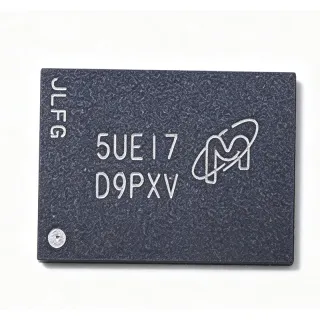
MT41K512M8DA-107 IT:P - 4Gb DDR3L SDRAM x8 | Micron
MPN: MT41K512M8DA-107 IT:P ✓ Active| Qty | Unit Price | Extended |
|---|---|---|
| 1 | $66.4 | $66.40 |
| 10 | $63.08 | $630.80 |
| 100 | $59.76 | $5,976.00 |
| 500 | $56.44 | $28,220.00 |
| 1,000 | $53.12 | $53,120.00 |
MT41K512M8DA-107 IT:P Overview
A DDR3 SDRAM (Double Data Rate Type Three Synchronous Dynamic Random Access Memory) is a type of volatile memory IC that transfers data on both clock edges, doubling bandwidth relative to single data rate DRAM at the same clock frequency. Within the memory hierarchy it sits as main-system memory, alongside DRAM controllers, memory ICs, and semiconductor components in the broader integrated circuit taxonomy. DDR3 operates at 1.5V and uses an 8n prefetch architecture, on-die termination (ODT), write leveling, and auto self-refresh to sustain high data rates while managing signal integrity.
Key features of this part per distributor data include 4Gbit density in a x8 organization, Auto self-refresh, Auto precharge, an asynchronous reset function, data mask capability, dynamic on-die termination, and write leveling. The industrial temperature range (-40C to +95C) makes it suitable for environments beyond standard commercial 0C to +85C operation, and the TFBGA ball-grid package provides short, low-inductance interconnects for high-speed signal routing.
Architecturally, the 512M x 8 organization maps to internal banks accessed through a standard DDR3 command interface with RAS, CAS, WE, chip select, bank address, and row/column address pins. The -107 grade supports DDR3-1866 timing, requiring a memory controller configured for the corresponding JEDEC speed bin. Designers must confirm exact CAS latency, tRCD, tRP, and supply class (1.5V vs 1.35V DDR3L) from the official Micron datasheet before finalizing a design.
Typical applications include industrial control and automation systems, networking and communication equipment, test and measurement instrumentation, and embedded computing platforms that require high-density DRAM with industrial-grade temperature tolerance.
A key design consideration: DDR3 signal integrity at 1866 Mbps requires careful fly-by termination routing, matched trace lengths, and ODT calibration; the 78-ball TFBGA footprint also demands precise PCB land pattern adherence per the Micron package drawing.
This page synthesizes distributor inventory data, the verified industrial-temperature and RoHS suffix coding, and family cross-reference information not consolidated in the manufacturer datasheet.
Drop-in alternatives for MT41K512M8DA-107 IT:P — same package, pin-to-pin compatible. Different-package parts requiring PCB rework are excluded.
Quick Comparison Tool — Select alternative parts for side-by-side comparison:
MT41K512M8DA-107:P
✅ Drop-In ⚠️ 参数待验证📋 Reference alternative (not in catalog)
MT41K512M8DA-125 IT:P
✅ Drop-In ⚠️ 参数待验证📋 Reference alternative (not in catalog)
MT41K512M8DA-093 IT:P
✅ Drop-In ⚠️ 参数待验证📋 Reference alternative (not in catalog)
MT41K512M8DA-107 IT:P Maximum Ratings & Electrical Characteristics
| Memory Type | DDR3 SDRAM |
| Memory Size | 4 Gbit |
| Organization | 512M x 8 |
| Speed Grade | -107 (DDR3-1866 class) |
| Interface | Parallel DDR3 |
| Package | TFBGA-78 |
| Operating Temperature | -40C to +95C (Industrial, IT suffix) |
| Refresh | Auto self-refresh (per LCSC listing) |
| Auto Precharge | Supported (per LCSC listing) |
| Asynchronous Reset | Supported (per LCSC listing) |
| Data Mask | Supported (per LCSC listing) |
| On-Die Termination | Dynamic ODT (per LCSC listing) |
| Write Leveling | Supported (per LCSC listing) |
| Mounting Type | Surface Mount |
| RoHS Status | Compliant (P suffix, lead-free) |
MT41K512M8DA-107 IT:P tfbga-78 Pin Configuration Guide
Pin configuration for MT41K512M8DA-107 IT:P (tfbga-78 package). This digital IC includes GPIO, communication interfaces (UART, SPI, I2C), and power pins. Refer to the manufacturer datasheet for alternate pin functions and configuration options. Essential for embedded system design and PCB layout.

No detailed pinout data available for MT41K512M8DA-107 IT:P.
Refer to the datasheet for full pin configuration.
Typical Applications
MT41K512M8DA-107 IT:P is suitable for 6 applications: Industrial Control and Automation, Networking and Communication Equipment, Test and Measurement Instrumentation, Embedded Computing and Industrial PCs, Transportation and Telematics Electronics, Security and Video Surveillance Systems.
Industrial Control and Automation
The MT41K512M8DA-107 IT:P fits industrial controllers, PLCs, and robot control boards because its IT suffix guarantees -40C to +95C operation across factory-floor ambient extremes that exceed commercial DRAM ratings. Its 4Gb (512M x 8) density supports real-time operating systems, motion-control firmware, and data logging buffers without external memory expansion. The asynchronous reset function allows the host to recover the DRAM cleanly after industrial power disturbances, while auto self-refresh preserves contents during low-power or hold states. Dynamic on-die termination and write leveling simplify meeting DDR3-1866-class signal integrity on long, backplane-adjacent traces typical of control cabinets. Designers should route the 78-ball TFBGA with fly-by termination and verify controller ODT calibration against the official Micron datasheet speed-bin table.
Recommended
Networking and Communication Equipment
Enterprise switches, routers, and telecom line cards use DDR3 SDRAM as packet-buffer and control-plane memory, and the MT41K512M8DA-107 IT:P suits both indoor rack environments and temperature-hardened outdoor plant. The -107 speed grade provides DDR3-1866-class bandwidth to sustain line-rate packet processing, while the 512M x 8 organization maps efficiently to common memory-controller data widths, with byte-lane data mask supporting partial writes of packet headers. The TFBGA-78 package keeps interconnect inductance low for high-speed DQS/DQ signaling at 1866 Mbps. Dynamic ODT compensates for varying topologies when multiple ranks are populated, and auto precharge reduces controller overhead in random-access buffer patterns. Verify the exact CAS latency bin from the Micron datasheet before configuring the controller.
Recommended
Test and Measurement Instrumentation
Oscilloscopes, logic analyzers, and spectrum analyzers require deep capture memory with high sustained bandwidth, and the MT41K512M8DA-107 IT:P provides 4Gb of DDR3-1866-class storage in a compact 78-ball TFBGA. Bench instruments benefit from the industrial -40C to +95C rating when deployed in unconditioned field or vehicle-mounted measurement systems. The data mask function enables efficient waveform-buffer updates without full-burst write penalties, and write leveling ensures reliable DQS alignment across the trace-length skew typical of wide capture buses. Auto self-refresh preserves data through instrument standby states. Engineers should budget controller timing for the -107 speed bin and follow Micron's termination guidance to maintain eye margin at full data rate across the operating temperature range.
Recommended
Embedded Computing and Industrial PCs
Fanless embedded PCs, edge gateways, and single-board computers use the MT41K512M8DA-107 IT:P as main memory where the IT:P industrial qualification matches enclosure temperatures that can exceed commercial limits in sealed, passively cooled housings. The 4Gb density supports Linux or RTOS stacks plus application caching, and the x8 organization allows two or four devices to be ganged for 64-bit controllers with independent rank control. DDR3's asynchronous reset and auto self-refresh support S3-style suspend paths in battery-backed gateways. The TFBGA-78 footprint fits dense SO-DIMM-style or soldered-down memory designs. Layout engineers should apply fly-by clock routing, matched DQ/DQS skew windows, and per the Micron datasheet, program controller ODT and drive-strength settings to the -107 speed bin.
Recommended
Transportation and Telematics Electronics
Trackside communications, fleet telematics, and railway signaling equipment experience wide ambient swings, making the -40C to +95C industrial rating of the MT41K512M8DA-107 IT:P a direct fit where commercial-grade DRAM would be derated or unreliable. The 4Gb capacity stores map data, event logs, and protocol stacks for gateways and onboard units. Auto self-refresh maintains memory contents through engine-off or low-power hold modes, and the asynchronous reset pin supports watchdog-triggered recovery after supply transients. The 78-ball TFBGA package withstands vibration better than fine-pitch leaded packages due to its compliant ball interconnect. Designers must still verify solder-joint reliability expectations and reflow profiles against the Micron package specification for their shock/vibration class.
Recommended
Security and Video Surveillance Systems
Network video recorders, AI-enabled IP cameras, and video management appliances buffer multiple high-resolution streams, and the MT41K512M8DA-107 IT:P supplies 4Gb of DDR3-1866-class working memory for frame buffers, analytics pipelines, and database caching. Outdoor and pole-mounted enclosures routinely reach temperature extremes covered by the -40C to +95C industrial rating. The data mask function reduces write traffic when only metadata regions of a frame buffer change, and dynamic on-die termination maintains signal integrity as bus loading varies. The x8 organization lets designers scale to 32-bit or 64-bit buses with uniform byte-lane routing from the 78-ball TFBGA footprint. Confirm the datasheet speed-bin latency values so stream-processing throughput meets the frame-rate budget.
Recommended
Recommended Products Summary
Engineering reference data for MT41K512M8DA-107 IT:P — comparison, design guidance, and compliance information.
Selection Guide
Comparison with Alternatives
| Parameter | This Product | MT41K512M8DA-107:P | MT41K512M8DA-125 IT:P | MT41K512M8DA-093 IT:P | MT41K512M16VRP-107 |
|---|---|---|---|---|---|
| Package | TFBGA-78 | TFBGA-78 - same | TFBGA-78 - same | TFBGA-78 - same | Different TFBGA ballout (x16) |
| Brand | Micron Technology | Micron Technology | Micron Technology | Micron Technology | Micron Technology |
| Memory Size | 4 Gbit | 4 Gbit | 4 Gbit | 4 Gbit | 4 Gbit |
| Organization | 512M x 8 | 512M x 8 | 512M x 8 | 512M x 8 | 256M x 16 |
| Speed Grade | -107 (DDR3-1866 class) | -107 (DDR3-1866 class) | -125 (DDR3-1600 class) | -093 (DDR3-2133 class) | -107 (DDR3-1866 class) |
| Operating Temperature | -40C to +95C (Industrial) | 0C to +85C (Commercial) | -40C to +95C (Industrial) | -40C to +95C (Industrial) | -40C to +95C (Industrial) |
| Self-Refresh / ODT Features | Auto self-refresh, dynamic ODT, write leveling | Same feature set | Same feature set | Same feature set | Same feature set (x16 bus) |
| RoHS / Lead-Free | Yes (P suffix) | Yes (P suffix) | Yes (P suffix) | Yes (P suffix) | Yes (P suffix) |
Key Differentiators
- Industrial temperature qualification (vs MT41K512M8DA-107:P)
- Higher speed margin option in same footprint (vs MT41K512M8DA-125 IT:P)
- Compact x8 organization for scalable buses (vs MT41K512M16VRP-107)
Design Notes
At DDR3-1866-class data rates, route address/command lines in fly-by topology with per-byte-lane DQS/DQ matched-length groups; keep skew within the controller's leveling window. Enable write leveling during controller training to compensate for trace-length mismatch across the 78-ball TFBGA footprint. Dynamic ODT should be programmed per the Micron datasheet speed-bin table rather than copied from another design, since ODT values interact with drive strength and termination topology.
Confirm the supply-voltage class (1.5V DDR3 vs 1.35V DDR3L) from the official Micron datasheet ordering table before designing the power tree - the IT:P suffix encodes temperature and plating, not voltage class. Estimated: a single 4Gb DDR3 device can draw several hundred mA peak at full bandwidth, so decouple VDD and VDDQ with bulk plus high-frequency ceramics close to each ball and verify the regulator's transient response against burst-write load steps.
Follow Micron's exact TFBGA-78 land pattern (non-solder-mask-defined pads) and use the reflow profile from the package specification. Place the DRAM within short trace length of the memory controller, dedicate solid ground planes beneath DQ/DQS routing, and avoid crossing plane splits. For industrial -40C to +95C deployments, account for solder-joint reliability across thermal cycling when choosing ball-attach and assembly parameters.
Compliance Information
P suffix denotes lead-free, RoHS-compliant construction per Micron ordering-code convention and distributor listings. REACH, halogen-free, and conflict-minerals statuses not found in provided data - confirm via Micron compliance documentation.