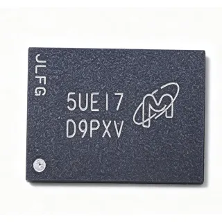
MT62F1536M64D8EK-023 - 96Gbit LPDDR5X SDRAM | Micron | Mobile
MPN: MT62F1536M64D8EK-023 ✓ Active| Qty | Unit Price | Extended |
|---|---|---|
| 1 | $1 | $1.00 |
Drop-in alternatives for MT62F1536M64D8EK-023 — same package, pin-to-pin compatible. Different-package parts requiring PCB rework are excluded.
Quick Comparison Tool — Select alternative parts for side-by-side comparison:
MT62F1536M64D8EK-023 AIT:C
✅ Drop-In📋 Reference alternative (not in catalog)
MT62F1536M64D8EK-023 AAT:C
✅ Drop-In📋 Reference alternative (not in catalog)
MT62F1536M64D8EK-023 AUT:C
✅ Drop-In📋 Reference alternative (not in catalog)
MT62F1536M64D8EK-023 WT:B
✅ Drop-In📋 Reference alternative (not in catalog)
MT62F1536M64D8EK-023 WT:D
✅ Drop-In📋 Reference alternative (not in catalog)
MT62F1536M64D8EK-023 Maximum Ratings & Electrical Characteristics
| Memory Type | Mobile LPDDR5X SDRAM |
| Memory Size | 96 Gbit (12 GB) |
| Organization | 1.5G x 64 |
| Clock Frequency | 4.266 GHz |
| Memory Interface | LVSTL |
| Supply Voltage | 1.01 V to 1.12 V |
| Package | 441-TFBGA (14 x 14 mm) |
| Mounting Type | Surface Mount |
| Ball Count | 441 |
| Package Body Size | 14 mm x 14 mm |
| Data Bus Width | 64-bit |
| Speed Grade | -023 (4266 class) |
MT62F1536M64D8EK-023 14 mm x 14 mm Pin Configuration Guide
Complete pinout information for MT62F1536M64D8EK-023 (14 mm x 14 mm package). This digital IC includes GPIO, communication interfaces (UART, SPI, I2C), and power pins. Refer to the manufacturer datasheet for alternate pin functions and configuration options. Essential for embedded system design and PCB layout.

No detailed pinout data available for MT62F1536M64D8EK-023.
Refer to the datasheet for full pin configuration.
Safe Operating Area (SOA) & Thermal Characteristics
No official SOA curve available for this digital IC. Always operate within absolute maximum ratings specified in the datasheet. Ensure adequate cooling and derate as needed.
Typical Applications
MT62F1536M64D8EK-023 is suitable for 6 applications: Flagship Smartphone Main Memory, Automotive Infotainment and ADAS, Tablet and Notebook LPDDR5X Memory, Edge AI and Robotics Modules, 5G Networking and Edge Servers, AR/VR and Wearable Compute.
Flagship Smartphone Main Memory
The MT62F1536M64D8EK-023 delivers 12 GB of LPDDR5X main memory in a single 441-TFBGA (14 x 14 mm) package, which is the standard main-memory configuration for flagship smartphones. Its 4.266 GHz LPDDR5X data rate with LVSTL signaling provides the bandwidth that flagship mobile SoCs require for multitasking, high-refresh-rate displays, and computational photography pipelines, while the 1.01 V to 1.12 V core voltage keeps dynamic power within smartphone battery budgets. In a typical design, the device sits directly adjacent to the application processor on the same PCB or inside a stacked PoP assembly, with the CA and DQ buses length-matched to the SoC's memory-controller fly-by topology. Because LPDDR5X supports per-bank refresh and DVFS, the PMIC can scale VDDQ down during idle states, measurably extending standby battery life compared with fixed-voltage LPDDR4 designs.
Recommended
Automotive Infotainment and ADAS
For automotive cockpit and ADAS platforms, the AEC-Q100 qualified grade variants (AIT and AUT suffixes) of this 96 Gbit LPDDR5X device bring 4.266 GHz bandwidth to next-generation domain controllers. Automotive infotainment SoCs driving multiple high-resolution displays and surround-view camera fusion require the multi-gigabyte-per-second memory bandwidth that LPDDR5X provides, while the -40C to +95C AIT operating range covers the harsh cabin and engine-bay-adjacent environments defined by automotive qualification. The same 441-TFBGA (14 x 14 mm) footprint as the commercial WT grade means a single PCB design can serve both consumer and automotive product lines, simplifying platform reuse. Designers should confirm the SoC's LPDDR5X speed-bin support and apply the automotive-grade PMIC companion parts that implement the fault monitoring and voltage-margining expected in ASIL-relevant memory subsystems.
Recommended
Tablet and Notebook LPDDR5X Memory
Mainstream tablets and thin-and-light notebooks adopt LPDDR5X to reach desktop-class memory bandwidth while meeting fanless thermal envelopes. The MT62F1536M64D8EK-023 provides a complete 64-bit, 12 GB memory channel in one 14 x 14 mm package, and two packages can be paired for 24 GB in wide 128-bit configurations where the SoC supports dual channels. Its 1.01 V to 1.12 V supply window allows the platform PMIC to exploit LPDDR5X dynamic voltage scaling, reducing platform power during light workloads - a key contributor to all-day battery life targets. On the PCB, the memory should be placed within the SoC's specified trace-length window, and the LVSTL I/O structure requires the controller-side termination scheme defined in the LPDDR5X specification. Thermal design should account for DRAM refresh current under sustained AI or media workloads.
Recommended
Edge AI and Robotics Modules
Edge AI accelerator modules and autonomous robotics controllers need large on-board DRAM for neural network weight storage, frame buffers, and sensor fusion pipelines, but cannot afford the power of DDR5 server memory. The MT62F1536M64D8EK-023's combination of 12 GB capacity and 4.266 GHz LPDDR5X throughput supplies the memory bandwidth that inference accelerators demand for real-time vision models, while the low 1.01 V to 1.12 V rail keeps module power within passive-cooled budgets. The 441-TFBGA (14 x 14 mm) package integrates cleanly into SOM (system-on-module) form factors such as the 60 x 45 mm embedded standard. The extended-temperature AAT variant, rated -40C to +105C, suits industrial robots and outdoor edge enclosures. Verify the accelerator SoC's memory-controller calibration supports the -023 speed bin at full temperature range.
Recommended
5G Networking and Edge Servers
5G small-cell baseband units, network appliances, and micro-edge servers increasingly use LPDDR5X instead of DDR4 DIMMs to save board space and power in fanless enclosures. The MT62F1536M64D8EK-023 offers 12 GB per package with a 64-bit bus at 4.266 GHz, enough for packet buffering, DPI rule sets, and virtualized network functions at the network edge. Compared with a discrete DDR4 solution, the LPDDR5X device eliminates the DIMM connector, reduces the memory power rail from 1.2 V to the 1.01 V to 1.12 V window, and cuts PCB area with the 14 x 14 mm TFBGA. Networking SoCs with integrated LPDDR5X controllers can pair one or two of these devices with commodity NOR flash for boot. Use the WT commercial grade for indoor telecom equipment and the AIT grade for outdoor-mounted radios.
Recommended
AR/VR and Wearable Compute
Augmented-reality headsets and advanced wearable compute platforms are among the most power-constrained high-bandwidth systems in existence: they must sustain multi-gigabyte-per-second memory traffic for display pipelines, SLAM tracking, and on-device AI within a battery and thermal budget measured in a few watts. The MT62F1536M64D8EK-023 addresses this directly, providing 12 GB at LPDDR5X 4.266 GHz speeds with LVSTL low-swing I/O that minimizes per-transfer energy, all in a compact 441-ball, 14 x 14 mm TFBGA that fits the tight board geometry of headset mainboards. The 1.01 V to 1.12 V DVFS-capable rail lets the system drop memory voltage aggressively during idle gaze periods, measurably extending session battery life. Design teams should co-locate the DRAM with the XR SoC and follow the controller's fly-by routing constraints to preserve signal integrity at full data rate.
Recommended
Recommended Products Summary
Engineering reference data for MT62F1536M64D8EK-023 — comparison, design guidance, and compliance information.
Selection Guide
Comparison with Alternatives
| Parameter | This Product | MT62F1536M64D8EK-023 AIT:C | MT62F1536M64D8EK-023 AAT:C | MT62F1536M64D8EK-023 WT:B | MT62F1536M64D8EK-023 WT:D |
|---|---|---|---|---|---|
| Package | 441-TFBGA (14 x 14 mm) | 441-TFBGA (14 x 14 mm) - same | 441-TFBGA (14 x 14 mm) - same | 441-TFBGA (14 x 14 mm) - same | 441-TFBGA (14 x 14 mm) - same |
| Brand | Micron Technology | Micron Technology | Micron Technology | Micron Technology | Micron Technology |
| Memory Size | 96 Gbit (12 GB) | 96 Gbit (12 GB) | 96 Gbit (12 GB) | 96 Gbit (12 GB) | 96 Gbit (12 GB) |
| Organization | 1.5G x 64 | 1.5G x 64 | 1.5G x 64 | 1.5G x 64 | 1.5G x 64 |
| Clock Frequency | 4.266 GHz | 4.266 GHz | 4.266 GHz | 4.266 GHz | 4.266 GHz |
| Supply Voltage | 1.01 V to 1.12 V | 1.01 V to 1.12 V | 1.01 V to 1.12 V | 1.01 V to 1.12 V | 1.01 V to 1.12 V |
| Operating Temperature | [DATA_NEEDED] | -40C to +95C | -40C to +105C (TC) | [DATA_NEEDED] | [DATA_NEEDED] |
| Automotive Qualification | No (commercial WT grade) | Yes (AEC-Q100) | Extended temp, non-AEC-Q100 | No (commercial) | No (commercial) |
Key Differentiators
- Automotive-qualified drop-in variant available (vs MT62F1536M64D8EK-023 WT:C (this part))
- Extended temperature coverage (vs MT62F1536M64D8EK-023 AAT:C)
- Highest-tier LPDDR5X speed bin in family (vs MT62F1536M32D4DS-023)
Design Notes
LPDDR5X requires a PMIC with dedicated VDDQ/VDD2 rails supporting dynamic voltage scaling within the 1.01 V to 1.12 V window. Do not power this device from a fixed 1.1 V LDO without DVFS support - the LPDDR5X protocol assumes voltage-margining during training and low-power states. Sequence VDD before or with VDDQ per the Micron power-up specification, and place bulk and 100 nF decoupling capacitors at the ball-side vias to handle multi-ampere transient currents during burst accesses.
Route the CA and DQ buses as length-matched fly-by/point-to-point groups per the SoC memory-controller layout guide. LVSTL signaling at 4.266 GHz demands controlled impedance (typically 40-50 ohm single-ended per controller spec), reference-plane continuity on the layer transitions, and avoiding stubs on DQS strobes. Keep the DRAM within the SoC's maximum trace-length window (typically under 100 mm) and follow the controller's calibration requirements - LPDDR5X read/write training will fail margin checks on out-of-window routing.
Confirm the grade suffix before layout freeze: WT is commercial grade, AIT is AEC-Q100 automotive (-40C to +95C), and AAT extends to -40C to +105C. Mixing grades across a production batch can cause field failures in automotive or industrial environments. Also verify that your SoC's memory controller firmware supports the -023 speed bin and the C-stepping of this device; B and D steppings may require controller init table updates.
Compliance Information
RoHS/REACH status not stated in provided data for the WT grade. The AIT/AUT variants are AEC-Q100 qualified per Newark/Micron listings; the standard WT grade is not an automotive-qualified part.