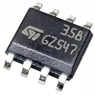
OPA2375IPWR - 10MHz 4.6nV/√Hz Dual CMOS Op Amp | TI
MPN: OPA2375IPWR ✓ Active| Qty | Unit Price | Extended |
|---|---|---|
| 1 | $1.18 | $1.18 |
| 10 | $1.02 | $10.20 |
| 100 | $0.84 | $84.00 |
| 500 | $0.71 | $355.00 |
| 1,000 | $0.62 | $620.00 |
OPA2375IPWR Overview
An operational amplifier (op amp) is a high-gain differential-input voltage amplifier that forms the fundamental building block of analog signal conditioning. Within the voltage regulator-to-amplifier-to-precision-analog hierarchy, the op amp sits between sensors and data converters, conditioning weak signals before digitization. The OPA2375 belongs to the OPAx375 precision CMOS op amp family, which includes the single-channel OPA375 and quad-channel OPA4375 siblings, all sharing the same core amplifier design and RRO output stage.
Key differentiating features include the combination of low noise and wide bandwidth rarely found in general-purpose CMOS op amps, a 500 μV maximum offset voltage enabling precision DC-accurate designs, and rail-to-rail output swing that maximizes dynamic range in low-voltage 5 V and 3.3 V systems. The low-cost CMOS process yields very low input bias currents, suitable for high-impedance sensor front ends.
Architecturally, the OPAx375 family uses a CMOS input stage with a precision-trimmed offset and an output stage that swings to within millivolts of the rails under light load. The 10 MHz bandwidth supports closed-loop gain configurations above 10 V/V while preserving adequate loop gain for low-distortion operation at audio and intermediate frequencies. Supply operation up to 5.5 V suits single-supply portable and industrial logic-level systems.
Typical applications include transducer and photodiode sensor amplifiers, active filter networks, precision current sensing, and buffered analog outputs in industrial automation, medical instrumentation, and battery-powered portable devices. The dual-channel integration saves board area in multi-stage filter and TIA designs.
Design consideration: keep source impedance low to exploit the 4.6 nV/√Hz noise figure, use 0.1 μF decoupling per supply pin, and add an isolation resistor if driving capacitive loads above a few hundred pF in unity gain.
This page synthesizes distributor availability data, same-family drop-in alternatives, and practical design notes not found in the manufacturer datasheet. Pricing shown as of 2026-09-03.
Drop-in alternatives for OPA2375IPWR — same package, pin-to-pin compatible. Different-package parts requiring PCB rework are excluded.
Variants in this series
Same-series models that are drop-in compatible with OPA2375IPWR (same form factor and footprint) — differing in Package, Family, RoHS Status, Input Offset Voltage (Max), Input Voltage Noise.
Quick Comparison Tool — Select alternative parts for side-by-side comparison:
OPA2377IPW
✅ Drop-In ⚠️ Specs Unverified📋 Reference alternative (not in catalog)
OPA2376IPW
✅ Drop-In ⚠️ Specs Unverified📋 Reference alternative (not in catalog)
OPA2320IPW
✅ Drop-In ⚠️ Specs Unverified📋 Reference alternative (not in catalog)
OPA2350IPW
✅ Drop-In ⚠️ Specs Unverified📋 Reference alternative (not in catalog)
TLV2372IPW
✅ Drop-In ⚠️ Specs Unverified📋 Reference alternative (not in catalog)
OPA2375IPWR Maximum Ratings & Electrical Characteristics
| Channels | 2 (Dual) |
| Gain-Bandwidth Product | 10 MHz |
| Input Voltage Noise | 4.6 nV/√Hz (broadband) |
| Input Offset Voltage (Max) | 500 μV |
| Supply Voltage (Max) | 5.5 V |
| Output Type | Rail-to-Rail Output (RRO) |
| Amplifier Technology | CMOS |
| Operating Temperature Range | -40C to +125C (I grade) |
| Package | 8-TSSOP (PW) |
| Mounting Type | Surface Mount |
| Family | OPAx375 (OPA375 / OPA2375 / OPA4375) |
| Typical Applications | Sensors, active filters, TIA, precision analog |
| Lifecycle Status | Active |
| RoHS Status | unknown |
OPA2375IPWR Pin Configuration
| Pin 1 | OUT A — Output of amplifier A |
| Pin 2 | IN A- — Inverting input of amplifier A |
| Pin 3 | IN A+ — Non-inverting input of amplifier A |
| Pin 4 | V- — Negative supply (or GND in single-supply use) |
| Pin 5 | IN B+ — Non-inverting input of amplifier B |
| Pin 6 | IN B- — Inverting input of amplifier B |
| Pin 7 | OUT B — Output of amplifier B |
| Pin 8 | V+ — Positive supply |
Typical Applications
OPA2375IPWR is suitable for 6 applications: Photodiode Transimpedance Amplifier, Active Filter Networks, Precision Current Sensing, Sensor Signal Conditioning in Industrial Automation, Medical and Portable Instrumentation Front Ends, Buffered Analog Outputs and ADC Drivers.
Photodiode Transimpedance Amplifier
The OPA2375IPWR's 4.6 nV/√Hz input noise and CMOS input stage with very low bias current make it a strong choice for photodiode TIA front ends, where amplifier voltage noise is amplified by the noise gain peaking caused by photodiode capacitance. In a typical circuit, the photodiode is reverse-biased into the inverting input with a feedback resistor (e.g., 100 kΩ to 1 MΩ) and a small feedback capacitor for phase-margin compensation. The 10 MHz gain-bandwidth product supports fast signal recovery, and the rail-to-rail output preserves dynamic range at 3.3 V or 5 V single supply. Designers should verify stability by comparing the feedback pole with the noise-gain zero and add an isolation resistor for capacitive loads.
Recommended
Active Filter Networks
Dual-channel integration in one TSSOP-8 package lets designers build two filter stages (e.g., Sallen-Key or multiple-feedback topologies) in a single footprint, saving board area in anti-aliasing and conditioning chains. The OPA2375IPWR's 10 MHz gain-bandwidth product preserves accurate filter corner frequencies up to hundreds of kilohertz even with moderate Q, because loop gain remains high well above the cutoff. Its 4.6 nV/√Hz noise keeps the filter's output noise floor low when resistor values are kept modest, and the 500 μV maximum offset avoids large DC errors in the passband. Use 0.1 μF supply decoupling and keep feedback resistor values below roughly 100 kΩ to limit Johnson noise contribution.
Recommended
Precision Current Sensing
In high-side or low-side current-sense amplification, the OPA2375IPWR's 500 μV maximum input offset voltage translates directly into measurement accuracy: with a 10 mV full-scale shunt, the worst-case offset contributes 5% error before calibration, and typical units perform substantially better. The rail-to-rail output allows the amplifier output to approach the ADC input range limits at 3.3 V or 5 V, while the 10 MHz bandwidth supports fast overcurrent detection loops. Configure as a difference amplifier with 0.1%-matched resistors, or pair with a dedicated instrumentation amplifier for higher common-mode rejection. The dual channels enable simultaneous coarse and fine gain sensing of the same shunt.
Recommended
Sensor Signal Conditioning in Industrial Automation
Factory sensors - pressure bridges, thermocouples, RTD dividers - produce millivolt-level signals that require low-noise amplification before digitization. The OPA2375IPWR delivers 4.6 nV/√Hz noise, so even with a source impedance of several kilohms the amplifier contribution stays well below typical sensor noise. Its industrial -40C to +125C operating range covers panel and field environments, and single-supply 5 V operation matches PLC analog input conventions. One TSSOP-8 package provides two channels, useful for a gain stage followed by a 2nd-order anti-alias filter ahead of the ADC. For microvolt-precision DC measurements, consider pairing or substituting a zero-drift alternative such as the OPA2192.
Recommended
Medical and Portable Instrumentation Front Ends
Battery-powered medical and handheld instruments benefit from the OPA2375IPWR's combination of low noise (4.6 nV/√Hz), low input bias current from the CMOS input stage, and rail-to-rail output that maximizes dynamic range on a single 3.3 V rail. Typical roles include amplifying electrode or biosensor signals, buffering ADC references, and building active filters that remove out-of-band interference. The 10 MHz bandwidth supports intermediate-frequency gain blocks in ultrasonic and optical front ends. The compact 8-TSSOP package suits space-constrained wearable and handheld PCBs. Designers should evaluate total system noise including resistor thermal noise and verify output swing headroom under load for maximum signal swing near the rails.
Recommended
Buffered Analog Outputs and ADC Drivers
The OPA2375IPWR works as a buffer or low-gain driver between a DAC or divider and an ADC input: its RRO stage swings to within millivolts of the rails at light load, and the 10 MHz bandwidth settles quickly for sampling converters in the hundreds-of-kilosamples-per-second class. In unity gain, keep capacitive load below roughly 100 pF or add a small isolation resistor (10-50 Ω) between the output and the load to preserve phase margin. The dual channels allow one amplifier per differential ADC input pair or one signal buffer plus one reference buffer in the same TSSOP-8 footprint. Maintain 0.1 μF decoupling per supply pin close to the IC for clean high-frequency behavior.
Recommended
Recommended Products Summary
Engineering reference data for OPA2375IPWR — comparison, design guidance, and compliance information.
Selection Guide
Comparison with Alternatives
| Parameter | This Product | OPA2377IPW | OPA2376IPW | OPA2320IPW | TLV2372IPW |
|---|---|---|---|---|---|
| Package | 8-TSSOP (PW) | 8-TSSOP (PW) - same | 8-TSSOP (PW) - same | 8-TSSOP (PW) - same | 8-TSSOP (PW) - same |
| Brand | Texas Instruments | Texas Instruments | Texas Instruments | Texas Instruments | Texas Instruments |
| Gain-Bandwidth Product | 10 MHz | 10 MHz (family successor) | 5.5 MHz | 20 MHz | 3 MHz |
| Output Type | Rail-to-Rail Output (RRO) | RRO | RRO | RRIO | RRIO |
| Channels | 2 (Dual) | 2 (Dual) | 2 (Dual) | 2 (Dual) | 2 (Dual) |
| Pin Compatibility | Reference (standard dual op amp pinout) | Pin-to-pin identical | Pin-to-pin identical | Pin-to-pin identical | Pin-to-pin identical |
Key Differentiators
- Lowest noise in its cost class (vs TLV2372IPW)
- Wider bandwidth than the precision sibling (vs OPA2376IPW)
- Balanced noise-bandwidth-cost triangle (vs OPA2377IPW)
Design Notes
Place a 0.1 μF ceramic decoupling capacitor within 2 mm of each supply pin (V+ on pin 8, V- on pin 4), with a shared bulk 2.2-10 μF capacitor per supply rail nearby. A solid ground plane under the TSSOP-8 reduces ground impedance and pickup. Keep high-impedance input traces (pins 2, 3, 5, 6) short and guarded away from switching nodes to exploit the CMOS input stage's low bias current.
Stability with capacitive loads: in unity-gain configurations, output loads above a few hundred picofarads reduce phase margin and can cause ringing or oscillation. Add a series isolation resistor (10-50 Ω) between the output and the capacitive load, or configure a noise-gain above 2. For TIA use, set the feedback capacitor so the feedback pole sits below the noise-gain zero per the standard TI photodiode stability method in the OPAx375 datasheet application section.
Estimated: to exploit the 4.6 nV/√Hz noise figure, keep total source-plus-feedback resistance low - a 100 kΩ resistor alone contributes about 40 nV/√Hz, dwarfing the amplifier noise. Also avoid relying on rail-to-rail output at heavy loads: the RRO stage needs tens of millivolts of headroom from each rail, so design signal swing with margin to avoid clipping near 0 V and 5 V in single-supply systems.
Compliance Information
Compliance details not present in the provided data; verify RoHS/REACH status on the TI product page before design-in.