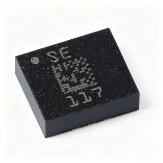
STD5N52K3 - 5A, 525V N-Channel Power MOSFET | STMicroelectronics
MPN: STD5N52K3 ✓ Active| Qty | Unit Price | Extended |
|---|---|---|
| 1 | $0.85 | $0.85 |
| 10 | $0.76 | $7.60 |
| 100 | $0.68 | $68.00 |
| 500 | $0.61 | $305.00 |
| 1,000 | $0.55 | $550.00 |
Drop-in alternatives for STD5N52K3 — same package, pin-to-pin compatible. Different-package parts requiring PCB rework are excluded.
Quick Comparison Tool — Select alternative parts for side-by-side comparison:
STD5N52K3-1
✅ Drop-In📋 Reference alternative (not in catalog)
IPD50N03S4L-08
✅ Drop-In📋 Reference alternative (not in catalog)
NTD5N52
✅ Drop-In📋 Reference alternative (not in catalog)
STD5N52K3 Maximum Ratings & Electrical Characteristics
| Drain-Source Voltage (VDS) | 525 V |
| Continuous Drain Current (ID) at 25°C | 5 A |
| On-Resistance (RDS(on)) | 1.4 Ω typical |
| Gate Charge (Qg) | 15 nC typical |
| Threshold Voltage (VGS(th)) | 3 V to 5 V |
| Package | DPAK (TO-252) |
| Mounting Type | Surface Mount |
| Technology | MDmesh K3 |
| Junction-to-Ambient Thermal Resistance | 100 °C/W |
| ESD Protection | Yes |
| RoHS Compliant | Yes |
| Operating Temperature Range | [DATA_NEEDED: operating temperature range] |
| Power Dissipation (PD) | [DATA_NEEDED: power dissipation] |
| Input Capacitance (Ciss) | [DATA_NEEDED: input capacitance] |
| Output Capacitance (Coss) | [DATA_NEEDED: output capacitance] |
STD5N52K3 Pin Configuration
| Pin 1 | Gate — Gate terminal for controlling the MOSFET |
| Pin 2 | Drain — Drain terminal, connected to the heat tab |
| Pin 3 | Source — Source terminal |
Safe Operating Area
Typical Applications
STD5N52K3 is suitable for 6 applications: Switch-Mode Power Supplies (SMPS), Power Factor Correction (PFC), LED Lighting Drivers, Motor Control, Power Factor Correction (PFC) in Industrial Power Supplies, Flyback Converters for Auxiliary Power Supplies.
Switch-Mode Power Supplies (SMPS)
The STD5N52K3 is used as the main switching element in flyback and forward converters. Its 525V drain-source voltage rating and low on-resistance (1.4Ω) enable efficient power conversion at high voltages. The low gate charge (15nC) allows fast switching, reducing switching losses and improving overall efficiency. In a typical SMPS, the MOSFET is driven by a PWM controller, switching at frequencies up to 100kHz. The DPAK package's thermal resistance of 100°C/W requires adequate PCB copper area for heat dissipation. Compared to IGBTs, the MOSFET offers faster switching and lower conduction losses at moderate power levels, making it ideal for power supplies up to 100W.
Recommended
Power Factor Correction (PFC)
In PFC circuits, the STD5N52K3 operates in boost converter topology to shape the input current waveform. Its high voltage rating (525V) handles the boosted output voltage, while the low on-resistance minimizes conduction losses. The fast switching capability, enabled by low gate charge, allows operation at high frequencies, reducing the size of magnetic components. The device's MDmesh K3 technology ensures low RDS(on) and high breakdown voltage, which are critical for PFC efficiency. In a typical PFC stage, the MOSFET switches at 50-100kHz, and the DPAK package's thermal performance must be considered for heat dissipation. The STD5N52K3 is suitable for PFC circuits in power supplies from 75W to 300W.
Recommended
LED Lighting Drivers
The STD5N52K3 is used in LED drivers for high-voltage applications, such as street lighting and industrial lighting. Its 525V rating allows direct connection to rectified AC mains (up to 400V DC), while the low on-resistance ensures efficient current regulation. The device's fast switching capability enables high-frequency operation, reducing the size of inductors and transformers in the driver circuit. In a typical LED driver, the MOSFET is used in a buck or flyback topology, switching at 100kHz or higher. The DPAK package's thermal resistance requires proper heat sinking to maintain junction temperature within limits. The STD5N52K3's low gate charge simplifies the gate drive circuit, reducing component count and cost.
Recommended
Motor Control
In motor control applications, the STD5N52K3 is used in the inverter stage to drive small to medium motors. Its 525V rating is suitable for 230V AC motor drives, while the 5A current capability handles moderate motor currents. The low on-resistance reduces conduction losses, improving efficiency and reducing heat generation. The fast switching speed, enabled by low gate charge, allows PWM control at frequencies up to 20kHz, reducing audible noise. In a typical motor drive, the MOSFET is used in a three-phase inverter, with each phase driven by a half-bridge. The DPAK package's thermal performance must be considered, and proper gate drive voltage (10V) is required to fully enhance the channel. The STD5N52K3 is suitable for motors up to 1kW.
Recommended
Power Factor Correction (PFC) in Industrial Power Supplies
The STD5N52K3 is used in PFC stages of industrial power supplies to improve power factor and reduce harmonic distortion. Its high voltage rating (525V) and low on-resistance (1.4Ω) make it suitable for boost converters operating at high voltages. The low gate charge (15nC) enables high-frequency switching, reducing the size of inductors and improving power density. In a typical industrial PFC stage, the MOSFET switches at 50-100kHz, and the DPAK package's thermal resistance of 100°C/W requires adequate heat sinking. The device's MDmesh K3 technology ensures low conduction losses, improving overall efficiency. The STD5N52K3 is suitable for PFC circuits in power supplies from 100W to 500W.
Recommended
Flyback Converters for Auxiliary Power Supplies
The STD5N52K3 is used in flyback converters for auxiliary power supplies in industrial and consumer electronics. Its 525V rating allows operation from rectified AC mains, while the 5A current capability handles peak currents in flyback topology. The low on-resistance reduces conduction losses, improving efficiency. The low gate charge enables fast switching, reducing switching losses and allowing higher switching frequencies. In a typical flyback converter, the MOSFET is driven by a PWM controller, and the DPAK package's thermal performance must be considered. The STD5N52K3 is suitable for auxiliary power supplies up to 50W, providing a cost-effective solution for high-voltage switching.
Recommended
Recommended Products Summary
Engineering reference data for STD5N52K3 — comparison, design guidance, and compliance information.
Selection Guide
Comparison with Alternatives
| Parameter | This Product | STD5N52K3-1 | STP5N52K3 | IPD50N03S4L-08 | NTD5N52 |
|---|---|---|---|---|---|
| Package | DPAK (TO-252) | DPAK (TO-252) | TO-220 | DPAK (TO-252) | DPAK (TO-252) |
| Brand | STMicroelectronics | STMicroelectronics | STMicroelectronics | Infineon | onsemi |
| Drain-Source Voltage (VDS) | 525 V | 525 V | 525 V | 30 V | 525 V |
| Continuous Drain Current (ID) | 5 A | 5 A | 5 A | 50 A | 5 A |
| On-Resistance (RDS(on)) | 1.4 Ω | 1.4 Ω | 1.4 Ω | 0.008 Ω | 1.5 Ω |
| Gate Charge (Qg) | 15 nC | 15 nC | 15 nC | 20 nC | 16 nC |
| Threshold Voltage (VGS(th)) | 3 V to 5 V | 3 V to 5 V | 3 V to 5 V | 2 V to 4 V | 2 V to 4 V |
| Technology | MDmesh K3 | MDmesh K3 | MDmesh K3 | OptiMOS | Standard |
Key Differentiators
- MDmesh K3 technology provides low on-resistance and high breakdown voltage (vs NTD5N52)
- Low gate charge of 15nC enables fast switching (vs IPD50N03S4L-08)
- 525V voltage rating is suitable for high-voltage applications (vs IPD50N03S4L-08)
Design Notes
The STD5N52K3 has a junction-to-ambient thermal resistance of 100°C/W. For a power dissipation of 2W, the junction temperature rise is 200°C, which exceeds the typical maximum junction temperature of 150°C. Therefore, adequate heat sinking is critical. Use a large copper area on the PCB connected to the drain tab, and consider a heatsink for continuous operation above 1W dissipation.
Place the gate drive circuit close to the MOSFET to minimize parasitic inductance. Use a gate resistor (typically 10Ω) to dampen ringing. Ensure the source connection is low-inductance and use a Kelvin connection for the gate drive return to avoid voltage drops. For high-frequency switching, keep the loop area of the gate drive and power path small.
Do not exceed the maximum gate-source voltage (typically ±20V). Use a gate clamp or zener diode if necessary. Ensure the gate drive voltage is at least 10V to fully enhance the channel and minimize on-resistance. Also, consider the reverse recovery of the body diode in bridge topologies; adding a fast recovery diode in parallel may be needed.
Compliance Information
RoHS compliance confirmed from internal database. Other compliance data not available.