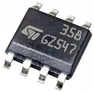
THS4031 - 100MHz 1.6nV Low-Noise Op Amp | Texas Instruments
MPN: THS4031 ✓ Active| Qty | Unit Price | Extended |
|---|---|---|
| 1 | $3.2 | $3.20 |
| 10 | $2.88 | $28.80 |
| 100 | $2.45 | $245.00 |
| 500 | $2.1 | $1,050.00 |
| 1,000 | $1.85 | $1,850.00 |
THS4031 Overview
A voltage feedback amplifier is a type of operational amplifier that uses voltage feedback to set closed-loop gain, offering high bandwidth and low distortion. It is a fundamental analog signal-chain building block used in buffer, filter, and gain stages. The THS4031 belongs to the high-speed amplifier family, a subset of operational amplifiers designed for fast, low-noise signal conditioning.
Key features include ultra-low 1.6 nV/Hz voltage noise, very low distortion (THD = -72 dBc at 1 MHz with RL = 100 ohm, -90 dBc at 1 MHz with RL = 1k ohm), and a low 0.5-mV typical input offset voltage. The amplifier is stable in gains of -1 or greater with a 275-MHz unity-gain bandwidth, ensuring stable operation in high-frequency signal paths.
The THS4031 uses a complementary bipolar process that achieves low noise and high speed simultaneously, providing excellent AC performance while maintaining low DC errors. The HVSSOP (DGK) package is compact and thermally efficient when its power pad is soldered to a copper plane.
Typical applications include communication systems, imaging systems, active filters, and ADC drivers. In communication receivers, the 1.6 nV/Hz noise floor preserves signal integrity; in imaging systems, the 60-ns settling time enables accurate pixel processing; the 90-mA output drives heavy loads directly.
Design tip: decouple supplies with 0.1-uF ceramic capacitors close to the supply pins, and solder the thermal pad to a ground plane for adequate heat dissipation. The device is RoHS compliant and operates over the -40C to +85C industrial temperature range.
Drop-in alternatives for THS4031 — same package, pin-to-pin compatible. Different-package parts requiring PCB rework are excluded.
Variants in this series
Same-series models that are drop-in compatible with THS4031 (same form factor and footprint) — differing in Package, THD, Amplifier Type, Bandwidth, Settling Time (0.1%).
Quick Comparison Tool — Select alternative parts for side-by-side comparison:
THS4031Q-Q1
✅ Drop-In✓ In Stock
$1.63 / Unit
View Datasheet →THS4031CDGNR
✅ Drop-In✓ In Stock
$1.62 / Unit
View Datasheet →THS4031ID
✅ Drop-In📋 Reference alternative (not in catalog)
THS4032IDGNR
✅ Drop-In📋 Reference alternative (not in catalog)
THS4011CDGNR
✅ Drop-In ⚠️ Specs Unverified📋 Reference alternative (not in catalog)
THS4031 Maximum Ratings & Electrical Characteristics
| Amplifier Type | Voltage Feedback |
| Number of Channels | 1 |
| Bandwidth | 100 MHz (G=2) |
| Unity-Gain Bandwidth | 275 MHz |
| Slew Rate | 100 V/us |
| Settling Time (0.1%) | 60 ns |
| Voltage Noise | 1.6 nV/Hz |
| Input Offset Voltage | 0.5 mV (typ) |
| THD | -72 dBc at 1 MHz, RL = 100 ohm; -90 dBc at 1 MHz, RL = 1k ohm |
| Output Current | 90 mA |
| Supply Current | 8.5 mA per channel |
| Supply Voltage Range | +/-5 V to +/-15 V |
| Stability | Stable in gains of -1 V/V or greater |
| Operating Temperature | -40C to +85C |
| Package | 8-HVSSOP (DGK) with power pad |
| Mounting Type | Surface Mount |
| RoHS Status | Compliant |
THS4031 Pin Configuration
| Pin 1 | OUT — Amplifier output |
| Pin 2 | -IN — Inverting input |
| Pin 3 | +IN — Non-inverting input |
| Pin 4 | V- — Negative supply |
| Pin 5 | NC — No connection |
| Pin 6 | NC — No connection |
| Pin 7 | V+ — Positive supply |
| Pin 8 | NC — No connection |
| Pin PAD | PowerPAD — Thermal pad - solder to ground plane for heat dissipation |
Typical Applications
THS4031 is suitable for 6 applications: Communications Systems, Imaging Systems, ADC Driver Stage, Active Filters, Test and Measurement Instrumentation, Video and Imaging Buffer.
Communications Systems
In communications receivers and IF/RF signal chains, the THS4031's 1.6 nV/Hz voltage noise preserves SNR for weak signals, while its 100-MHz bandwidth covers wideband IF stages. The amplifier is placed in gain-of-2 or inverting gain stages between mixers and ADCs, with the 100-V/us slew rate handling large-swing modulated carriers without slew-induced distortion. Its 90-mA output drive feeds 50-ohm back-terminated lines directly, eliminating an extra buffer stage and reducing noise contributions in the receive path.
Recommended
Imaging Systems
Ultrasound and medical imaging front-ends benefit from the THS4031's 60-ns settling time to 0.1%, which supports accurate pixel and time-gated processing, and its 1.6 nV/Hz noise floor that preserves echo signal detail from piezo transducers. Operating from +/-5V to +/-15V supplies allows direct interfacing with bipolar transducer signals. The amplifier drives cable and filter loads with its 90-mA output, and its low offset of 0.5 mV typ minimizes baseline drift across scan lines in high-dynamic-range imaging chains.
Recommended
ADC Driver Stage
As an ADC driver, the THS4031 settles to 0.1% in 60 ns and produces only -90 dBc distortion at 1 MHz into 1k ohm, preserving SFDR for 12- to 16-bit converters. Placed directly before the ADC input in inverting or gain-of-2 configuration, its 90-mA output drives the ADC's dynamic input charge injection. Supplying the device from +/-5V keeps output swing compatible with unipolar ADC input ranges via level shifting, and the low 1.6 nV/Hz noise does not degrade the converter's noise floor at typical closed-loop gains.
Recommended
Active Filters
The THS4031's 275-MHz unity-gain bandwidth and stability in gains of -1 or greater make it ideal for high-frequency multiple-feedback and Sallen-Key active filters in the 1- to 20-MHz range. Its 1.6 nV/Hz noise contributes minimal noise gain to the filter passband, and its low offset (0.5 mV typ) keeps DC accuracy in DC-coupled topologies. The amplifier's flat bandwidth at moderate gains preserves the intended filter Q and cutoff frequency, while the DGK power pad ensures a low-impedance ground that prevents high-frequency ground loops.
Recommended
Test and Measurement Instrumentation
Bench instruments, scopes front-ends, and signal generators use the THS4031 as a low-noise gain stage where its -72 dBc THD at 1 MHz keeps harmonics below measurement resolution. The 100-V/us slew rate reproduces fast edges without distortion, and the +/-15V supply operation provides generous output swing for driving attenuators and coaxial lines through 50-ohm back-termination. Its 8.5-mA quiescent current per channel keeps instrument internal power budgets manageable while delivering lab-grade signal fidelity across the -40C to +85C operating range.
Recommended
Video and Imaging Buffer
The THS4031 buffers video and high-speed imaging signals where its 60-ns settling and 100-V/us slew rate support standard and high-resolution video bandwidths with minimal differential gain and phase error. Used in a gain-of-2 configuration to drive back-terminated 75-ohm or 50-ohm coaxial cable, its 90-mA output capability maintains signal amplitude into heavy loads. The low input offset of 0.5 mV typ avoids visible brightness shifts, and the compact 8-pin HVSSOP (DGK) package fits dense multiplexed video routing boards.
Recommended
Recommended Products Summary
Engineering reference data for THS4031 — comparison, design guidance, and compliance information.
Selection Guide
Comparison with Alternatives
| Parameter | This Product | THS4031Q-Q1 | THS4031CDGNR | THS4032IDGNR |
|---|---|---|---|---|
| Package | 8-HVSSOP (DGK) | 8-HVSSOP (DGK) - same | 8-HVSSOP (DGK) - same | 8-HVSSOP (DGK) - same |
| Brand | Texas Instruments | Texas Instruments | Texas Instruments | Texas Instruments |
| Channels | 1 | 1 | 1 | 2 |
| Bandwidth | 100 MHz (G=2) | 100 MHz | 100 MHz | 100 MHz |
| Voltage Noise | 1.6 nV/Hz | 1.6 nV/Hz | 1.6 nV/Hz | 1.6 nV/Hz |
| Slew Rate | 100 V/us | 100 V/us | 100 V/us | 100 V/us |
| Supply Current | 8.5 mA/ch | 8.5 mA/ch | 8.5 mA/ch | 8.5 mA/ch (x2) |
| Temperature Range | -40C to +85C | -40C to +125C (automotive) | 0C to +70C | -40C to +85C |
| AEC-Q100 | Not qualified | Qualified | Not qualified | Not qualified |
Key Differentiators
- Ultra-low 1.6 nV/Hz voltage noise (vs THS4011CDGNR)
- Automotive-grade drop-in option (vs THS4031Q-Q1)
- Low power per channel (vs THS4032IDGNR)
Design Notes
Solder the HVSSOP (DGK) PowerPAD to a contiguous copper ground plane. The pad is not optional - it provides the primary thermal path and a low-inductance ground connection essential for the 275-MHz unity-gain bandwidth. Per the TI THS403x datasheet, use a 4x4 via array (or more) under the pad tied to the ground plane to minimize thermal resistance and prevent high-frequency ground bounce.
Decouple both supplies with 0.1-uF ceramic capacitors placed within 2 mm of the V+ (pin 7) and V- (pin 4) pins, plus 2.2-uF or 6.8-uF bulk tantalum capacitors per supply rail. At +/-15V supplies, keep total dissipation in mind: 8.5 mA quiescent plus load current through the headroom. Poor decoupling at high frequency causes peaking and potential oscillation at unity-gain-critical gains.
The THS4031 is stable only in gains of -1 V/V or greater (noise gain >= 2). Using it as a pure unity-gain follower with low feedback resistance may cause instability. Use feedback resistors in the several-hundred-ohm to few-kilohm range - too large a value interacts with input capacitance and adds noise; too small overloads the output stage. Source: TI THS403x datasheet application section.
Compliance Information
RoHS compliant per TI product page and internal database. AEC-Q100 not applicable to standard grade - use THS4031Q-Q1 for automotive qualification.