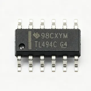
TPS54360QDDARQ1 - 60V 3.5A Buck Converter | Texas Instruments
MPN: TPS54360QDDARQ1 ✓ Active| Qty | Unit Price | Extended |
|---|---|---|
| 1 | $4.1 | $4.10 |
| 10 | $3.7 | $37.00 |
| 100 | $3.2 | $320.00 |
| 500 | $2.8 | $1,400.00 |
| 1,000 | $2.45 | $2,450.00 |
Drop-in alternatives for TPS54360QDDARQ1 — same package, pin-to-pin compatible. Different-package parts requiring PCB rework are excluded.
Quick Comparison Tool — Select alternative parts for side-by-side comparison:
TPS54360DDAR
✅ Drop-In✓ In Stock
$1.6 / Unit
View Datasheet →TPS54360BQDDARQ1
✅ Drop-In📋 Reference alternative (not in catalog)
TPS54560QDDARQ1
✅ Drop-In📋 Reference alternative (not in catalog)
TPS5450QDDARQ1
✅ Drop-In✓ In Stock
$2.45 / Unit
View Datasheet →TPS5430QDDARQ1
✅ Drop-In✓ In Stock
$1.95 / Unit
View Datasheet →TPS54360QDDARQ1 Maximum Ratings & Electrical Characteristics
| Topology | Buck (Step-Down) |
| Input Voltage Range | 4.5 V to 60 V |
| Output Voltage Range | 0.8 V adjustable upward |
| Maximum Output Current | 3.5 A |
| Number of Outputs | 1 |
| Load Dump Survivability | 65 V per ISO 7637 |
| Control Topology | Current Mode |
| Light-Load Mode | Eco-mode pulse-skip (low ripple) |
| Operating Temperature | -40C to +125C |
| Package | 8-PowerSOIC (DDA, SO-8 PowerPAD, 3.90mm width) |
| Mounting Type | Surface Mount |
| Qualification | AEC-Q100 (Automotive Q1) |
| Integrated FET | High-side MOSFET integrated |
| RoHS Status | [DATA_NEEDED: RoHS status] |
| Switching Frequency | [DATA_NEEDED: switching frequency] |
TPS54360QDDARQ1 Pin Configuration
| Pin 1 | BOOT — Bootstrap capacitor connection for high-side gate driver |
| Pin 2 | VIN — Input supply, 4.5V to 60V |
| Pin 3 | EN/UVLO — Enable and adjustable undervoltage lockout |
| Pin 4 | SS/TR — Soft-start / tracking control |
| Pin 5 | VSENSE — Feedback voltage sense for output regulation |
| Pin 6 | COMP — Error amplifier output for loop compensation |
| Pin 7 | GND — Ground reference |
| Pin 8 | PH — Phase (switch node) connection to inductor |
| Pin Pad | PowerPAD — Exposed thermal pad, must be soldered to grounded copper for thermal and electrical performance |
Safe Operating Area (SOA) & Thermal Characteristics
No official SOA curve available for this component. Always operate within absolute maximum ratings specified in the datasheet. Ensure adequate cooling and derate as needed.
Typical Applications
TPS54360QDDARQ1 is suitable for 6 applications: Automotive Battery-Direct Power Rails, 24V Industrial Bus Point-of-Load Conversion, Automotive Infotainment and Cluster Supplies, Motor Drive and Actuator Logic Supplies, Body Electronics and Lighting Modules, Telematics and Connectivity Modules.
Automotive Battery-Direct Power Rails
The TPS54360QDDARQ1 connects directly to 12V automotive battery rails because its 4.5V to 60V input range absorbs cold-crank down to 4.5V and load-dump transients up to 65V per ISO 7637 without external TVS sacrifice. Placed as the first-stage buck feeding downstream 5V or 3.3V point-of-load regulators, its integrated 60V high-side MOSFET and current-mode control deliver 3.5A with simple compensation. AEC-Q100 qualification and -40C to +125C rating remove the need for additional screening in automotive programs.
Recommended
24V Industrial Bus Point-of-Load Conversion
For 24V industrial control buses, the TPS54360QDDARQ1 provides headroom well above nominal rail levels while its Eco-mode pulse-skip maintains efficiency at light standby loads typical of always-on automation nodes. The 3.5A capability supports motor-control logic, sensor hubs, and communication modules. Current-mode control with external compensation lets engineers tune transient response to the load, and the SO-8 PowerPAD dissipates heat through a small PCB copper area, keeping the power stage compact inside DIN-rail and panel enclosures.
Recommended
Automotive Infotainment and Cluster Supplies
Infotainment head units and instrument clusters require clean, sequenced rails from battery input; the TPS54360QDDARQ1 serves as the primary wide-input buck generating a 5V intermediate rail from which audio amplifiers and display supplies derive power. Its 65V load-dump survivability protects the system during alternator transients, and its soft-start pin enables controlled power-up sequencing. With up to 3.5A continuous output, it directly powers display backlights and connectivity modules while Eco-mode limits idle drain when the vehicle is off.
Recommended
Motor Drive and Actuator Logic Supplies
Automotive and industrial motor drivers require robust local rails tolerant of inductive kickback and supply transients. The TPS54360QDDARQ1, with its 60V input and ISO 7637 pulse survivability, converts battery or 24V bus power into regulated logic rails for gate drivers and microcontrollers. Its current-mode architecture rejects input disturbance quickly, which matters when inductive loads cause bus droop. Pairing it with isolated gate drivers on the same board yields a complete compact motor-node power solution rated for harsh environments.
Recommended
Body Electronics and Lighting Modules
Body control modules, LED headlamp drivers, and lighting ECUs are wired directly to battery, facing load dump and jump-start events. The TPS54360QDDARQ1 delivers a regulated front-end for these modules, its Eco-mode cutting quiescent losses to protect battery state of charge. The -40C to +125C ambient range covers underhood and exterior lamp positions, and the AEC-Q1 qualification simplifies automotive customer approval. Its 3.5A output also directly feeds LED string regulation circuitry in mid-power lighting applications.
Recommended
Telematics and Connectivity Modules
Telematics units, gateways, and wireless modules must remain powered during engine crank where battery voltage dips toward 4.5V; the TPS54360QDDARQ1 maintains regulation across this window. With 3.5A available, it powers application processors and RF modules concurrently. The wide 60V tolerance also accommodates miswired or over-voltage input conditions common in field installations. Compact SO-8 PowerPAD packaging suits space-constrained telematics dongles, and Eco-mode reduces standby current for always-connected vehicle nodes.
Recommended
Recommended Products Summary
Engineering reference data for TPS54360QDDARQ1 — comparison, design guidance, and compliance information.
Selection Guide
Comparison with Alternatives
| Parameter | This Product | TPS54360DDAR | TPS54360BQDDARQ1 | TPS54560QDDARQ1 | TPS5450QDDARQ1 | TPS5430QDDARQ1 |
|---|---|---|---|---|---|---|
| Package | SO-8 PowerPAD (DDA) | SO-8 PowerPAD (DDA) - same | SO-8 PowerPAD (DDA) - same | SO-8 PowerPAD (DDA) - same | SO-8 PowerPAD (DDA) - same | SO-8 PowerPAD (DDA) - same |
| Brand | Texas Instruments | Texas Instruments | Texas Instruments | Texas Instruments | Texas Instruments | Texas Instruments |
| Input Voltage Range | 4.5 V to 60 V | 4.5 V to 60 V | 4.5 V to 60 V | 4.5 V to 60 V | [DATA_NEEDED] | [DATA_NEEDED] |
| Output Current | 3.5 A | 3.5 A | 3.5 A | 5 A | 5 A | 3 A |
| AEC-Q100 Qualification | Qualified (Q1) | Not qualified | Qualified (Q1) | Qualified (Q1) | Qualified (Q1) | Qualified (Q1) |
| Light-Load Eco-mode | Yes (pulse-skip) | Yes (pulse-skip) | Yes (pulse-skip) | Yes | [DATA_NEEDED] | [DATA_NEEDED] |
| Load Dump Survivability | 65 V per ISO 7637 | 65 V per ISO 7637 | 65 V per ISO 7637 | [DATA_NEEDED] | [DATA_NEEDED] | [DATA_NEEDED] |
| Typical Price (1 pc, as of 2026-08-29) | $4.10 | [DATA_NEEDED] | [DATA_NEEDED] | [DATA_NEEDED] | [DATA_NEEDED] | [DATA_NEEDED] |
Key Differentiators
- Automotive AEC-Q1 qualification (vs TPS54360DDAR)
- Higher current headroom available in same footprint (vs TPS54560QDDARQ1)
- Superior input transient robustness (vs TPS5430QDDARQ1)
Design Notes
The SO-8 PowerPAD exposed pad is the primary thermal path. Solder it to a grounded copper pour of at least 2x2 via-stitched area; without adequate PowerPAD connection the device cannot sustain 3.5A continuous output at elevated ambient temperatures. Follow the TI datasheet thermal design section when operating above ~2W dissipation.
Place the input decoupling capacitor as close as possible between VIN and GND to minimize high-frequency loop area, and keep the PH-to-inductor-to-output-capacitor loop compact. Use a solid ground plane referenced by the PowerPAD. Route the VSENSE feedback trace away from the PH switch node to avoid injecting switching noise into the error amplifier.
Select an inductor with saturation current above the 3.5A peak current limit, not merely the average load. Do not exceed 60V continuous input; although the device survives 65V ISO 7637 pulses, sustained over-voltage damages the integrated FET. Use the EN/UVLO divider to disable operation below safe battery levels during cold crank.
Compliance Information
AEC-Q100 automotive qualification confirmed by Q1 suffix per TI product page. RoHS/REACH status to be confirmed on TI quality documentation.