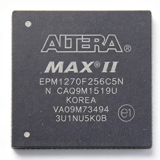
EPM1270F256C5N - MAX II 980-Macrocell CPLD | Intel | Altera
MPN: EPM1270F256C5N ✓ Active| Qty | Unit Price | Extended |
|---|---|---|
| 1 | $28.5 | $28.50 |
| 10 | $24.95 | $249.50 |
| 100 | $21.4 | $2,140.00 |
| 500 | $18.75 | $9,375.00 |
| 1,000 | $16.2 | $16,200.00 |
EPM1270F256C5N Overview
A CPLD (Complex Programmable Logic Device) is a non-volatile programmable logic IC that combines AND/OR array-based macrocell architecture with on-chip flash configuration memory, providing instant-on behavior at power-up without an external boot ROM. Within the broader programmable logic hierarchy, CPLDs sit between small SPLDs/GALs and larger FPGAs, and are widely used as glue logic, I/O expanders, bus interface bridges, and power-up sequencers. MAX II CPLDs added low power consumption (multi-core architecture with internal flash) and integrated features such as user flash memory and a JTAG-based programming interface, making them a preferred choice for cost-sensitive control plane logic.
Key features of the EPM1270F256C5N include non-volatile flash configuration for instant-on operation (no boot PROM required), 8 Kbits of user flash memory (per MAX II family), a JTAG-compliant IEEE 1149.1 boundary-scan / ISP interface, multi-voltage I/O support, and a chip-wide DEV_OE output enable pin. Multi-core architecture distributes logic across four logic regions, simplifying place-and-route for designs targeting fast pin-to-pin timing.
Typical applications include I/O expansion and glue logic in 3.3 V and 2.5 V mixed-voltage systems, power-up sequencing for FPGAs and processors, JTAG-controlled bus bridges, address decoding for memory subsystems, and logic replacement for discrete 74-series TTL/MSI gates. The 256-FBGA package exposes 212 user I/O, allowing direct fan-out for dense parallel buses without external transceivers.
When designing with this device, allocate sufficient PCB area for the 256-ball 1.0 mm pitch FBGA and follow Intel/Altera's reflow profile for lead-free BGA assembly. Use Quartus II software for HDL entry, synthesis, fitting, and timing closure; the same design can be retargeted across other MAX II family members with the same 256-pin footprint, simplifying board reuse.
This page synthesizes distributor pricing, drop-in alternatives, and practical design notes not found in the manufacturer datasheet.
Drop-in alternatives for EPM1270F256C5N — same package, pin-to-pin compatible. Different-package parts requiring PCB rework are excluded.
Variants in this series
Same-series models that are drop-in compatible with EPM1270F256C5N (same form factor and footprint) — differing in Package, Programming Interface, Process Technology, RoHS Status, Operating Temperature.
Quick Comparison Tool — Select alternative parts for side-by-side comparison:
EPM1270F256C5
✓ In Stock
$25.4 / Unit
View Datasheet →EPM1270T144I5N
✓ In Stock
$23.4 / Unit
View Datasheet →EPM1270F256
✓ In Stock
$10.85 / Unit
View Datasheet →EPM1270GF256C5N
📋 Reference alternative (not in catalog)
EPM1270F256C4N
📋 Reference alternative (not in catalog)
EPM1270GF256C4
📋 Reference alternative (not in catalog)
EPM1270F256C5N Maximum Ratings & Electrical Characteristics
| Series | MAX II |
| Family | EPM1270 |
| Device Type | CPLD (Complex Programmable Logic Device) |
| Number of Macrocells | 980 |
| Number of Logic Elements | 1270 |
| Number of User I/O | 212 |
| Propagation Delay (tPD) | 6.2 ns |
| Maximum Frequency (fMAX) | 201.1 MHz |
| Supply Voltage - Internal | 2.5 V / 3.3 V |
| Operating Temperature | 0°C to 85°C (TJ) |
| Mounting Type | Surface Mount |
| Package / Case | 256-FBGA (256-BGA) |
| Supplier Device Package | 256-FBGA |
| Process Technology | 0.18 µm |
| Programmable Type | Non-volatile flash, in-system programmable |
| Programming Interface | JTAG (IEEE 1149.1) / ISP |
| RoHS Status | Details (per distributor product page) |
EPM1270F256C5N 256-fbga Pin Configuration Guide
Pin configuration for EPM1270F256C5N (256-fbga package). This digital IC includes GPIO, communication interfaces (UART, SPI, I2C), and power pins. Refer to the manufacturer datasheet for alternate pin functions and configuration options. Essential for embedded system design and PCB layout.

No detailed pinout data available for EPM1270F256C5N.
Refer to the datasheet for full pin configuration.
Typical Applications
EPM1270F256C5N is suitable for 6 applications: I/O Expansion and Glue Logic, Power-Up Sequencing and Reset Management, JTAG-Controlled Bus Bridges, Address Decoding for Memory Subsystems, Replacing Discrete TTL/MSI Logic, Industrial Control and Interface Logic.
I/O Expansion and Glue Logic
The EPM1270F256C5N fits I/O expansion and glue logic because its 212 user I/O pins and 980 macrocells provide ample density to replace dozens of 74-series TTL gates while consuming a single BGA footprint. Its 6.2 ns pin-to-pin delay and 201.1 MHz fMAX support synchronous interfaces such as SPI, I2C, and parallel memory buses running at tens of MHz. The non-volatile flash configuration means the device powers up with the glue logic active - no external boot ROM is required - which simplifies board design and reduces BOM. Unlike a small FPGA, the CPLD's instant-on behavior is deterministic and free from bitstream load latency, making it ideal for control plane logic that must be ready before the host processor boots.
Recommended
Power-Up Sequencing and Reset Management
The EPM1270F256C5N is well suited to multi-rail power-up sequencing because each macrocell can drive a discrete enable signal with deterministic timing - no firmware or boot ROM is required. Its 980 macrocells can generate dozens of sequenced enables for FPGA, ASIC, and processor rails, with each transition timed by internal logic rather than analog delay lines. The 2.5 V / 3.3 V internal supply lets the CPLD operate directly from a 3.3 V standby rail while monitoring higher-voltage rails through its user I/O banks. Compared to a sequencer IC, the CPLD offers full design flexibility - sequencing order, delays, and fault responses are HDL-defined rather than resistor-set.
Recommended
JTAG-Controlled Bus Bridges
The EPM1270F256C5N implements JTAG-controlled bus bridges because its 980 macrocells can mux and translate between SPI, I2C, UART, and parallel buses while the JTAG port is repurposed for in-system configuration and boundary-scan test. The chip-wide DEV_OE pin provides synchronous output enable for all 212 user I/O - useful for tri-state bus isolation during programming or test. Its instant-on non-volatile configuration means the bridge is active immediately at power-up without waiting for an MCU or FPGA to load. Engineers typically pair this CPLD with an MCU running custom firmware on the far side of the bridge, using the CPLD as the deterministic protocol translator.
Recommended
Address Decoding for Memory Subsystems
The EPM1270F256C5N addresses memory subsystems because its 6.2 ns pin-to-pin delay and 201.1 MHz fMAX easily decode asynchronous memory cycles at 100 MHz+ with comfortable timing margin. The 212 user I/O accept wide address buses (24+ bits) plus chip-select fan-out for SRAM, NOR flash, and peripheral registers without external buffers. Compared to discrete 74-series decoders, the CPLD integrates multiple decode maps into one device - boot ROM, peripheral, and external bus maps can all be implemented in one 256-FBGA part. The non-volatile flash configuration means the decode map is fixed at silicon level - no risk of inadvertent reprogramming in the field.
Recommended
Replacing Discrete TTL/MSI Logic
The EPM1270F256C5N replaces discrete TTL/MSI logic because 980 macrocells can absorb hundreds of AND/OR/NAND/flip-flop gates into one BGA, reducing PCB area, BOM count, and assembly cost. Its multi-core architecture with four logic regions fits wide combinational paths without place-and-route congestion. Power consumption is typically lower than the equivalent TTL gate count because internal macros switch at lower capacitance per transition. Engineers migrating legacy 74F/74AS/74LS designs to a CPLD gain design security (the JEDEC map is locked in flash) and board simplification (one BGA replaces dozens of SOIC parts).
Recommended
Industrial Control and Interface Logic
The EPM1270F256C5N fits industrial control designs because its 212 user I/O drive the wide parallel buses and discrete I/O typical of PLC backplanes and motor-control interface boards. The 0°C to 85°C commercial operating junction temperature range covers most indoor industrial enclosures; for harsher environments, the EPM1270T144I5N industrial variant (-40°C to 100°C) in TQFP-144 is the same die in a different package. The CPLD's deterministic 6.2 ns pin-to-pin delay simplifies worst-case interrupt latency calculations in safety-related logic. Compared to an FPGA, the instant-on non-volatile behavior eliminates bitstream load delay, which is critical for fast-startup industrial controllers.
Recommended
Recommended Products Summary
Engineering reference data for EPM1270F256C5N — comparison, design guidance, and compliance information.
Selection Guide
Comparison with Alternatives
| Parameter | This Product | EPM1270GF256C5N | EPM1270F256C5 | EPM1270F256C4N | EPM1270GF256C4 | EPM1270F256 | EPM1270T144I5N |
|---|---|---|---|---|---|---|---|
| Brand | Altera / Intel | Altera / Intel | Altera / Intel | Altera / Intel | Altera / Intel | Altera / Intel | Altera / Intel |
| Package | 256-FBGA | 256-FBGA - same | 256-FBGA - same | 256-FBGA - same | 256-FBGA - same | 256-FBGA - same | TQFP-144 - different |
| Macrocells | 980 | 980 | 980 | 980 | 980 | 980 | 980 |
| Logic Elements | 1270 | 1270 | 1270 | 1270 | 1270 | 1270 | 1270 |
| User I/O | 212 | 212 | 212 | 212 | 212 | 212 | Data not specified for TQFP-144 variant |
| Pin-to-Pin Delay (tPD) | 6.2 ns | 6.2 ns (C5 grade) | 6.2 ns (C5 grade) | approx 7.5 ns (C4 grade) | approx 7.5 ns (C4 grade) | Speed grade as marked | approx 5.0 ns (I5 industrial grade) |
| Max Internal Frequency (fMAX) | 201.1 MHz | 201.1 MHz | 201.1 MHz | approx 152 MHz (C4 grade) | approx 152 MHz (C4 grade) | Speed grade as marked | approx 304 MHz (I5 grade) |
| Internal Supply Voltage | 2.5 V / 3.3 V | 1.8 V / 2.5 V / 3.3 V (MAX II G) | 2.5 V / 3.3 V | 2.5 V / 3.3 V | 1.8 V / 2.5 V / 3.3 V (MAX II G) | 2.5 V / 3.3 V | 2.5 V / 3.3 V |
| Operating Temperature | 0°C to 85°C (TJ) | 0°C to 85°C (TJ) | 0°C to 85°C (TJ) | 0°C to 85°C (TJ) | 0°C to 85°C (TJ) | 0°C to 85°C (TJ) | -40°C to 100°C (industrial TJ) |
| Lead-Free Finish | Yes (N suffix) | Yes | No (lead-based) | Yes | No (lead-based) | As marked | Yes |
Key Differentiators
- Same 256-FBGA footprint across C4 and C5 speed grades (vs EPM1270F256C4N)
- MAX II G variants add 1.8 V core option (vs EPM1270GF256C5N)
- Industrial temperature grade in TQFP-144 alternative (vs EPM1270T144I5N)
Design Notes
The 256-FBGA package uses 1.0 mm ball pitch and requires a 4-layer or 6-layer PCB with controlled-impedance traces and a 0.4 mm solder mask opening. Per Intel/Altera application notes, use microvia (laser-drilled) stacked via technology for inner-row fan-out; through-hole vias under the BGA must use a tented-via or via-in-pad process to prevent solder wicking. Allow a keep-out zone of at least 0.5 mm around the BGA for reflow profiling.
The EPM1270F256C5N has separate VCCINT (core) and VCCIO (I/O bank) supply pins. According to the MAX II Device Handbook, all VCCINT pins must be connected to a single 2.5 V or 3.3 V plane with bulk decoupling (one 10 µF tantalum or ceramic per side) and 0.1 µF ceramic caps adjacent to every VCC pin pair. I/O banks can be independently powered at 1.5 V / 1.8 V / 2.5 V / 3.3 V to interface mixed-voltage peripherals; unused VCCIO pins must still be tied to a valid rail.
Do not leave JTAG pins (TDI, TDO, TMS, TCK) floating; they must be pulled to defined logic levels per the MAX II family datasheet to prevent inadvertent boundary-scan or ISP activation. The DEV_OE pin is a chip-wide output enable - leaving it floating can leave outputs in an undefined state at power-up. For multi-voltage designs, confirm the chosen I/O standard is supported in the selected VCCIO bank voltage (see MAX II Device Handbook I/O standard compatibility table).
Compliance Information
RoHS compliant per 'N' suffix and distributor product pages (DigiKey, Mouser, Arrow, Heisener). Not AEC-Q100 qualified (commercial temperature grade only). Halogen-free status not explicitly listed in verified web data.







