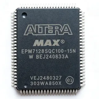
EPM7128SQC100-10 - MAX 7000S CPLD, 128 Macro, 84 I/O | Altera
MPN: EPM7128SQC100-10 ✗ End of Life| Qty | Unit Price | Extended |
|---|---|---|
| 1 | $18.5 | $18.50 |
| 10 | $16.2 | $162.00 |
| 100 | $13.75 | $1,375.00 |
| 500 | $11.4 | $5,700.00 |
| 1,000 | $9.85 | $9,850.00 |
EPM7128SQC100-10 Overview
What is a CPLD? A Complex Programmable Logic Device is a non-volatile, instantly-on programmable logic device that sits between simple PAL/GAL devices and larger FPGAs. It uses an EEPROM- or flash-based architecture to retain configuration without a boot PROM, offers predictable timing with deterministic pin-to-pin delays, and is typically used for glue logic, address decoding, state-machine control, and bus-interface bridging. Within the programmable-logic hierarchy (PAL/GAL < CPLD < FPGA), the MAX 7000S family represents a mature, cost-effective tier for 5V systems.
Key features include a 100 MHz maximum operating frequency, in-system programmability (ISP) via JTAG, programmable macrocell flipflops with individual clear, preset, clock, and clock-enable controls, open-drain output option, and pin compatibility with the wider MAX 7000S family. The device supports 5V core and I/O operation, with I/O pins tolerant of mixed-voltage interfacing.
The EPM7128SQC100-10 uses a second-generation MAX architecture with a global interconnect fabric linking 16 Logic Array Blocks (LABs), each containing 8 macrocells. This architecture delivers fast, deterministic propagation delays that are critical for synchronous designs where setup/hold margins must be calculated precisely. The 100-pin PQFP package provides a low-cost, easy-to-inspect footprint for through-hole-style prototyping and rework.
Typical applications include address decoding and bus interfacing for microprocessors and microcontrollers, glue logic between ASICs and standard peripherals, state-machine control in industrial controllers, legacy 5V system upgrades from discrete 74LS/74HC logic, and peripheral expansion for legacy parallel-port designs. Designers also use the EPM7128 family for I/O voltage translation and timing adjustment in mixed-voltage boards.
When designing with this part, treat the 10 ns speed grade as the timing baseline: any design migrated from a faster grade (e.g., -6 or -7) must be re-checked for setup/hold at the new tPD. Decoupling requires 0.1 uF and 10 uF bulk caps near VCC pins, and unused JTAG TCK pins should be tied to GND through 1 kohm in noisy environments.
This page synthesizes distributor pricing, drop-in alternatives (EPM7128SQC100-7, EPM7128SQC100-15N, EPM7128SQC100-10N), and practical design notes not found in the manufacturer datasheet alone, helping engineers shorten the selection and qualification cycle for legacy and 5V-tolerant designs.
Drop-in alternatives for EPM7128SQC100-10 — same package, pin-to-pin compatible. Different-package parts requiring PCB rework are excluded.
Variants in this series
Same-series models that are drop-in compatible with EPM7128SQC100-10 (same form factor and footprint) — differing in Package, Operating Temperature, Logic Array Blocks (LABs), Propagation Delay (tPD), Supply Voltage (VCCINT).
Quick Comparison Tool — Select alternative parts for side-by-side comparison:
EPM7128SQC100-7
✅ Drop-In✓ In Stock
$10.85 / Unit
View Datasheet →EPM7128SQC100-15N
✅ Drop-In📋 Reference alternative (not in catalog)
EPM7128SQC100-10N
✅ Drop-In✓ In Stock
$14.95 / Unit
View Datasheet →EPM7128SQC100-6
✅ Drop-In✓ In Stock
$7.1 / Unit
View Datasheet →EPM7128AETC100-10
✅ Drop-In✓ In Stock
$13.85 / Unit
View Datasheet →EPM7128SQC100-10 Maximum Ratings & Electrical Characteristics
| Family | MAX 7000S |
| Device Type | CPLD (Complex Programmable Logic Device) |
| Macro Cells | 128 |
| Logic Elements / Gates | 2,500 usable gates |
| Maximum User I/O | 84 |
| Logic Array Blocks (LABs) | 16 |
| Maximum Operating Frequency | 100 MHz |
| Pin-to-Pin Logic Delay (tPD) | 10 ns |
| Supply Voltage | 5 V |
| Process Technology | 5V CMOS, EEPROM-based |
| Programmability | In-System Programmable (ISP) via JTAG |
| Package | 100-pin PQFP (Plastic Quad Flat Pack) |
| Operating Temperature | 0C to +70C (commercial) |
| Mounting Type | Surface Mount |
EPM7128SQC100-10 Pin Configuration
| Pin 1 | I/O — User I/O pin (macrocell-assignable) |
| Pin 2 | I/O — User I/O pin |
| Pin 3 | I/O — User I/O pin |
| Pin 4 | I/O — User I/O pin |
| Pin 5 | I/O — User I/O pin |
| Pin 6 | GND — Ground |
| Pin 7 | I/O — User I/O pin |
| Pin 8 | I/O — User I/O pin |
| Pin 9 | I/O — User I/O pin |
| Pin 10 | I/O — User I/O pin |
| Pin 11 | I/O — User I/O pin |
| Pin 12 | I/O — User I/O pin |
| Pin 13 | I/O — User I/O pin |
| Pin 14 | I/O — User I/O pin |
| Pin 15 | VCC — +5V supply |
| Pin 16 | I/O — User I/O pin |
| Pin 17 | I/O — User I/O pin |
| Pin 18 | I/O — User I/O pin |
| Pin 19 | I/O — User I/O pin |
| Pin 20 | I/O — User I/O pin |
| Pin 21 | I/O — User I/O pin |
| Pin 22 | I/O — User I/O pin |
| Pin 23 | I/O — User I/O pin |
| Pin 24 | GND — Ground |
| Pin 25 | I/O — User I/O pin |
| Pin 26 | I/O — User I/O pin |
| Pin 27 | I/O — User I/O pin |
| Pin 28 | I/O — User I/O pin |
| Pin 29 | I/O — User I/O pin |
| Pin 30 | I/O — User I/O pin |
| Pin 31 | TDI — JTAG Test Data In |
| Pin 32 | TMS — JTAG Test Mode Select |
| Pin 33 | TCK — JTAG Test Clock |
| Pin 34 | TDO — JTAG Test Data Out |
| Pin 35 | I/O — User I/O pin |
| Pin 36 | I/O — User I/O pin |
| Pin 37 | I/O — User I/O pin |
| Pin 38 | I/O — User I/O pin |
| Pin 39 | I/O — User I/O pin |
| Pin 40 | VCC — +5V supply |
| Pin 41 | I/O — User I/O pin |
| Pin 42 | I/O — User I/O pin |
| Pin 43 | I/O — User I/O pin |
| Pin 44 | I/O — User I/O pin |
| Pin 45 | I/O — User I/O pin |
| Pin 46 | I/O — User I/O pin |
| Pin 47 | I/O — User I/O pin |
| Pin 48 | GND — Ground |
| Pin 49 | I/O — User I/O pin |
| Pin 50 | I/O — User I/O pin |
| Pin 51 | GNDINT — Ground (internal) |
| Pin 52 | I/O — User I/O pin |
| Pin 53 | I/O — User I/O pin |
| Pin 54 | I/O — User I/O pin |
| Pin 55 | I/O — User I/O pin |
| Pin 56 | I/O — User I/O pin |
| Pin 57 | I/O — User I/O pin |
| Pin 58 | I/O — User I/O pin |
| Pin 59 | I/O — User I/O pin |
| Pin 60 | I/O — User I/O pin |
| Pin 61 | I/O — User I/O pin |
| Pin 62 | I/O — User I/O pin |
| Pin 63 | GND — Ground |
| Pin 64 | I/O — User I/O pin |
| Pin 65 | I/O — User I/O pin |
| Pin 66 | I/O — User I/O pin |
| Pin 67 | I/O — User I/O pin |
| Pin 68 | I/O — User I/O pin |
| Pin 69 | I/O — User I/O pin |
| Pin 70 | I/O — User I/O pin |
| Pin 71 | I/O — User I/O pin |
| Pin 72 | VCC — +5V supply |
| Pin 73 | I/O — User I/O pin |
| Pin 74 | I/O — User I/O pin |
| Pin 75 | I/O — User I/O pin |
| Pin 76 | I/O — User I/O pin |
| Pin 77 | I/O — User I/O pin |
| Pin 78 | I/O — User I/O pin |
| Pin 79 | I/O — User I/O pin |
| Pin 80 | I/O — User I/O pin |
| Pin 81 | I/O — User I/O pin |
| Pin 82 | I/O — User I/O pin |
| Pin 83 | GND — Ground |
| Pin 84 | I/O — User I/O pin |
| Pin 85 | I/O — User I/O pin |
| Pin 86 | I/O — User I/O pin |
| Pin 87 | I/O — User I/O pin |
| Pin 88 | I/O — User I/O pin |
| Pin 89 | I/O — User I/O pin |
| Pin 90 | I/O — User I/O pin |
| Pin 91 | I/O — User I/O pin |
| Pin 92 | I/O — User I/O pin |
| Pin 93 | I/O — User I/O pin |
| Pin 94 | I/O — User I/O pin |
| Pin 95 | I/O — User I/O pin |
| Pin 96 | VCC — +5V supply |
| Pin 97 | I/O — User I/O pin |
| Pin 98 | I/O — User I/O pin |
| Pin 99 | I/O — User I/O pin |
| Pin 100 | I/O — User I/O pin |
Typical Applications
EPM7128SQC100-10 is suitable for 6 applications: Microprocessor Address Decoding, Bus Interface Bridging (ISA / PCI / VME), Industrial Glue Logic Replacement, State Machine Control, Legacy Peripheral Expansion, I/O Voltage Translation and Level Shifting.
Microprocessor Address Decoding
The EPM7128SQC100-10 is well-suited for address decoding in 8/16/32-bit microprocessor systems, where its 128 macrocells and 84 I/O pins allow multiple chip-select and wait-state signals to be generated from a single device. With a deterministic 10 ns pin-to-pin delay, the CPLD can decode an address bus in real time without inserting wait states, making it ideal for 8086, 68000, and legacy ARM7 designs. The wide 5V I/O tolerance also allows direct interface to classic TTL/CMOS logic levels. Power dissipation is low at typical clock rates (estimated: <500 mW active), so no special thermal management is needed.
Recommended
Bus Interface Bridging (ISA / PCI / VME)
With 100 MHz maximum frequency and 10 ns tPD, the EPM7128SQC100-10 acts as a fast bus-interface bridge between legacy 5V buses (ISA, VME) and 3.3V peripherals. The 128 macrocells can implement FIFOs, byte-swapping logic, and interrupt steering in a single chip, reducing BOM count versus discrete 74LS glue logic. Open-drain output option supports wired-OR bus arbitration. Estimated power dissipation under full I/O toggle at 50 MHz is around 750 mW; 0.1 uF + 10 uF decoupling near each VCC pin is recommended.
Recommended
Industrial Glue Logic Replacement
The EPM7128SQC100-10 is widely used to consolidate discrete 74LS/74HC/74FTTL gates in industrial controllers, where a single 100-pin PQFP CPLD can replace dozens of discrete logic packages. Its deterministic 10 ns delay enables precise state-machine timing for sequencing pumps, valves, and motor drivers in PLC and process-control applications. The 0-70C commercial temperature range suits cabinet-mounted industrial equipment; for harsher environments, the EPM7128EQC100-15 (industrial grade) is recommended. Estimated BOM savings: 60-80% board area reduction versus discrete TTL.
Recommended
State Machine Control
The 16 LAB architecture of the EPM7128SQC100-10 makes it efficient for implementing complex state machines, including Mealy and Moore machines for protocol converters, encoder/decoder logic, and sequencers. With 128 macrocells, designers can implement 32-64 state FSMs in a single device, far exceeding the capability of small PAL/GAL devices. The deterministic 10 ns tPD ensures predictable state transitions critical for real-time control. The device retains configuration in EEPROM, so state machines power up instantly without boot delays.
Recommended
Legacy Peripheral Expansion
The EPM7128SQC100-10 enables legacy parallel-port and ISA expansion designs by providing reconfigurable I/O and timing logic, extending the life of installed-base peripherals. With 84 user I/O pins, the CPLD can drive parallel printer ports, SCSI interfaces, and custom ISA cards while maintaining 5V TTL compatibility. Designers can re-target the same hardware for different peripherals by reprogramming the EEPROM, avoiding costly board respins. Power is around 500 mW typical at 25 MHz operation, well within legacy supply budgets.
Recommended
I/O Voltage Translation and Level Shifting
The EPM7128SQC100-10 supports 5V-tolerant I/O, allowing it to bridge between 5V legacy systems and 3.3V peripherals without external level shifters. With 84 I/O pins, designers can implement 40+ bidirectional level-shift channels in a single chip. The 10 ns tPD adds minimal latency to translation paths, preserving signal integrity for memory and peripheral interfaces. Designers should consult the MAX 7000 datasheet for absolute maximum ratings on mixed-voltage pins; pull-up resistors on 3.3V sides may be required for open-drain configurations.
Recommended
Recommended Products Summary
Engineering reference data for EPM7128SQC100-10 — comparison, design guidance, and compliance information.
Selection Guide
Comparison with Alternatives
| Parameter | This Product | EPM7128SQC100-7 | EPM7128SQC100-15N | EPM7128SQC100-10N | EPM7128SQC100-6 | EPM7128AETC100-10 |
|---|---|---|---|---|---|---|
| Package | PQFP-100 (QC100) | PQFP-100 (QC100) - same | PQFP-100 (QC100) - same | PQFP-100 (QC100) - same | PQFP-100 (QC100) - same | TQFP-100 - thinner body |
| Brand | Altera (Intel) | Altera (Intel) | Altera (Intel) | Altera (Intel) | Altera (Intel) | Altera (Intel) |
| Macro Cells | 128 | 128 | 128 | 128 | 128 | 128 |
| User I/O | 84 | 84 | 84 | 84 | 84 | 84 |
| Pin-to-Pin Delay (tPD) | 10 ns | 7 ns (faster) | 15 ns (slower) | 10 ns (same) | 6 ns (faster) | 10 ns (same) |
| Supply Voltage | 5 V | 5 V | 5 V | 5 V | 5 V | 3.3 V |
| Family | MAX 7000S | MAX 7000S | MAX 7000S | MAX 7000S | MAX 7000S | MAX 7000A |
Key Differentiators
- Industry-standard 5V CPLD with massive installed base (vs MAX II EPM570T100C5N)
- Drop-in timing upgrade path to faster grades (vs EPM7128SQC100-7)
- Wide package options within MAX 7000S family (vs EPM7128SLC84-10 (PLCC-84))
Design Notes
Estimated: at 5V VCC and 25 MHz operation with 50% I/O toggle, the EPM7128SQC100-10 consumes approximately 500 mW; under full I/O toggle at 100 MHz the figure rises to roughly 750 mW. Decoupling requires 0.1 uF ceramic caps on each VCC pin (pins 15, 40, 72, 96) placed within 5 mm, plus a single 10 uF tantalum bulk cap near the device. Multiple GND pins (6, 24, 48, 63, 83) should each be tied to a low-impedance ground plane for return-current management.
The 100-pin PQFP has a 0.65 mm pitch and is sensitive to solder-bridge defects during reflow. Use a land pattern with solder-mask-defined pads and a 0.15 mm solder paste stencil; for hand prototyping, fine-pitch QFP sockets (e.g., 3M Textool) are recommended. Keep all four VCC pins connected with a power plane or wide traces to share current; place decoupling caps on the same side as the IC, with vias directly to the VCC/GND planes.
Three pitfalls to avoid: (1) Do not leave JTAG TCK floating - tie to GND through 1 kohm if unused to prevent noise-induced state changes; (2) Designs migrated from -7 or -6 grades must be re-checked for setup/hold violations at 10 ns tPD, as the slower grade can break timing closure; (3) The 'N' suffix indicates lead-free / Pb-free termination - the standard EPM7128SQC100-10 has SnPb finish, so verify compatibility with lead-free reflow profiles before substituting.
Compliance Information
EPM7128SQC100-10 (without N suffix) is the standard SnPb finish variant; the EPM7128SQC100-10N is the lead-free / Pb-free termination variant. RoHS/REACH status not confirmed in verified web data - check distributor documentation for the specific lot. AEC-Q100 is not applicable for commercial-temperature CPLDs.