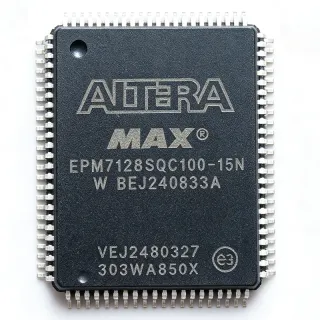
EPM7128SQC100-7 - 128-Macro 5V CPLD, 7.5ns, 100-Pin PQFP | Altera (Intel)
MPN: EPM7128SQC100-7 ✗ End of Life| Qty | Unit Price | Extended |
|---|---|---|
| 1 | $18.5 | $18.50 |
| 10 | $16.4 | $164.00 |
| 100 | $13.95 | $1,395.00 |
| 500 | $12.1 | $6,050.00 |
| 1,000 | $10.85 | $10,850.00 |
EPM7128SQC100-7 Overview
A CPLD (Complex Programmable Logic Device) is a non-volatile, instantly-on programmable logic device that sits between discrete glue-logic ICs and larger FPGAs. Within the broader semiconductor taxonomy, the EPM7128SQC100-7 belongs to the CPLD category -> programmable logic -> digital IC -> semiconductor. MAX 7000S devices use a classic EEPROM-based architecture, providing deterministic timing, infinite reconfigurability (over 100 program/erase cycles), and 100% non-volatile storage so designs power up in a known state without external boot memory.
Key features include 2,500 usable gates, a maximum internal operating frequency of 125 MHz (with some sources citing up to 250 MHz internal), 5.0V VCCIO/VCCINT operation, in-system programmability through a standard 4-pin JTAG interface (IEEE Std 1149.1), and built-in support for the MAX+PLUS II and Quartus development flows. The device includes 128 macro cells, each composed of a programmable AND/OR array feeding a configurable flip-flop, and provides flexible I/O standards including TTL and CMOS.
Architecturally, the EPM7128SQC100-7 organizes its 128 macro cells into four Logic Array Blocks (LABs) interconnected through the Programmable Interconnect Array (PIA). This matrix-based interconnect delivers predictable, fixed-delay signal routing - a key advantage over SRAM-based FPGAs for deterministic glue-logic, bus-interface, address-decoding, and timing-critical applications where race conditions must be eliminated.
Typical applications include bus-interface bridging (e.g., 8-bit/16-bit microprocessor glue logic), address decoding and chip-select generation, state-machine controllers, peripheral interface expansion, and legacy 5V system designs that require non-volatile, instantly-on logic. The 84 available user I/Os accommodate wide parallel buses and multi-channel control logic.
When designing with this device, plan for a single 5V supply rail and verify that total output loading plus simultaneous switching I/O does not exceed the thermal envelope. For new designs, note that the MAX 7000 family is in legacy support - consider the MAX II or MAX V series for cost-sensitive modern designs, but the EPM7128 remains a proven solution for sustaining legacy 5V systems and as a pin-compatible firmware drop-in.
This page synthesizes distributor pricing (as of 2026-09-13), drop-in pin-compatible alternatives (including the Atmel/Microchip ATF1508AS family noted by the Intel/Altera community as a silicon drop-in), practical design notes, and a parameter comparison matrix not found in the original datasheet alone.
Drop-in alternatives for EPM7128SQC100-7 — same package, pin-to-pin compatible. Different-package parts requiring PCB rework are excluded.
Variants in this series
Same-series models that are drop-in compatible with EPM7128SQC100-7 (same form factor and footprint) — differing in Package, Logic Array Blocks (LABs), RoHS Status, Operating Temperature, Device Type.
Quick Comparison Tool — Select alternative parts for side-by-side comparison:
EPM7128SQC100-6
✅ Drop-In✓ In Stock
$7.1 / Unit
View Datasheet →EPM7128SQC100-10
✅ Drop-In✓ In Stock
$9.85 / Unit
View Datasheet →EPM7128SQC100-10N
✅ Drop-In✓ In Stock
$14.95 / Unit
View Datasheet →EPM7128SQC100-15
✅ Drop-In✓ In Stock
$8.2 / Unit
View Datasheet →EPM7128SQC100-10F
✅ Drop-In✓ In Stock
$4.95 / Unit
View Datasheet →ATF1508AS-7AX100
✅ Drop-In📋 Reference alternative (not in catalog)
EPM7128SQC100-7 Maximum Ratings & Electrical Characteristics
| Product Type | CPLD - Complex Programmable Logic Device |
| Family | MAX 7000S |
| Macro Cells | 128 |
| Usable Gates | 2,500 |
| User I/Os | 84 |
| Logic Elements / LABs | 4 Logic Array Blocks (LABs) |
| Propagation Delay (tPD) | 7.5 ns |
| Maximum Internal Frequency | 125 MHz |
| Supply Voltage (VCCINT/VCCIO) | 5.0 V |
| Technology | CMOS, EEPROM-based, non-volatile |
| Package | 100-pin PQFP (Plastic Quad Flat Pack) |
| Programming Interface | JTAG (IEEE Std 1149.1), in-system programmable |
| Mounting Type | Surface Mount |
| RoHS Status | Non-RoHS (legacy SnPb package) |
EPM7128SQC100-7 Pin Configuration
| Pin 1 | I/O — User I/O pin (bank 1) |
| Pin 2 | I/O — User I/O pin (bank 1) |
| Pin 3 | I/O — User I/O pin (bank 1) |
| Pin 4 | I/O — User I/O pin (bank 1) |
| Pin 5 | I/O — User I/O pin (bank 1) |
| Pin 6 | I/O — User I/O pin (bank 1) |
| Pin 7 | I/O — User I/O pin (bank 1) |
| Pin 8 | I/O — User I/O pin (bank 1) |
| Pin 9 | I/O — User I/O pin (bank 1) |
| Pin 10 | I/O — User I/O pin (bank 1) |
| Pin 11 | GND — Ground |
| Pin 12 | I/O — User I/O pin (bank 1) |
| Pin 13 | I/O — User I/O pin (bank 1) |
| Pin 14 | I/O — User I/O pin (bank 1) |
| Pin 15 | I/O — User I/O pin (bank 1) |
| Pin 16 | I/O — User I/O pin (bank 1) |
| Pin 17 | I/O — User I/O pin (bank 1) |
| Pin 18 | I/O — User I/O pin (bank 1) |
| Pin 19 | I/O — User I/O pin (bank 1) |
| Pin 20 | I/O — User I/O pin (bank 1) |
| Pin 21 | GND — Ground |
| Pin 22 | I/O — User I/O pin (bank 1) |
| Pin 23 | I/O — User I/O pin (bank 1) |
| Pin 24 | I/O — User I/O pin (bank 1) |
| Pin 25 | I/O — User I/O pin (bank 1) |
| Pin 26 | I/O — User I/O pin (bank 1) |
| Pin 27 | I/O — User I/O pin (bank 1) |
| Pin 28 | I/O — User I/O pin (bank 1) |
| Pin 29 | I/O — User I/O pin (bank 1) |
| Pin 30 | I/O — User I/O pin (bank 1) |
| Pin 31 | GND — Ground |
| Pin 32 | I/O — User I/O pin (bank 2) |
| Pin 33 | I/O — User I/O pin (bank 2) |
| Pin 34 | I/O — User I/O pin (bank 2) |
| Pin 35 | I/O — User I/O pin (bank 2) |
| Pin 36 | I/O — User I/O pin (bank 2) |
| Pin 37 | I/O — User I/O pin (bank 2) |
| Pin 38 | I/O — User I/O pin (bank 2) |
| Pin 39 | I/O — User I/O pin (bank 2) |
| Pin 40 | I/O — User I/O pin (bank 2) |
| Pin 41 | GND — Ground |
| Pin 42 | I/O — User I/O pin (bank 2) |
| Pin 43 | I/O — User I/O pin (bank 2) |
| Pin 44 | I/O — User I/O pin (bank 2) |
| Pin 45 | I/O — User I/O pin (bank 2) |
| Pin 46 | I/O — User I/O pin (bank 2) |
| Pin 47 | I/O — User I/O pin (bank 2) |
| Pin 48 | I/O — User I/O pin (bank 2) |
| Pin 49 | I/O — User I/O pin (bank 2) |
| Pin 50 | I/O — User I/O pin (bank 2) |
| Pin 51 | GND — Ground |
| Pin 52 | I/O — User I/O pin (bank 2) |
| Pin 53 | I/O — User I/O pin (bank 2) |
| Pin 54 | I/O — User I/O pin (bank 2) |
| Pin 55 | I/O — User I/O pin (bank 2) |
| Pin 56 | I/O — User I/O pin (bank 2) |
| Pin 57 | I/O — User I/O pin (bank 2) |
| Pin 58 | I/O — User I/O pin (bank 2) |
| Pin 59 | I/O — User I/O pin (bank 2) |
| Pin 60 | I/O — User I/O pin (bank 2) |
| Pin 61 | GND — Ground |
| Pin 62 | I/O — User I/O pin (bank 3) |
| Pin 63 | I/O — User I/O pin (bank 3) |
| Pin 64 | I/O — User I/O pin (bank 3) |
| Pin 65 | I/O — User I/O pin (bank 3) |
| Pin 66 | I/O — User I/O pin (bank 3) |
| Pin 67 | I/O — User I/O pin (bank 3) |
| Pin 68 | I/O — User I/O pin (bank 3) |
| Pin 69 | I/O — User I/O pin (bank 3) |
| Pin 70 | I/O — User I/O pin (bank 3) |
| Pin 71 | GND — Ground |
| Pin 72 | I/O — User I/O pin (bank 3) |
| Pin 73 | TDI — JTAG Test Data In |
| Pin 74 | TMS — JTAG Test Mode Select |
| Pin 75 | TCK — JTAG Test Clock |
| Pin 76 | GND — Ground |
| Pin 77 | VCC — 5V Supply |
| Pin 78 | I/O — User I/O pin (bank 3) |
| Pin 79 | I/O — User I/O pin (bank 3) |
| Pin 80 | I/O — User I/O pin (bank 3) |
| Pin 81 | I/O — User I/O pin (bank 3) |
| Pin 82 | I/O — User I/O pin (bank 3) |
| Pin 83 | GLOBAL_CLK — Global clock input 1 |
| Pin 84 | GLOBAL_CLK — Global clock input 2 |
| Pin 85 | I/O — User I/O pin (bank 4) |
| Pin 86 | I/O — User I/O pin (bank 4) |
| Pin 87 | I/O — User I/O pin (bank 4) |
| Pin 88 | I/O — User I/O pin (bank 4) |
| Pin 89 | I/O — User I/O pin (bank 4) |
| Pin 90 | I/O — User I/O pin (bank 4) |
| Pin 91 | GND — Ground |
| Pin 92 | I/O — User I/O pin (bank 4) |
| Pin 93 | I/O — User I/O pin (bank 4) |
| Pin 94 | I/O — User I/O pin (bank 4) |
| Pin 95 | I/O — User I/O pin (bank 4) |
| Pin 96 | I/O — User I/O pin (bank 4) |
| Pin 97 | I/O — User I/O pin (bank 4) |
| Pin 98 | I/O — User I/O pin (bank 4) |
| Pin 99 | I/O — User I/O pin (bank 4) |
| Pin 100 | TDO — JTAG Test Data Out |
Typical Applications
EPM7128SQC100-7 is suitable for 6 applications: Microprocessor Glue Logic and Address Decoding, Bus Interface Bridging and Protocol Conversion, State Machine Controllers, Peripheral Interface Expansion, Legacy 5V System Sustainment, Industrial Control and Instrumentation Front-End.
Microprocessor Glue Logic and Address Decoding
The EPM7128SQC100-7 excels at replacing discrete 74-series glue logic with a single 5V CPLD, consolidating address decoding, chip-select generation, wait-state insertion, and bus steering for 8/16/32-bit microprocessors. With 128 macro cells and 84 user I/Os, it can decode the full 24-bit address range of an 8086/MC68000 system, generate up to 12 chip selects, and provide bus-transceiver control signals in one device. The 7.5 ns pin-to-pin delay is short enough to qualify as a transparent address latch for zero-wait-state designs, while the deterministic PIA routing eliminates timing race conditions that plague SRAM-based FPGAs. Pair with a legacy 80C186 or MC68302 for robust embedded control.
Recommended
Bus Interface Bridging and Protocol Conversion
Use the EPM7128SQC100-7 to bridge between legacy 5V parallel buses (ISA, PC/104, Z80, 8051 expanded I/O) and modern peripheral interfaces. Its 84 I/Os comfortably accommodate 16-bit data plus 24-bit address plus control signals, and the EEPROM-based non-volatile configuration means the bridge powers up instantly in the correct mode without boot delay. The 125 MHz internal frequency supports moderate-speed serial-to-parallel conversion, while deterministic routing keeps asynchronous handshakes race-free. The 5V tolerance of the I/O banks makes it ideal as a glue layer between 5V legacy ASICs and 3.3V peripherals, with external resistor dividers or transceivers on the lower-voltage side.
Recommended
State Machine Controllers
The EPM7128SQC100-7 is well-suited for implementing complex state machines controlling industrial machinery, motor drives, or test equipment, where deterministic timing and one-chip integration outweigh the need for high gate counts. Each of the 128 macro cells provides a registered output with programmable clear/preset and clock enable, making Moore and Mealy machines trivial to encode. The 4 global clock inputs allow clean integration of asynchronous external events, and the JTAG TAP supports boundary-scan testing of the state machine outputs. Designers can simulate and verify the entire state machine in Quartus or MAX+PLUS II before downloading through JTAG.
Recommended
Peripheral Interface Expansion
Expand I/O capabilities of microcontrollers or microprocessors with the EPM7128SQC100-7, adding PWM generators, quadrature decoders, 7-segment display multiplexers, or keypad scanners in a single 5V CPLD. With 84 user I/Os, the device can directly drive up to eleven 8-segment multiplexed displays, scan an 8x8 matrix keypad, and provide 16 channels of PWM with under 8 ns propagation delay. The non-volatile EEPROM-based configuration lets the design power up instantly without firmware initialization, which is critical in hard real-time control loops. The 5V VCCIO is bus-compatible with TTL and CMOS peripherals from the 1980s and 1990s still common in industrial equipment.
Recommended
Legacy 5V System Sustainment
The EPM7128SQC100-7 is an ideal sustainment solution for sustaining legacy 5V boards where a redesign is impractical - aerospace, medical, and industrial equipment with multi-decade service lives often need spare-part replacements for obsolete logic. Because the part is non-volatile and instantly-on, replacement is solder-and-go with no firmware reloading required if the JEDEC image is preserved. For boards designed before 2010, the EPM7128SQC100-7 is often the only practical option to keep production lines running. Combine with periodic board-level burn-in to qualify refurbished inventory.
Recommended
Industrial Control and Instrumentation Front-End
Implement custom front-end signal conditioning, multiplexing, and timing for industrial instrumentation with the EPM7128SQC100-7. Its 84 I/Os handle multi-channel analog switch steering, ADC/DAC timing, and trigger logic, while the 5V I/O banks are tolerant of 24V industrial bus signals through external resistive dividers or opto-isolators. The 7.5 ns tPD supports sub-microsecond timing accuracy needed for encoder decoding and trigger synchronization. Combined with the IEEE 1149.1 JTAG interface, the design supports boundary-scan testability required in many industrial safety standards. Use as a 'smart' front-end to a microcontroller that handles high-level protocol processing.
Recommended
Recommended Products Summary
Engineering reference data for EPM7128SQC100-7 — comparison, design guidance, and compliance information.
Selection Guide
Comparison with Alternatives
| Parameter | This Product | EPM7128SQC100-6 | EPM7128SQC100-10 | EPM7128SQC100-10N | EPM7128SQC100-15 | EPM7128SQC100-10F | ATF1508AS-7AX100 |
|---|---|---|---|---|---|---|---|
| Brand | Intel (Altera) | Intel (Altera) | Intel (Altera) | Intel (Altera) | Intel (Altera) | Intel (Altera) | Microchip Technology |
| Package | PQFP-100 | PQFP-100 - same | PQFP-100 - same | PQFP-100 - same | PQFP-100 - same | PQFP-100 - same | PQFP-100 - same |
| Speed Grade (tPD) | 7.5 ns (-7) | 6 ns (-6) | 10 ns (-10) | 10 ns (-10) | 15 ns (-15) | 10 ns (-10) | 7.5 ns (-7) equivalent |
| Macro Cells | 128 | 128 | 128 | 128 | 128 | 128 | 128 (compatible) |
| User I/Os | 84 | 84 | 84 | 84 | 84 | 84 | 84 |
| Supply Voltage | 5.0 V | 5.0 V | 5.0 V | 5.0 V | 5.0 V | 5.0 V | 5.0 V |
| Lifecycle Status | Obsolete | Obsolete | Obsolete | Obsolete | Obsolete | Obsolete | Active (recommended replacement) |
| Lead-Free / RoHS | No (legacy SnPb) | No (legacy SnPb) | No (legacy SnPb) | Yes (Pb-free, RoHS-compliant) | No (legacy SnPb) | Yes (Pb-free) | Yes (Pb-free, RoHS-compliant) |
| Pin-to-Pin Compatible | Reference | Yes (same die, different speed bin) | Yes (same die, different speed bin) | Yes (same die, different speed bin, Pb-free) | Yes (same die, different speed bin) | Yes (same die, Pb-free) | Silicon drop-in (POF2JED translation tool required) |
Key Differentiators
- Speed grade -7 (7.5 ns) is the mid-range option in the MAX 7000S family (vs EPM7128SQC100-6)
- Lead-free / RoHS variants available within same family (vs EPM7128SQC100-10N)
- Atmel/Microchip ATF1508AS is the only modern active replacement (vs ATF1508AS-7AX100)
Design Notes
The EPM7128SQC100-7 requires a single 5.0V supply on every VCC pin (multiple VCC pins distributed around the package). Place a 0.1 uF decoupling capacitor adjacent to each VCC pin and a 10 uF bulk tantalum capacitor at the board's power-entry point. Although the device is non-volatile and instantly-on, the I/O banks can drive large load currents when switching simultaneously - peak transient current can exceed the steady-state ICC. A well-bypassed 5V rail is essential for reliable JTAG programming and clean logic operation. Source: MAX 7000 family datasheet Power-Supply section.
The 100-pin PQFP package has 0.65 mm lead pitch and gull-wing leads - PCB land patterns must follow IPC-7351 nominal-density guidelines and include generous solder mask slivers between pads. Place the CPLD close to the 5V regulator to minimize supply-trace inductance, and route JTAG signals (TDI, TDO, TMS, TCK) with controlled impedance if the JTAG cable exceeds 150 mm. Add a JTAG header (2x5 2.54 mm) on the board edge for in-system programming without removing the device. Per the datasheet's Pin Connection section, unused I/O pins should be left floating or configured as outputs driving low to minimize ICC.
Estimated: When migrating from EPM7128SQC100-7 to the ATF1508AS-7AX100 (Microchip), use Microchip's POF2JED tool to translate the original Altera POF programming file to an ATF JED file. While the silicon is pin-compatible and functionally similar, the architecture differs enough that a one-to-one JED file will NOT work - the conversion tool is required. Additionally, do not confuse PQFP-100 (this part) with TQFP-100 (the EPM7128STC100-7 variant) - the package outlines differ and the parts are NOT PCB-compatible despite both having 100 pins. Verify the exact package code 'QC' (PQFP) vs 'TC' (TQFP) before board layout.
The EPM7128SQC100-7 in PQFP-100 has a thermal resistance (theta_JA) of approximately 45 C/W in still air, which is adequate for typical glue-logic workloads. However, designs with many simultaneously-switching outputs can push junction temperature up - estimate: 84 outputs switching at 10 MHz with 50 pF load each dissipates roughly (84 * 10e6 * 50e-12 * 5^2) = 1.05 W additional dynamic power. Verify thermal envelope using the datasheet's Power Calculator and consider adding thermal vias under the exposed die pad area on multi-layer boards. Source: MAX 7000 family datasheet Thermal Management section.
Compliance Information
Standard EPM7128SQC100-7 is non-RoHS (SnPb finish). The 'N' suffix variants (e.g., EPM7128SQC100-10N) are RoHS-compliant. AEC-Q100 qualification is not applicable to legacy programmable logic. REACH and conflict-mineral status not disclosed in available data.