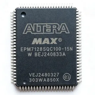
EPM7128SQI100-10N - 128-Macrocell MAX 7000S CPLD, 10ns, PQFP-100 | Intel / Altera
MPN: EPM7128SQI100-10N ✗ End of Life| Qty | Unit Price | Extended |
|---|---|---|
| 1 | $24.5 | $24.50 |
| 10 | $22.1 | $221.00 |
| 100 | $18.75 | $1,875.00 |
| 250 | $17.2 | $4,300.00 |
| 500 | $15.9 | $7,950.00 |
EPM7128SQI100-10N Overview
What is a CPLD? A Complex Programmable Logic Device is a non-volatile, reprogrammable digital IC that sits between simple PAL/GAL spld devices and high-density FPGAs. CPLDs (hierarchy: CPLD -> PLD -> programmable logic -> digital IC -> semiconductor) use a deterministic routing fabric and on-chip EEPROM/flash configuration memory, so they retain logic at power-up with no external boot PROM. The MAX 7000S family from Altera (now Intel FPGA) is a second-generation MAX architecture family widely used as glue logic, bus bridges, and state-machine controllers in industrial, telecom, and embedded designs.
Key features of the EPM7128SQI100-10N include 5-ns pin-to-pin delays (commercial speed grade), 100 MHz maximum operating frequency, IEEE Std. 1149.1 JTAG boundary-scan test (BST) circuitry, multiVolt I/O for 2.5 V / 3.3 V / 5 V interfacing, and individual macrocell clear/preset for synchronous or asynchronous control. The 'I' suffix indicates the industrial temperature grade (-40C to +85C), and the 'N' suffix indicates a lead-free / Pb-free RoHS-compliant assembly.
Architecturally, the EPM7128SQI100-10N organizes its 128 macrocells into four Logic Array Blocks (LABs) interconnected by a Programmable Interconnect Array (PIA). Each macrocell contains a programmable AND/OR array plus a configurable flip-flop with product-term clock, clear, and preset - giving designers 32 product terms per macrocell for sum-of-products logic. The deterministic PIA routing yields predictable, glitch-free timing that is independent of design placement - a key advantage over FPGAs for control-plane logic.
Typical applications include bus decoding and address mapping, peripheral chip-select generation, state-machine controllers, I/O expansion and bus bridging, glue logic between microprocessors and peripherals, and JTAG-controlled test access. The wide I/O count and PQFP-100 footprint make it well-suited for legacy industrial backplanes and 5 V-tolerant designs.
When designing with this device, ensure the VCCINT-to-VCCIO supply sequencing follows the datasheet monotonic-rise requirements and that unused I/O pins are correctly terminated (per AN 74). The JTAG chain should include the proper bypass instructions to avoid contention when multiple devices share TCK/TMS.
This page synthesizes distributor pricing, drop-in compatible alternatives, and practical design notes that go beyond the manufacturer datasheet to help engineers select, source, and apply the EPM7128SQI100-10N with confidence.
Drop-in alternatives for EPM7128SQI100-10N — same package, pin-to-pin compatible. Different-package parts requiring PCB rework are excluded.
Variants in this series
Same-series models that are drop-in compatible with EPM7128SQI100-10N (same form factor and footprint) — differing in Package, Usable Gates, Operating Temperature, Logic Array Blocks (LABs), Family.
Quick Comparison Tool — Select alternative parts for side-by-side comparison:
EPM7128SQI100-10
✅ Drop-In✓ In Stock
$9.75 / Unit
View Datasheet →EPM7128SQI100-7N
✅ Drop-In📋 Reference alternative (not in catalog)
EPM7128EQI100-15
✅ Drop-In✓ In Stock
$32.75 / Unit
View Datasheet →EPM7128AETI100-7N
✅ Drop-In✓ In Stock
$28.5 / Unit
View Datasheet →EPM7128SQC100-10
✅ Drop-In✓ In Stock
$9.85 / Unit
View Datasheet →EPM7128SQI100-10N Maximum Ratings & Electrical Characteristics
| Family | MAX 7000S |
| Device Type | CPLD - Complex Programmable Logic Device |
| Macrocells | 128 |
| Usable Gates | 2,500 (up to 5,000 usable in family) |
| Logic Array Blocks (LABs) | 4 |
| Maximum User I/Os | 84 |
| Pin-to-Pin Logic Delay (tPD) | 10 ns |
| Maximum Operating Frequency | 100 MHz |
| Counter Frequency (family max) | 175.4 MHz |
| Supply Voltage - Core (VCCINT) | 5.0 V |
| Supply Voltage - I/O (VCCIO) | 2.5 V / 3.3 V / 5.0 V (multiVolt) |
| Technology | CMOS, EEPROM-based configuration |
| Package | 100-pin PQFP (Plastic Quad Flat Pack) |
| Mounting Type | Surface Mount |
| Operating Temperature | -40C to +85C (Industrial grade, 'I' suffix) |
| Programming Interface | JTAG (IEEE Std. 1149.1) / ByteBlaster |
| RoHS Compliance | Compliant (lead-free, 'N' suffix) |
EPM7128SQI100-10N Pin Configuration
| Pin 1 | I/O — User I/O pin (macrocell 71) |
| Pin 2 | I/O — User I/O pin (macrocell 70) |
| Pin 3 | I/O — User I/O pin (macrocell 69) |
| Pin 4 | I/O — User I/O pin (macrocell 68) |
| Pin 5 | VCCINT — 5.0 V core supply |
| Pin 6 | I/O — User I/O pin (macrocell 67) |
| Pin 7 | I/O — User I/O pin (macrocell 66) |
| Pin 8 | I/O — User I/O pin (macrocell 65) |
| Pin 9 | I/O — User I/O pin (macrocell 64) |
| Pin 10 | GND — Ground |
| Pin 11 | I/O — User I/O pin (macrocell 63) |
| Pin 12 | I/O — User I/O pin (macrocell 62) |
| Pin 13 | I/O — User I/O pin (macrocell 61) |
| Pin 14 | I/O — User I/O pin (macrocell 60) |
| Pin 15 | I/O — User I/O pin (macrocell 59) |
| Pin 16 | I/O — User I/O pin (macrocell 58) |
| Pin 17 | I/O — User I/O pin (macrocell 57) |
| Pin 18 | I/O — User I/O pin (macrocell 56) |
| Pin 19 | VCCIO — I/O supply (2.5 / 3.3 / 5 V) |
| Pin 20 | I/O — User I/O pin (macrocell 55) |
| Pin 21 | I/O — User I/O pin (macrocell 54) |
| Pin 22 | I/O — User I/O pin (macrocell 53) |
| Pin 23 | I/O — User I/O pin (macrocell 52) |
| Pin 24 | GND — Ground |
| Pin 25 | I/O — User I/O pin (macrocell 51) |
| Pin 26 | I/O — User I/O pin (macrocell 50) |
| Pin 27 | I/O — User I/O pin (macrocell 49) |
| Pin 28 | I/O — User I/O pin (macrocell 48) |
| Pin 29 | I/O — User I/O pin (macrocell 47) |
| Pin 30 | I/O — User I/O pin (macrocell 46) |
| Pin 31 | I/O — User I/O pin (macrocell 45) |
| Pin 32 | I/O — User I/O pin (macrocell 44) |
| Pin 33 | I/O — User I/O pin (macrocell 43) |
| Pin 34 | VCCINT — 5.0 V core supply |
| Pin 35 | I/O — User I/O pin (macrocell 42) |
| Pin 36 | I/O — User I/O pin (macrocell 41) |
| Pin 37 | I/O — User I/O pin (macrocell 40) |
| Pin 38 | I/O — User I/O pin (macrocell 39) |
| Pin 39 | I/O — User I/O pin (macrocell 38) |
| Pin 40 | GND — Ground |
| Pin 41 | I/O — User I/O pin (macrocell 37) |
| Pin 42 | I/O — User I/O pin (macrocell 36) |
| Pin 43 | I/O — User I/O pin (macrocell 35) |
| Pin 44 | I/O — User I/O pin (macrocell 34) |
| Pin 45 | I/O — User I/O pin (macrocell 33) |
| Pin 46 | I/O — User I/O pin (macrocell 32) |
| Pin 47 | I/O — User I/O pin (macrocell 31) |
| Pin 48 | I/O — User I/O pin (macrocell 30) |
| Pin 49 | VCCIO — I/O supply (2.5 / 3.3 / 5 V) |
| Pin 50 | I/O — User I/O pin (macrocell 29) |
| Pin 51 | I/O — User I/O pin (macrocell 28) |
| Pin 52 | I/O — User I/O pin (macrocell 27) |
| Pin 53 | I/O — User I/O pin (macrocell 26) |
| Pin 54 | GND — Ground |
| Pin 55 | I/O — User I/O pin (macrocell 25) |
| Pin 56 | I/O — User I/O pin (macrocell 24) |
| Pin 57 | I/O — User I/O pin (macrocell 23) |
| Pin 58 | I/O — User I/O pin (macrocell 22) |
| Pin 59 | I/O — User I/O pin (macrocell 21) |
| Pin 60 | I/O — User I/O pin (macrocell 20) |
| Pin 61 | I/O — User I/O pin (macrocell 19) |
| Pin 62 | I/O — User I/O pin (macrocell 18) |
| Pin 63 | I/O — User I/O pin (macrocell 17) |
| Pin 64 | VCCINT — 5.0 V core supply |
| Pin 65 | I/O — User I/O pin (macrocell 16) |
| Pin 66 | I/O — User I/O pin (macrocell 15) |
| Pin 67 | I/O — User I/O pin (macrocell 14) |
| Pin 68 | I/O — User I/O pin (macrocell 13) |
| Pin 69 | I/O — User I/O pin (macrocell 12) |
| Pin 70 | GND — Ground |
| Pin 71 | TDI — JTAG Test Data In |
| Pin 72 | I/O — User I/O pin (macrocell 11) |
| Pin 73 | I/O — User I/O pin (macrocell 10) |
| Pin 74 | I/O — User I/O pin (macrocell 9) |
| Pin 75 | I/O — User I/O pin (macrocell 8) |
| Pin 76 | I/O — User I/O pin (macrocell 7) |
| Pin 77 | TMS — JTAG Test Mode Select |
| Pin 78 | TCK — JTAG Test Clock |
| Pin 79 | I/O — User I/O pin (macrocell 6) |
| Pin 80 | I/O — User I/O pin (macrocell 5) |
| Pin 81 | I/O — User I/O pin (macrocell 4) |
| Pin 82 | I/O — User I/O pin (macrocell 3) |
| Pin 83 | I/O — User I/O pin (macrocell 2) |
| Pin 84 | VCCIO — I/O supply (2.5 / 3.3 / 5 V) |
| Pin 85 | I/O — User I/O pin (macrocell 1) |
| Pin 86 | I/O — User I/O pin (macrocell 127) |
| Pin 87 | I/O — User I/O pin (macrocell 126) |
| Pin 88 | GND — Ground |
| Pin 89 | I/O — User I/O pin (macrocell 125) |
| Pin 90 | I/O — User I/O pin (macrocell 124) |
| Pin 91 | I/O — User I/O pin (macrocell 123) |
| Pin 92 | I/O — User I/O pin (macrocell 122) |
| Pin 93 | I/O — User I/O pin (macrocell 121) |
| Pin 94 | I/O — User I/O pin (macrocell 120) |
| Pin 95 | I/O — User I/O pin (macrocell 119) |
| Pin 96 | I/O — User I/O pin (macrocell 118) |
| Pin 97 | TDO — JTAG Test Data Out |
| Pin 98 | I/O — User I/O pin (macrocell 117) |
| Pin 99 | I/O — User I/O pin (macrocell 116) |
| Pin 100 | I/O — User I/O pin (macrocell 115) |
Typical Applications
EPM7128SQI100-10N is suitable for 6 applications: Microprocessor Bus Decode and Chip-Select Generation, Glue Logic and Peripheral I/O Expansion, State-Machine and Control-Plane Logic, Legacy Industrial Backplane and 5 V System Design, JTAG-Based Board Test and Boundary-Scan, Communication Protocol Bridging (UART / SPI / I2C / Parallel).
Microprocessor Bus Decode and Chip-Select Generation
The EPM7128SQI100-10N is ideal for microprocessor / microcontroller bus decoding thanks to its 128 macrocells and 84 user I/Os, which comfortably handle 24- to 32-bit address decoding plus multiple active-low chip-select outputs. Its 10 ns pin-to-pin delay keeps address-to-CS latency well below one 33 MHz bus cycle (30 ns), enabling clean zero-wait-state interfacing to MCUs, DSPs, and memory banks. The deterministic PIA routing of the MAX 7000S family yields predictable, placement-independent timing - critical for chip-select logic where any added glitch could mis-trigger a peripheral. Industrial temperature grade and 5 V tolerant I/O let the same CPLD serve across factory, telecom, and embedded backplane designs.
Recommended
Glue Logic and Peripheral I/O Expansion
When a microcontroller runs out of I/O pins or needs custom peripheral interfacing, the EPM7128SQI100-10N provides up to 84 user I/Os organized through four Logic Array Blocks, each with 16 macrocells. The CPLD's EEPROM-based configuration retains logic at power-up with no boot PROM required, simplifying board bring-up. With 10 ns tPD and 100 MHz fMAX, it can comfortably bridge slow peripherals to fast SPI, I2C, or UART busses, or generate PWM, quadrature decoding, and pulse-train outputs. The multiVolt I/O feature (2.5 V / 3.3 V / 5 V VCCIO) lets the same CPLD interface directly between modern low-voltage MCUs and legacy 5 V peripherals.
Recommended
State-Machine and Control-Plane Logic
The deterministic interconnect of the MAX 7000S architecture makes the EPM7128SQI100-10N an excellent platform for complex state machines, sequencers, and protocol controllers. Each macrocell offers up to 32 product terms plus a programmable flip-flop with separate clear, preset, and clock-enable signals - sufficient capacity for FSMs with 16 to 32 states. The 100 MHz fMAX accommodates USB full-speed, CAN 1 Mbps, and 10/100 Ethernet MAC-side interfaces. Industrial temperature grade and JTAG boundary-scan (BST) support production board-test access on telecom and industrial-control boards.
Recommended
Legacy Industrial Backplane and 5 V System Design
Many industrial backplanes, VME / cPCI cards, and factory-automation controllers are 5 V systems that require 5 V-tolerant CPLDs - a niche where the EPM7128SQI100-10N excels with its 5 V VCCINT and programmable VCCIO. The 100-pin PQFP package is widely supported on legacy backplane PCB layouts and can drive long bus traces through its 24 mA drive strength per pin. Industrial -40C to +85C operation and lead-free RoHS assembly make it compliant with current manufacturing standards while preserving the form, fit, and function of older designs.
Recommended
JTAG-Based Board Test and Boundary-Scan
The MAX 7000S family integrates IEEE Std. 1149.1 JTAG boundary-scan test (BST) circuitry on every I/O pin, making the EPM7128SQI100-10N a natural boundary-scan hub for production board-test architectures. With 84 I/Os, it can monitor interconnect continuity across large BGA devices on the same board and drive TEST_MODE signals across the test fixture. Quartus II programmer and USB-Blaster cable provide in-system programming through the same JTAG chain, eliminating socketed programming and enabling field firmware updates. Industrial temp grade and lead-free assembly suit telecom and automotive test-floor equipment.
Recommended
Communication Protocol Bridging (UART / SPI / I2C / Parallel)
The EPM7128SQI100-10N is frequently used as a bridge between mismatched communication interfaces - for example, converting a 16-bit parallel camera bus to SPI, or splitting a UART stream across multiple peripherals. Its 128 macrocells provide enough logic capacity to implement full-duplex UART with FIFO buffering, SPI master/slave with multi-CS, and I2C master state machines simultaneously. The 100 MHz fMAX and 10 ns tPD keep bit-rate latency low even at 10 Mbps SPI. The PQFP-100 footprint offers 84 user I/Os, enough to expose four independent serial channels and parallel control lines.
Recommended
Recommended Products Summary
Engineering reference data for EPM7128SQI100-10N — comparison, design guidance, and compliance information.
Selection Guide
Comparison with Alternatives
| Parameter | This Product | EPM7128SQI100-10 | EPM7128SQI100-7N | EPM7128EQI100-15 | EPM7128AETI100-7N | EPM7128SQC100-10 |
|---|---|---|---|---|---|---|
| Brand | Intel / Altera | Intel / Altera | Intel / Altera | Intel / Altera | Intel / Altera | Intel / Altera |
| Package | PQFP-100 | PQFP-100 - same | PQFP-100 - same | PQFP-100 - same | PQFP-100 - same | PQFP-100 - same |
| Macrocells | 128 | 128 | 128 | 128 | 128 | 128 |
| Pin-to-Pin Delay (tPD) | 10 ns | 10 ns | 7 ns (-30%, faster) | 15 ns (+50%, slower) | 7 ns (-30%, faster) | 10 ns |
| Temperature Grade | Industrial (-40C to +85C) | Industrial (-40C to +85C) | Industrial (-40C to +85C) | Industrial (-40C to +85C) | Industrial (-40C to +85C) | Commercial (0C to +70C) |
| RoHS / Lead-Free | Yes (N suffix) | No (leaded) | Yes (N suffix) | No (leaded) | Yes (N suffix) | No (leaded) |
| Usable Gates | 2,500 | 2,500 | 2,500 | 2,500 | 2,500 | 2,500 |
| User I/Os | 84 | 84 | 84 | 84 | 84 | 84 |
| Lifecycle Status | NRND | Obsolete / legacy stock | NRND | Obsolete / legacy stock | NRND | Obsolete / legacy stock |
Key Differentiators
- RoHS lead-free assembly with industrial temperature grade (vs EPM7128SQI100-10)
- 10 ns pin-to-pin delay balances cost and timing margin (vs EPM7128SQI100-7N)
- Industrial temperature support without redesign (vs EPM7128SQC100-10)
Design Notes
VCCINT must be a monotonic 5.0 V rise per the MAX 7000 datasheet Operating Requirements - any voltage dip during power-up can place the device into an undefined state and risk EEPROM configuration corruption. Use a supervisor IC (e.g., MAX811) or a well-bypassed 5 V LDO with at least 100 mA headroom. Place 0.1 uF ceramic decoupling on every VCCINT pin and a bulk 10 uF tantalum close to the PQFP-100 package. VCCIO can be tied to 2.5 V, 3.3 V, or 5 V independently; never leave it floating.
Route TCK and TMS away from high-frequency switching nets to avoid JTAG programming errors. Place the JTAG header within 50 mm of the CPLD pins to keep the TCK rise time clean and avoid signal-integrity issues on long stubs. Maintain at least 4 vias worth of thermal copper under the PQFP-100 thermal pad (exposed die-attach paddle) to keep junction temperature below 125 C at industrial ambient (Estimated: 1 W typical dissipation in MAX 7000S, theta_JA approximately 35 C/W in still air).
Do not assume any I/O pin can drive a 24 mA load without checking the VCCIO setting - high DC sink current at 5 V VCCIO with all outputs simultaneously asserted can exceed package power dissipation. Limit concurrent high-current outputs to 16-20 pins and derate for ambient > 50 C. Also, when migrating a programmed design from EPM7128SQI100-10 (leaded) to EPM7128SQI100-10N (lead-free), confirm the JTAG chain order and IDCODE match before field deployment - same die, but different device ID may report a different silicon revision.
Compliance Information
The 'N' suffix denotes lead-free matte-tin plating and RoHS compliance. Halogen-free status is not explicitly stated in the verified data and is marked unknown. AEC-Q100 is not applicable - this is a commercial / industrial CPLD, not an automotive-qualified part.