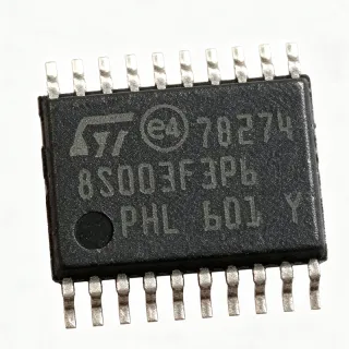
STM32G041F8P6 - 64MHz ARM Cortex-M0+ MCU | STMicroelectronics
MPN: STM32G041F8P6 ✓ Active| Qty | Unit Price | Extended |
|---|---|---|
| 1 | $1.85 | $1.85 |
| 10 | $1.67 | $16.70 |
| 100 | $1.48 | $148.00 |
| 500 | $1.33 | $665.00 |
| 1,000 | $1.2 | $1,200.00 |
Drop-in alternatives for STM32G041F8P6 — same package, pin-to-pin compatible. Different-package parts requiring PCB rework are excluded.
Quick Comparison Tool — Select alternative parts for side-by-side comparison:
STM32G031F8P6
✅ Drop-In📋 Reference alternative (not in catalog)
STM32G041F8P6TR
✅ Drop-In📋 Reference alternative (not in catalog)
STM32G041F8P6T
✅ Drop-In📋 Reference alternative (not in catalog)
LPC812M101JDH20
✅ Drop-In📋 Reference alternative (not in catalog)
EFM8BB21F16G-A-QFN20
✅ Drop-In📋 Reference alternative (not in catalog)
STM32G041F8P6 Maximum Ratings & Electrical Characteristics
| Core | ARM Cortex-M0+ |
| Maximum Clock Frequency | 64 MHz |
| Flash Memory | 32 KB |
| SRAM | 8 KB |
| Supply Voltage Range | 1.7 V to 3.6 V |
| Operating Temperature Range | -40°C to +85°C |
| Package | TSSOP-20 |
| ADC Resolution | 12-bit |
| ADC Channels | 19 |
| DAC Resolution | 12-bit |
| Timer Count | Multiple 16-bit timers |
| Communication Interfaces | I2C, SPI, USART |
| Low-Power RTC | Yes |
| Standby Current | 0.3 µA (typical) |
| Process Technology | 90nm |
| Internal Oscillator Accuracy | ±1% (calibrated HSI) |
| Hardware RNG | Yes |
| CRC Unit | Yes |
| Debug Interface | SWD |
| RoHS Status | Compliant |
STM32G041F8P6 Pin Configuration
| Pin 1 | VBAT — Battery backup supply for RTC |
| Pin 2 | PC14 — GPIO / OSC32_IN |
| Pin 3 | PC15 — GPIO / OSC32_OUT |
| Pin 4 | NRST — Reset (active low) |
| Pin 5 | VDD — Digital power supply |
| Pin 6 | VSS — Ground |
| Pin 7 | PA0 — GPIO / ADC_IN0 |
| Pin 8 | PA1 — GPIO / ADC_IN1 |
| Pin 9 | PA2 — GPIO / USART2_TX |
| Pin 10 | PA3 — GPIO / USART2_RX |
| Pin 11 | PA4 — GPIO / DAC_OUT1 |
| Pin 12 | PA5 — GPIO / SPI1_SCK |
| Pin 13 | PA6 — GPIO / SPI1_MISO |
| Pin 14 | PA7 — GPIO / SPI1_MOSI |
| Pin 15 | PB0 — GPIO / ADC_IN8 |
| Pin 16 | PB1 — GPIO / ADC_IN9 |
| Pin 17 | PB2 — GPIO / BOOT1 |
| Pin 18 | PB10 — GPIO / I2C2_SCL |
| Pin 19 | PB11 — GPIO / I2C2_SDA |
| Pin 20 | VDD — Digital power supply |
Safe Operating Area (SOA) & Thermal Characteristics
No official SOA curve available for this digital IC. Always operate within absolute maximum ratings specified in the datasheet. Ensure adequate cooling and derate as needed.
Typical Applications
STM32G041F8P6 is suitable for 6 applications: Industrial Sensors, Smart Home Devices, Portable Medical Monitors, Motor Control Systems, IoT Edge Nodes, Battery-Powered Devices.
Industrial Sensors
The STM32G041F8P6 is ideal for industrial sensor applications due to its 12-bit ADC with 19 channels, which can interface with various analog sensors. Its low power consumption and wide operating temperature range (-40°C to +85°C) ensure reliable operation in harsh industrial environments. The MCU's multiple communication interfaces (I2C, SPI, USART) allow easy integration with industrial networks. Its compact TSSOP-20 package enables space-saving designs in sensor modules. The 64 MHz Cortex-M0+ core provides sufficient processing power for sensor data acquisition and preprocessing. Additionally, the hardware CRC unit enhances data integrity in communication protocols.
Recommended
Smart Home Devices
The STM32G041F8P6 is well-suited for smart home devices such as smart thermostats, lighting controls, and security systems. Its ultra-low standby current of 0.3 µA extends battery life in wireless sensors and actuators. The integrated 12-bit ADC and DAC enable analog sensor interfacing and control signal generation. The MCU supports multiple low-power modes (Sleep, Stop, Standby) to optimize energy consumption. Its rich peripheral set, including timers and communication interfaces, allows seamless integration with Wi-Fi or Bluetooth modules. The compact TSSOP-20 package fits into small form-factor devices, making it ideal for modern smart home designs.
Recommended
Portable Medical Monitors
The STM32G041F8P6 is an excellent choice for portable medical monitors like pulse oximeters, glucose meters, and heart rate monitors. Its low power consumption (0.3 µA standby) is critical for battery-powered devices. The 12-bit ADC provides high-resolution measurement of biosignals, while the 12-bit DAC can generate analog outputs for alarms or calibration. The MCU's small TSSOP-20 package allows for miniaturized designs, essential for wearable medical devices. The hardware RNG enhances security for patient data encryption. The wide operating temperature range ensures reliable operation in various clinical environments.
Recommended
Motor Control Systems
The STM32G041F8P6 is suitable for motor control applications such as brushless DC (BLDC) motor drives and stepper motor controllers. Its multiple 16-bit timers can generate precise PWM signals for motor speed and direction control. The 12-bit ADC measures motor currents and voltages for closed-loop control. The 64 MHz clock speed provides fast processing for control algorithms like FOC (Field-Oriented Control). The MCU's low power consumption is beneficial for battery-powered motor applications. The compact package allows integration into motor driver modules. The hardware CRC unit ensures reliable communication in industrial motor control networks.
Recommended
IoT Edge Nodes
The STM32G041F8P6 is an ideal MCU for IoT edge nodes that collect data from sensors and transmit it to the cloud. Its low power consumption (0.3 µA standby) enables long battery life in remote sensors. The integrated ADC and communication interfaces (I2C, SPI, USART) allow easy connection to various sensors and wireless modules. The hardware RNG enhances security for secure communication protocols. The MCU's small TSSOP-20 package is perfect for compact IoT devices. The 64 MHz Cortex-M0+ core provides enough processing power for edge computing tasks like data filtering and aggregation.
Recommended
Battery-Powered Devices
The STM32G041F8P6 is specifically designed for battery-powered devices due to its ultra-low standby current of 0.3 µA and multiple low-power modes. It supports Sleep, Stop, and Standby modes, allowing designers to minimize power consumption during idle periods. The wide supply voltage range (1.7V to 3.6V) is compatible with single-cell batteries. The integrated peripherals reduce the need for external components, saving board space and power. The compact TSSOP-20 package is ideal for portable devices like remote controls, wearables, and wireless sensors. The 64 MHz clock speed ensures fast wake-up and processing when needed.
Recommended
Recommended Products Summary
Engineering reference data for STM32G041F8P6 — comparison, design guidance, and compliance information.
Selection Guide
Comparison with Alternatives
| Parameter | This Product | STM32G031F8P6 | LPC812M101JDH20 | EFM8BB21F16G-A-QFN20 |
|---|---|---|---|---|
| Package | TSSOP-20 | TSSOP-20 - same | TSSOP-20 - same | TSSOP-20 - same |
| Brand | STMicroelectronics | STMicroelectronics | NXP Semiconductors | Silicon Labs |
| Core | ARM Cortex-M0+ | ARM Cortex-M0+ | ARM Cortex-M0+ | 8051 |
| Max Clock Frequency | 64 MHz | 64 MHz | 30 MHz | 50 MHz |
| Flash Memory | 32 KB | 32 KB | 16 KB | 16 KB |
| SRAM | 8 KB | 8 KB | 4 KB | 2 KB |
| ADC Resolution | 12-bit | 12-bit | 12-bit | 12-bit |
| DAC | 12-bit | None | None | None |
| Standby Current | 0.3 µA | 0.3 µA | 1.5 µA | 0.5 µA |
| Hardware RNG | Yes | No | No | No |
Key Differentiators
- Integrated 12-bit DAC (vs STM32G031F8P6)
- Hardware Random Number Generator (RNG) (vs STM32G031F8P6)
- Lower standby current (vs LPC812M101JDH20)
Design Notes
Ensure proper decoupling of the VDD pins with 100nF capacitors placed as close to the pins as possible. Additionally, add a 4.7µF bulk capacitor on the main power rail. For battery-powered designs, utilize the low-power modes (Sleep, Stop, Standby) to minimize current consumption. The standby current is only 0.3 µA, but ensure all GPIOs are configured correctly to avoid leakage currents.
For the TSSOP-20 package, ensure the PCB footprint matches the recommended land pattern from the datasheet. Use a 0.65mm pitch with appropriate pad sizes. Place the crystal oscillator (if used) close to the OSC pins and keep traces short to minimize parasitic capacitance. For the SWD debug interface, route the SWDIO and SWCLK signals with controlled impedance if possible.
Do not exceed the absolute maximum ratings, especially the supply voltage of 3.6V. When using the internal HSI oscillator, calibrate it to achieve ±1% accuracy if precise timing is required. For applications using the ADC, ensure the reference voltage is stable and bypassed with a capacitor. Also, be aware that the STM32G041F8P6 does not have a dedicated VREF pin; the ADC reference is tied to VDD.
Compliance Information
RoHS compliant per STMicroelectronics product page. Not AEC-Q100 qualified - this is a standard grade MCU.