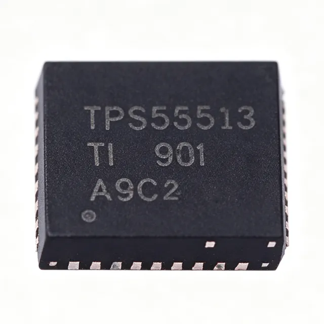
TPS53513RVER - 8A, 18V Sync Buck Converter | Texas Instruments
MPN: TPS53513RVER ✓ Active| Qty | Unit Price | Extended |
|---|---|---|
| 1 | $5.18 | $5.18 |
| 10 | $4.92 | $49.20 |
| 100 | $4.41 | $441.00 |
| 500 | $3.95 | $1,975.00 |
| 1,000 | $3.55 | $3,550.00 |
TPS53513RVER Overview
A synchronous buck converter is a type of DC-DC switching regulator that steps a higher input voltage down to a lower output voltage using two integrated MOSFETs (a high-side and a low-side switch) instead of an external Schottky diode. Within the power management IC hierarchy, it belongs to the family of switching voltage regulators, which achieve far higher efficiency than linear regulators, making them the standard choice for point-of-load power conversion in digital systems.
Key features of the TPS53513 include integrated 13.8-mOhm high-side and 5.9-mOhm low-side MOSFETs delivering 8 A of continuous output current, a precision 600 mV reference with 0.5% tolerance, support for all-ceramic output capacitors, and an integrated boost switch that eliminates one more external component.
Technically, the D-CAP3 control topology is an adaptive on-time architecture that provides fast transient response to load steps without complex loop compensation, allowing a very low external-component count. Because switching frequency adapts to input and output conditions, the converter maintains good efficiency across light and heavy loads while supporting high step-down ratios from 18 V rails.
Typical applications include powering FPGAs, ASICs, microprocessors, and DSP cores in networking, telecom, industrial, and server equipment, where a compact 8 A point-of-load solution from a 12 V intermediate bus is required.
For design, note the device is specified from -40C to +85C ambient; at 8 A loads with 18 V input, thermal design of the exposed-pad PCB land pattern is critical, and all-ceramic output capacitance must be verified against D-CAP3 stability requirements.
This page synthesizes distributor pricing, drop-in alternatives, comparison tables, and practical design notes not found in the manufacturer datasheet alone.
Drop-in alternatives for TPS53513RVER — same package, pin-to-pin compatible. Different-package parts requiring PCB rework are excluded.
Variants in this series
Same-series models that are drop-in compatible with TPS53513RVER (same form factor and footprint) — differing in Control Mode, Input Voltage Range, Package, Topology.
Quick Comparison Tool — Select alternative parts for side-by-side comparison:
TPS53515RVER
✓ In Stock
$3.18 / Unit
View Datasheet →TPS53513RVET
📋 Reference alternative (not in catalog)
TPS53513RVER Maximum Ratings & Electrical Characteristics
| Topology | Synchronous step-down (buck) converter |
| Control Mode | D-CAP3 adaptive on-time |
| Input Voltage Range | 1.5 V to 18 V |
| Output Voltage Range | 0.6 V to 5.5 V (adjustable) |
| Maximum Output Current | 8 A continuous |
| Reference Voltage | 600 mV +/-0.5% |
| High-Side MOSFET Rds(on) | 13.8 mOhm (integrated) |
| Low-Side MOSFET Rds(on) | 5.9 mOhm (integrated) |
| Number of Outputs | 1 |
| Output Capacitor Type | All-ceramic supported |
| Integrated Boost Switch | Yes |
| Operating Ambient Temperature | -40C to +85C |
| Package | 28-VFQFN Exposed Pad (RVE), VQFN-28 |
| Mounting Type | Surface Mount |
| Packing | Tape & Reel (R suffix) |
| RoHS Status | RoHS-Exempt & Green (per TI E2E forum) |
| Unit Price (reference) | $5.1761 (as of 2026-09-10, Heisener) |
TPS53513RVER 28-vfqfn exposed pad (rve), vqfn-28 Pin Configuration Guide
Pin configuration for TPS53513RVER (28-vfqfn exposed pad (rve), vqfn-28 package). This power device features gate, drain, and source terminals. For non-polarized packages, refer to the manufacturer datasheet for exact pin 1 orientation and footprint details. Common applications include power supply design, motor driving, and load switching.

No detailed pinout data available for TPS53513RVER.
Refer to the datasheet for full pin configuration.
Safe Operating Area
Typical Applications
TPS53513RVER is suitable for 6 applications: FPGA and ASIC Core Power, Networking and Telecom Equipment, Industrial Automation and Control, Server and Data Center Point-of-Load, DSP and Microprocessor Power, Compact Point-of-Load Modules.
FPGA and ASIC Core Power
The TPS53513RVER is well suited to powering FPGA and ASIC core rails because these loads combine high transient current steps with tight voltage windows. Its 8 A continuous rating covers mid-range FPGA core supplies, while the D-CAP3 adaptive on-time control responds to load steps within microseconds, minimizing droop on rails such as 1.0 V or 1.2 V derived from a 12 V intermediate bus. The 600 mV +/-0.5% reference supports low core voltages with margin to spare, and all-ceramic output capacitance keeps the solution height low for dense boards. Placed near the load with a compact inductor and ceramic output bank, the integrated 13.8-mOhm/5.9-mOhm MOSFET power stage delivers high efficiency without external FETs, though designers should budget board copper for thermal dissipation near full 8 A loads.
Recommended
Networking and Telecom Equipment
Networking switches, routers, and telecom line cards typically distribute a 12 V intermediate bus and need multiple compact point-of-load converters for MAC, PHY, and memory supplies. The TPS53513RVER fits this pattern directly: its 1.5 V to 18 V input accepts the 12 V bus with margin, and its 8 A capability covers high-draw digital loads such as switch ASICs and network processors. The very low external-component count of the D-CAP3 architecture shortens design time and reduces board area on dense line cards, while all-ceramic output capacitors improve long-term reliability expected in always-on telecom infrastructure. The -40C to +85C ambient specification covers telecom equipment environmental requirements, and the 28-VFQFN exposed pad package supports thermally enhanced layouts on standard multilayer PCBs.
Recommended
Industrial Automation and Control
Industrial control systems, PLCs, and motor-drive controllers demand robust, efficient point-of-load conversion from 12 V or 24 V-adjacent buses. The TPS53513RVER operates from 1.5 V to 18 V input, making it ideal for 12 V industrial rails, and its 8 A output powers embedded processors, DSPs, and I/O logic in one compact stage. The D-CAP3 control mode tolerates ceramic-only output networks, which resist vibration and dry-out failure modes that affect electrolytic capacitors in industrial environments. Its -40C to +85C ambient range matches unconditioned factory-floor enclosures. Because integrated MOSFETs remove external power-stage tuning, one proven design can be reused across product variants, reducing qualification effort. Careful exposed-pad soldering and copper pour are recommended to handle worst-case load and hot-ambient combinations.
Recommended
Server and Data Center Point-of-Load
Server motherboards and storage systems use distributed 12 V power architectures that feed many point-of-load converters for CPU auxiliaries, memory, ASICs, and SSD controllers. The TPS53513RVER serves mid-current rails up to 8 A with high efficiency from its integrated 13.8-mOhm and 5.9-mOhm MOSFETs, directly reducing converter losses and heat in thermally constrained chassis. The adaptive on-time D-CAP3 control handles the sharp load transients typical of bursty data-center workloads, and the 0.5%-accurate 600 mV reference enables low-voltage rails with tight regulation windows. All-ceramic output capacitance extends service life compared with electrolytic solutions, supporting the multi-year duty cycles expected of server hardware, while the small 28-VFQFN footprint preserves board space around dense processor power trees.
Recommended
DSP and Microprocessor Power
Digital signal processors and embedded microprocessors require stable low-voltage rails with good transient behavior during compute bursts. The TPS53513RVER delivers adjustable outputs from 0.6 V to 5.5 V, covering common 1.0 V, 1.2 V, 1.35 V, and 1.8 V DSP and MCU core and I/O supplies from a single 12 V or 5 V input. Its 8 A capacity suits higher-performance DSPs, while the fast D-CAP3 load-step response prevents core-voltage excursions during sudden processing loads that could trigger brownouts or clock throttling. The integrated boost switch simplifies the bootstrap design, reducing external-component count to an inductor, a few resistors, and ceramic capacitors. For lower-current DSP variants in the same family footprint, the 5 A TPS53515RVER offers a pin-compatible cost-optimized option.
Recommended
Compact Point-of-Load Modules
Power-module makers and board designers building small POL bricks benefit from the TPS53513RVER's very low external-component count: integrated MOSFETs, integrated boost switch, D-CAP3 control without external compensation, and all-ceramic output support mean the entire converter needs only an input filter, inductor, and small ceramic bank. The 28-VFQFN exposed pad package keeps the power stage compact, enabling high power density on standard PCBs. The wide 1.5 V to 18 V input range lets one module design serve 5 V, 12 V, and bus-derived inputs, simplifying product lines. The 8 A rating with a 0.5% 600 mV reference covers most digital rails. Thermal spreading through the exposed pad must be engineered into the module substrate, especially for continuous full-load operation in enclosed housings.
Recommended
Recommended Products Summary
Engineering reference data for TPS53513RVER — comparison, design guidance, and compliance information.
Selection Guide
Comparison with Alternatives
| Parameter | This Product | TPS53515RVER | TPS53513RVET |
|---|---|---|---|
| Package | 28-VFQFN Exposed Pad (RVE) | 28-VFQFN Exposed Pad (RVE) - same | 28-VFQFN Exposed Pad (RVE) - same |
| Brand | Texas Instruments | Texas Instruments | Texas Instruments |
| Maximum Output Current | 8 A | 5 A | 8 A |
| Input Voltage Range | 1.5 V to 18 V | 1.5 V to 18 V | 1.5 V to 18 V |
| Output Voltage Range | 0.6 V to 5.5 V | 0.6 V to 5.5 V | 0.6 V to 5.5 V |
| Control Mode | D-CAP3 adaptive on-time | D-CAP3 adaptive on-time | D-CAP3 adaptive on-time |
| Reference Voltage Tolerance | 600 mV +/-0.5% | 600 mV +/-0.5% | 600 mV +/-0.5% |
| RoHS / Green Status | RoHS-Exempt & Green | RoHS-Exempt & Green (per TI E2E) | RoHS-Exempt & Green (per TI E2E) |
Key Differentiators
- 8 A continuous current with fully integrated power stage (vs TPS53515RVER)
- D-CAP3 control with all-ceramic output support (vs TPS53626RSMR)
- Trade-off: fixed single-rail 8 A solution (vs TPS53515RVER)
Design Notes
The 28-VFQFN exposed pad is the primary thermal path for the TPS53513RVER; solder it to a solid ground plane with an array of thermal vias (typically 5x5 or larger under the pad). Estimated: at 8 A load and 12 V to 1.2 V conversion, high-side conduction loss alone is roughly I2 x Rds(on) x duty = 64 x 0.0138 x 0.1, about 0.09 W, but switching losses at high VIN and high frequency add significantly - verify junction temperature with the datasheet thermal metrics and your switching frequency. Keep hot ambient derating in mind: the device is specified to +85C ambient.
Place the input ceramic capacitors, inductor, and output capacitors as close to the IC as possible. Keep the SW node (inductor connection) copper area small to reduce radiated EMI, and route the feedback trace away from the switch node and inductor to avoid noise coupling into the 600 mV reference node. Use a solid ground plane under the converter and connect the exposed pad directly to it with multiple vias. Follow the PCB layout guidelines in the TI TPS53513 datasheet, which provides a proven two-layer and four-layer layout example.
Although the TPS53513 supports all-ceramic output capacitors, verify total output capacitance against the D-CAP3 stability and transient requirements in the datasheet - excessive ceramic capacitance can affect adaptive on-time behavior during startup. Do not exceed the 18 V absolute maximum on VIN; add margin or a TVS on supply rails with transients. Set the output voltage with 1%-tolerance resistors to preserve the 0.5% reference accuracy. Note the R and T orderable suffixes are the same silicon (TI E2E confirmation) - buy whichever reel quantity is available.
Compliance Information
Per TI E2E forum response, TPS53513RVER and TPS53513RVET are RoHS-Exempt & Green. Green indicates halogen-free packaging. REACH, lead-free, and conflict-minerals status should be confirmed on the TI.com quality/environmental pages.






