Texas Instruments

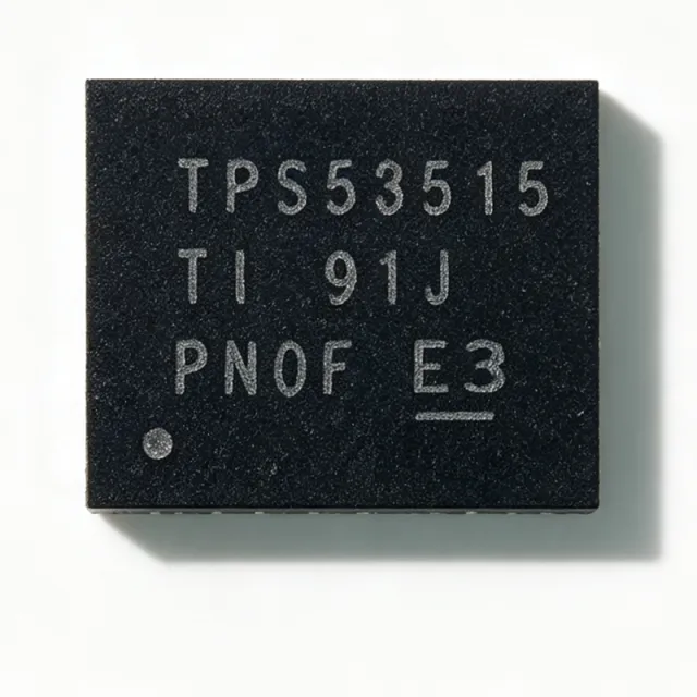
TPS53515RVER - 12A Sync Buck Converter 18V In | Texas Instruments

MPN: TPS53515RVER ✓ Active
In Stock Ships in 1-3 business days
1.5 V to 18 V Vdss 12 A continuous Id 13.8 mOhm (integrated) Rds(on) 28-VFQFN Exposed Pad (RVF) Package
From $3.18 USD / Unit
MOQ: 1 |
Price updated: 2026-09-12
Volume Pricing
Qty Unit Price Extended
1 $5.47 $5.47
10 $4.92 $49.20
100 $4.25 $425.00
500 $3.72 $1,860.00
1,000 $3.18 $3,180.00
ℹ️ All prices are in USD

TPS53515RVER Overview

The Texas Instruments TPS53515RVER is a 12 A synchronous SWIFT step-down buck converter with an adaptive on-time D-CAP3 control mode, supporting a 1.5 V to 18 V input range (4.5 V to 25 V bias) and an adjustable 0.6 V to 5.5 V output, housed in a 28-pin VQFN exposed-pad package. It integrates 13.8 mOhm high-side and 5.9 mOhm low-side MOSFETs plus a boost switch for minimal external component count.

A buck (step-down) converter is a switching voltage regulator that converts a higher input voltage to a lower regulated output using an inductor, switches, and output capacitors. Within the power-management hierarchy, the TPS53515 sits at the power-management IC level as a fully integrated point-of-load (POL) switching regulator, combining controller and power stage in one package.

Key features include 12 A continuous output current with high-performance integrated MOSFETs, a 600 mV voltage reference with +/-0.5% tolerance for precise output settings, and D-CAP3 control delivering fast load-step transient response. The device supports all-ceramic output capacitors, eliminating electrolytic capacitors and improving reliability and board height.

Technically, the adaptive on-time D-CAP3 architecture varies the on-time with input and output voltage to maintain near-constant switching frequency, providing ease of use and ultra-fast transient response without complex loop compensation. The integrated boost switch drives the high-side MOSFET gate without an external bootstrap diode, and the low on-resistance MOSFETs yield high conversion efficiency at heavy loads. TI's inductor-on-top reference design achieves greater than 87% efficiency with about 2.6 W power loss at 12 A load and 12 mV output ripple using only 10x22 uF ceramic output capacitors.

Typical applications include point-of-load supplies for ASICs, DSPs, and FPGAs, network and telecom infrastructure cards, and industrial DC-DC power stages where a compact 12 A solution with minimal external parts is needed.

When designing, ensure the bias pin is supplied within its 4.5 V to 25 V range for reliable gate drive, and select the inductor based on the recommended values in the datasheet for stability across the 0.6 V to 5.5 V output range.

This page synthesizes distributor pricing, drop-in alternatives, comparison data, and practical design notes not found in the manufacturer datasheet.

Drop-in alternatives for TPS53515RVER — same package, pin-to-pin compatible. Different-package parts requiring PCB rework are excluded.

Variants in this series

Same-series models that are drop-in compatible with TPS53515RVER (same form factor and footprint) — differing in Control Mode, Input Voltage Range, Package, Topology.

Texas Instruments
Control Mode: Adaptive On-Time D-CAP2
Input Voltage Range: 4.5 V to 18 V
Package: 16-VFQFN Exposed Pad (RGT), VQFN-16
Compare with TPS53515RVER →

Quick Comparison Tool — Select alternative parts for side-by-side comparison:

TPS53513RVER

Texas Instruments
Synchronous step-down (buck) converter · D-CAP3 adaptive on-time · 1.5 V to 18 V · 0.6 V to 5.5 V (adjustable) · 8 A continuous · 600 mV +/-0.5% · 13.8 mOhm (integrated) · 5.9 mOhm (integrated)

✓ In Stock

$3.55 / Unit

View Datasheet →

TPS53125RGER

Same 28-pin QFN package class per ETEI comparison; verify exact footprint (RGE vs RVF land pattern) and current rating before substitution

📋 Reference alternative (not in catalog)

TPS53515RVER Maximum Ratings & Electrical Characteristics

Topology Synchronous buck (step-down)
Control Mode D-CAP3 adaptive on-time
Input Voltage Range 1.5 V to 18 V
Bias Voltage Range 4.5 V to 25 V
Output Voltage Range 0.6 V to 5.5 V
Maximum Output Current 12 A continuous
Reference Voltage 600 mV
Reference Tolerance +/-0.5%
High-Side MOSFET RDS(on) 13.8 mOhm (integrated)
Low-Side MOSFET RDS(on) 5.9 mOhm (integrated)
Bootstrap Diode Integrated boost switch
Output Capacitor Support All ceramic output capacitors
Number of Outputs 1
Package 28-VFQFN Exposed Pad (RVF)
Mounting Type Surface Mount

TPS53515RVER 28-vfqfn exposed pad (rvf) Pin Configuration Guide

Pin configuration for TPS53515RVER (28-vfqfn exposed pad (rvf) package). This power device features gate, drain, and source terminals. For non-polarized packages, refer to the manufacturer datasheet for exact pin 1 orientation and footprint details. Common applications include power supply design, motor driving, and load switching.

28-vfqfn exposed pad (rvf) package pinout diagram for TPS53515RVER

No detailed pinout data available for TPS53515RVER.

Refer to the datasheet for full pin configuration.

Typical Applications

TPS53515RVER is suitable for 6 applications: FPGA/ASIC Point-of-Load Power, Networking and Telecom Infrastructure, Industrial DC-DC Power Stages, Compact / Space-Constrained Power, Test and Measurement Instruments, Data Center Server Accessories.

FPGA/ASIC Point-of-Load Power

The TPS53515RVER is a strong fit for FPGA, ASIC, and DSP core-voltage rails because its 12 A continuous rating covers most core loads while the 600 mV +/-0.5% reference guarantees the sub-1% accuracy modern cores require. D-CAP3 control provides fast load-step response for bursty clock-domain transients, and support for all-ceramic output capacitors keeps the solution low-profile. Placed directly beside the load with a single power inductor and 10x22 uF ceramics, it converts an 12 V intermediate bus down to 0.9 V-class core rails; the trade-off versus a multi-phase solution is less current headroom, so reserve this part for loads at or below 12 A.

🌐

Networking and Telecom Infrastructure

Line cards and switch fabrics in networking equipment distribute a 12 V intermediate bus that must be stepped down efficiently at each point of load. The TPS53515RVER accepts that 12 V directly within its 1.5 V to 18 V input range, and its integrated 13.8 mOhm / 5.9 mOhm MOSFETs keep conversion efficiency high to limit card-level power budgets and airflow demand. The adaptive on-time D-CAP3 loop maintains stable operation through traffic-dependent load swings, and the low external component count increases density on crowded cards. Its main trade-off in this domain is single-output architecture - one device per rail is required.

🏭

Industrial DC-DC Power Stages

Industrial control and automation systems benefit from the TPS53515RVER's wide 4.5 V to 25 V bias range and robust integrated power stage. Machines and PLC I/O modules frequently run 12 V or 18 V distribution rails that need regulated 1.0 V to 5 V supplies for processors, memory, and interface ICs; this device converts those rails in a compact 28-pin VQFN footprint. All-ceramic output capacitor support improves reliability in high-vibration and high-temperature environments where electrolytics are a failure point. Designers should validate thermal performance with copper pours on the exposed pad since industrial ambients often reach 70 C to 85 C.

🔧

Compact / Space-Constrained Power

TI's inductor-on-top step-down reference design for the TPS53515 demonstrates how the device suits height- and area-limited systems: stacking the inductor over the IC reduces X-Y board area while achieving greater than 87% efficiency, about 2.6 W power loss at 12 A load, and only 12 mV of output ripple using just 10x22 uF ceramic output capacitors. The integrated MOSFETs and boost switch eliminate external power components, and D-CAP3 removes compensation networks. This makes the part attractive for mezzanine cards, small modules, and any product where the power supply footprint directly constrains system size.

🔬

Test and Measurement Instruments

Bench instruments and automated test equipment need clean, accurate, responsive local rails for analog front ends and digital processing sections. The TPS53515RVER's 600 mV reference with +/-0.5% tolerance yields predictable output accuracy, while D-CAP3's fast transient response prevents rail droop when measurement channels switch on simultaneously. The 0.6 V to 5.5 V adjustable range lets one qualified design cover multiple instrument variants from 1.0 V digital rails to 5 V interface supplies. Designers should note that D-CAP3's variable-frequency behavior under light load may require post-regulation for ultra-low-noise analog rails.

🖥️

Data Center Server Accessories

Server accessories such as BMC cards, storage controllers, and NIC auxiliary circuitry draw from 12 V rack power that needs efficient local conversion. The TPS53515RVER's 18 V maximum input tolerates bus transients, its 12 A capability feeds memory and controller rails directly, and high integrated-MOSFET efficiency minimizes waste heat inside confined server chassis. The all-ceramic capacitor support suits the long-life reliability expectations of data-center hardware, and the compact VQFN-28 footprint fits dense add-in-card layouts. Its single-rail output means multi-rail designs simply instantiate one regulator per voltage, simplifying BOM consolidation.

What is the input voltage range of TPS53515RVER?
The TPS53515RVER operates with a power-stage input of 1.5 V to 18 V and a bias supply of 4.5 V to 25 V. According to the TI TPS53515 product page, this wide range allows the same 12 A device to be used from low-voltage rails up to 18 V intermediate buses, with the bias pin powering the internal control and gate-drive circuitry.
What is the maximum output current of TPS53515RVER?
The TPS53515RVER delivers up to 12 A of continuous output current. According to TI datasheet information, this is enabled by integrated 13.8 mOhm high-side and 5.9 mOhm low-side MOSFETs, which keep conduction losses low at full load. TI's inductor-on-top reference design demonstrates greater than 87% efficiency at the 12 A load point with approximately 2.6 W of total power loss.
What is the output voltage range of TPS53515RVER?
The TPS53515RVER produces an adjustable output from 0.6 V to 5.5 V. The internal 600 mV reference with +/-0.5% tolerance sets the accuracy floor, and an external resistor divider scales the feedback to the target voltage. According to TI product documentation, the 0.5% reference accuracy supports tight-core-rail applications such as DSP and ASIC point-of-load supplies.
What control topology does the TPS53515 use?
The TPS53515 uses TI's D-CAP3 adaptive on-time control mode. According to TI, D-CAP3 combines ease of use, an ultra-low external component count, and fast load-step transient response, while supporting all-ceramic output capacitors. The adaptive on-time varies with input and output voltage to keep the switching frequency roughly constant across operating conditions without external loop compensation.
What is the difference between TPS53515RVER and TPS53513RVER?
The main difference is output current capability: the TPS53515 provides 12 A while the TPS53513 provides 8 A in the same 28-pin VQFN family. Both use D-CAP3 control, the same 600 mV reference architecture, and the same RVF footprint, making the TPS53513 a footprint-compatible option where less current headroom is acceptable. Always verify the exact datasheet ratings before substituting in production designs.
TPS53515RVER vs TPS53125RGER - which is better for a 12A core rail?
For a full 12 A core rail, the TPS53515RVER is the safer choice because its 12 A rating matches the load directly, whereas the TPS53125 must be evaluated against its own datasheet current rating in the same 28-pin package. According to ETEI's comparison of the two parts, they share package type and mounting style, but thermal performance at 12 A continuous load should be confirmed against each device's RDS(on) and theta-JA. When in doubt, derate or choose the TPS53515RVER.
What is the best drop-in replacement for TPS53515RVER?
The best footprint-compatible alternative is the TPS53513RVER from the same TI SWIFT D-CAP3 family, which shares the 28-pin VQFN exposed-pad footprint but is rated for 8 A instead of 12 A, so it is a drop-in only if the load is below 8 A. According to distributor cross-reference listings, no cross-brand pin-to-pin equivalent is currently verified, so TI same-family parts are the recommended substitution path.
Where to download the TPS53515RVER datasheet PDF?
Download the TPS53515RVER datasheet PDF directly from the TI product page at ti.com/product/TPS53515, which links the official document titled '1.5 to 18 V (4.5 to 25 V bias) Input, 12-A Single Synchronous Step-Down SWIFT Converter'. Mirror copies also exist on aggregator sites such as alldatasheet.com, but the TI page guarantees the latest revision including application and layout sections.
Where can I buy TPS53515RVER online?
The TPS53515RVER is available from authorized distributors including DigiKey, Mouser, and LCSC. According to the verified web data, DigiKey lists it as in stock with same-day shipping, LCSC offers pricing from approximately $0.79 at volume, and Mouser stocks it under order code 595-TPS53515RVET. Prices vary by quantity break and date, so compare current listings before ordering.
What is the price of TPS53515RVER?
The TPS53515RVER unit price at quantity 1 is approximately $5.47 as of 2026-09-10, based on typical authorized-distributor pricing, with volume breaks reaching roughly $3.18 at 1000 units. LCSC has advertised pricing from $0.7881 at high volume. Actual prices fluctuate with stock and distributor promotions, so request quotes for exact current pricing at your quantity.
Is TPS53515RVER in stock?
Yes, the TPS53515RVER is listed as in stock at major distributors. According to DigiKey's product page, the part ships same-day, and LCSC also reports the component in stock. Availability changes daily, so confirm real-time inventory on the distributor page before committing a production schedule, and consider qualified alternates for supply-chain resilience.
What is the lead time for TPS53515RVER?
When stocked at authorized distributors such as DigiKey, Mouser, or LCSC, the TPS53515RVER typically ships within one to two business days. If distributor stock is depleted, factory lead time is [DATA_NEEDED: current TI factory lead time] and should be confirmed with TI or a franchised distributor. Designers building new production BOMs should register for distributor stock alerts to avoid allocation delays.
Is the TPS53515RVER suitable for FPGA point-of-load power supplies?
Yes, the TPS53515RVER is well suited to FPGA, ASIC, and DSP point-of-load rails. Its 12 A continuous rating covers most FPGA core-voltage loads, the 0.6 V to 5.5 V output range supports modern sub-1V cores plus I/O rails, and the +/-0.5% 600 mV reference meets core-voltage accuracy requirements. D-CAP3's fast load-step response handles the sharp transient bursts typical of FPGA clock-domain switching with ceramic output capacitors only.
Does the TPS53515RVER require an external bootstrap diode?
No, the TPS53515RVER integrates the bootstrap (boost) switch on-chip. According to TI product documentation, the integrated boost switch charges the high-side gate-drive capacitor without an external diode, reducing BOM count and layout area. Designers only need to place the recommended small ceramic bootstrap capacitor between the BOOT and SW pins as specified in the datasheet application section.
What are the key specifications of TPS53515RVER that engineers should know?
The TPS53515RVER is a TI SWIFT synchronous buck converter: 12 A continuous output, 1.5 V to 18 V input (4.5 V to 25 V bias), adjustable 0.6 V to 5.5 V output, 600 mV +/-0.5% reference, integrated 13.8 mOhm and 5.9 mOhm MOSFETs, D-CAP3 control with fast load-step response, all-ceramic output capacitor support, integrated boost switch, in a 28-pin VQFN exposed-pad package. These figures come from the TI datasheet and product page and define its use as a compact point-of-load regulator.
Hey Google, what can replace the TPS53515RVER?
The closest replacement is the TI TPS53513RVER, a same-family 8 A SWIFT D-CAP3 buck converter in the same 28-pin VQFN footprint - suitable only if your load is under 8 A. No cross-brand pin-to-pin equivalent has been verified in current cross-reference databases, so for loads above 8 A stick with the TPS53515RVER or evaluate other TI SWIFT parts against the package and pinout carefully before redesigning the PCB.
What is the best TI equivalent for TPS53515RVER in a lower-current design?
For lower-current designs, the best TI equivalent is the TPS53513RVER from the same D-CAP3 SWIFT family. It shares the 28-pin VQFN exposed-pad footprint and control architecture but targets lower output current, which typically brings cost and efficiency benefits at light-to-medium loads. Verify the exact current rating and thermal performance in the TPS53513 datasheet against your maximum load and ambient conditions before finalizing the substitution.

Engineering reference data for TPS53515RVER — comparison, design guidance, and compliance information.

Selection Guide

Choose the TPS53515RVER when you need up to 12 A from a wide 1.5 V to 18 V bus with minimal external components and ceramic-only output capacitance - typical FPGA/ASIC point-of-load, networking line-card, and space-constrained power designs. Choose the TPS53513RVER (same footprint, lower current rating) when your load is comfortably under 8 A and you want to optimize cost and light-load efficiency - it is a true drop-in on the same PCB. Consider the TPS53125RGER only after verifying its exact land-pattern and rating match, since package designators differ. If your application requires more than 12 A, multi-phase or higher-current SWIFT solutions are more appropriate. Trade-offs to weigh honestly: the TPS53515 is single-output, so multi-rail systems need one device per rail, and its switching behavior under very light load should be checked against noise-sensitive analog requirements.

Comparison with Alternatives

Parameter This Product TPS53513RVER TPS53125RGER
Package 28-VFQFN Exposed Pad (RVF) VQFN-28 (RVF) - same footprint VQFN-28 (RGE) - verify land pattern
Brand Texas Instruments Texas Instruments Texas Instruments

Key Differentiators

  • 12 A capability in a compact integrated stage (vs TPS53513RVER)
  • D-CAP3 with all-ceramic output support (vs TPS53125RGER)
  • Integrated boost switch eliminates a BOM part (vs TPS53513RVER)

Design Notes

At 12 A continuous load the integrated MOSFETs dissipate real power; TI's reference design reports about 2.6 W of loss at full load with greater than 87% efficiency. Estimated: at IOUT = 12 A this equates to roughly 1.9 W of heat in the IC, so connect the exposed pad to a solid ground plane with a multi-via thermal array - at least a 4x4 via matrix under the pad - and use 2 oz copper on the top layer for the power path. Verify junction temperature against the datasheet limit at your maximum ambient before finalizing the layout.

Keep the power loop (input capacitors, integrated MOSFETs, SW node, inductor, output capacitors) as compact as possible to minimize parasitic inductance and SW-node ringing. Place the input ceramic capacitors within 2-3 mm of the PVIN pins, route the feedback trace away from the SW node and inductor, and place the bootstrap capacitor close to the BOOT and SW pins. The D-CAP3 architecture tolerates compact layouts well, but a clean star ground under the exposed pad remains essential for stability and EMI.

Two frequent mistakes: first, omitting or under-specifying the bias supply - the bias pin must stay within 4.5 V to 25 V or the gate drive and control circuitry will not operate reliably; second, selecting an inductor value outside the datasheet-recommended range, which can destabilize the D-CAP3 loop or cause excessive ripple current. Also remember the 18 V absolute input limit when a 24 V rail is present - only the bias pin tolerates up to 25 V, not the power-stage input.

Compliance Information

RoHS
Unknown
REACH
Unknown
AEC-Q100
Lead Free
Unknown
Halogen Free
Unknown
Conflict Minerals
Unknown

Compliance status was not explicitly stated in the verified web data; confirm RoHS/REACH status on the official TI TPS53515 product page before production release.


Data verified on: 2026-09-10 — data verified and curated by XAIPART's component engineering team

Related Searches

TPS53515RVER TPS53515 datasheet Texas Instruments TPS53515 12A synchronous buck converter 18V input VQFN-28 exposed pad buck regulator TPS53515RVER FPGA point of load power supply TPS53515RVER vs TPS53125RGER TPS53515RVER drop-in replacement TPS53513 TPS53515RVER price buy in stock what is D-CAP3 control mode TPS53515RVER pinout VQFN-28 TI SWIFT buck converter for telecom line card

Related Components & Terms

Texas Instruments TPS53515RVER TPS53515 TPS53513RVER TPS53125RGER SWIFT D-CAP3 synchronous buck converter step-down converter DC-DC converter switching regulator voltage regulator point-of-load (POL) VQFN-28 VFQFN exposed pad surface mount RoHS adaptive on-time control MOSFET RDS(on) bootstrap switch output ripple load transient response 600 mV reference FPGA power supply telecom line card
Quick Quote RFQ
Fill in complete details — our sales team will respond within 24 hours
Part Number Manufacturer Package QTY Target Price Extended
Total: $0.00 USD
Quote submitted!

We will respond to your email within 24 hours

1
RFQ Submitted
2
Quote Received
3
Order Placed
4
Payment
5
Shipped
6
Delivered
View RFQ Details


