Texas Instruments

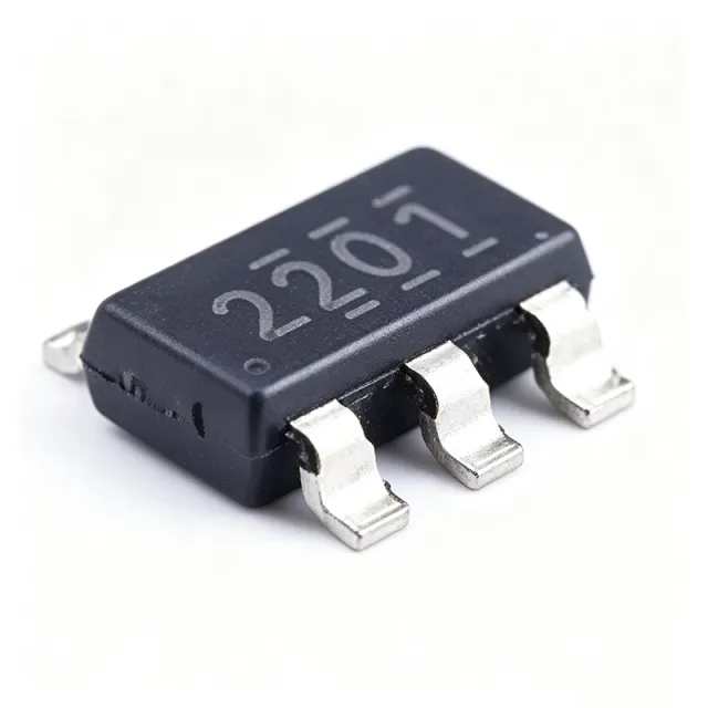
TPS562201DDCT - 2A 17V Sync Buck Converter | Texas Instruments

MPN: TPS562201DDCT βœ“ Active
In Stock Ships in 1-3 business days
4.5 V to 17 V Vdss 2 A Id SOT-23-Thin (TSOT-23-6, DDC), 2.9 mm x 1.6 mm Package 580 kHz (fixed) Speed
From $0.45 USD / Unit
MOQ: 1 |
Price updated: 2026-09-01
Volume Pricing
Qty Unit Price Extended
1 $0.68 $0.68
10 $0.61 $6.10
100 $0.55 $55.00
500 $0.49 $245.00
1,000 $0.45 $450.00
ℹ️ All prices are in USD

Drop-in alternatives for TPS562201DDCT β€” same package, pin-to-pin compatible. Different-package parts requiring PCB rework are excluded.

Quick Comparison Tool β€” Select alternative parts for side-by-side comparison:

TPS562208DDCR

βœ… Drop-In
πŸ“¦ SOT-23-6 (DDC)
same 2A rating and SOT-23-6 footprint; FB reference 0.6V vs 0.768V (-22%) enabling outputs below 0.768V - FB divider must be recalculated

πŸ“‹ Reference alternative (not in catalog)

TPS562200DDCR

βœ… Drop-In
πŸ“¦ SOT-23-6 (DDC)
same D-CAP2 family, same SOT-23-6 footprint; rated 1.5A vs 2A output current (-25%) per distributor cross-reference data

πŸ“‹ Reference alternative (not in catalog)

TPS563207DRLR

βœ… Drop-In ⚠️ 参数待ιͺŒθ―
Texas Instruments
πŸ“¦ SOT-23-6 (DDC)
Synchronous Buck (Step-Down) Β· 4.3 V to 17 V Β· 0.806 V adjustable Β· 3 A Β· D-CAP2 mode Β· Forced CCM (FCCM) Β· 1 Β· Positive, Adjustable

βœ“ In Stock

$0.31 / Unit

View Datasheet β†’

TPS563201DDCR

βœ… Drop-In ⚠️ 参数待ιͺŒθ―
πŸ“¦ SOT-23-6 (DDC)
3A output vs 2A (+50% headroom), same D-CAP2 control and SOT-23-6 (DDC) package; verifies pin-compatible family operation at higher current

πŸ“‹ Reference alternative (not in catalog)

TPS561201DDCR

βœ… Drop-In ⚠️ 参数待ιͺŒθ―
Texas Instruments
πŸ“¦ SOT-23-6 (DDC)
Synchronous Step-Down (Buck) Β· 4.5 V to 17 V Β· 0.76 V to 7 V (adjustable) Β· 1 A Β· 580 kHz (fixed) Β· D-CAP2 Β· 0.4 mA (typ) Β· -40C to +125C

βœ“ In Stock

$0.29 / Unit

View Datasheet β†’

TPS562201DDCT Maximum Ratings & Electrical Characteristics

Topology Synchronous step-down (buck)
Input Voltage Range 4.5 V to 17 V
Output Voltage Range 0.768 V to 7 V (adjustable)
Maximum Output Current 2 A
Switching Frequency 580 kHz (fixed)
Control Scheme D-CAP2 (adaptive on-time, internally compensated)
Light Load Mode Eco-mode pulse-skip
Integrated MOSFETs High-side and low-side FETs (synchronous)
Number of Outputs 1
Operating Temperature -40C to +125C (junction)
Package SOT-23-Thin (TSOT-23-6, DDC), 2.9 mm x 1.6 mm
Mounting Type Surface Mount
Feedback Voltage 0.768 V
Protection Features Internal soft-start, overcurrent protection
RoHS Status Compliant
Packaging Cut Tape (DDCT) / Tape & Reel (DDCR)

TPS562201DDCT Pin Configuration

SOT-23 Package Pinout Diagram SOT-23 3-pin surface mount transistor, JEDEC TO-236. Pin 1 by dot. 1 2 3 SOT-23
Pin 1 BOOT β€” Bootstrap capacitor connection for high-side gate driver
Pin 2 GND β€” Ground reference
Pin 3 SW β€” Switch node - connect to output inductor
Pin 4 VIN β€” Input supply, 4.5 V to 17 V
Pin 5 FB β€” Feedback input - resistor divider from VOUT
Pin 6 EN β€” Enable pin (do not float; tie high or low)

Safe Operating Area (SOA) & Thermal Characteristics

Safe Operating Area Chart Default safe operating area chart for TPS562201DDCT Drain-to-Source Voltage (Vds) Drain Current (Id)

No official SOA curve available for this component. Always operate within absolute maximum ratings specified in the datasheet. Ensure adequate cooling and derate as needed.

Typical Applications

TPS562201DDCT is suitable for 6 applications: 12V Distributed Power Point-of-Load, Networking and Telecom Equipment, Industrial Automation Systems, Set-Top Boxes and Digital TV, SSD and Storage Peripheral Power, IoT and Smart Home Hubs.

⚑

12V Distributed Power Point-of-Load

The TPS562201DDCT is a natural fit for point-of-load regulation on 12V distributed power buses. Its 4.5V to 17V input range directly accepts 12V rails with margin for bus tolerance, and the 0.768V to 7V adjustable output covers 1.0V, 1.2V, 1.8V, 2.5V, 3.3V, and 5V logic rails. The D-CAP2 control loop provides fast transient response for dynamic processor loads, while the 580 kHz frequency keeps the inductor small. In a typical 12V-to-3.3V, 2A configuration, the synchronous topology maintains high efficiency without an external Schottky diode, and the 2.9 mm x 1.6 mm SOT-23-Thin package fits directly under dense BGA footprints.

🌐

Networking and Telecom Equipment

Switches, routers, and telecom line cards commonly run from 12V backplane feeds and need multiple efficient local rails. The TPS562201DDCT's 17V maximum input covers these buses directly, and Eco-mode pulse-skip operation keeps standby efficiency high when ports are idle - important for energy-efficient Ethernet and green-datacenter requirements. The D-CAP2 architecture handles the fast load steps that occur when port PHYs power up, and the internally compensated loop eliminates external compensation components, reducing BOM count on high-density line cards. Its 580 kHz fixed frequency also keeps switching noise out of sensitive baseband bands, and the -40C to +125C junction range suits unventilated telecom enclosures.

🏭

Industrial Automation Systems

Industrial controllers, sensors, and I/O modules require robust, wide-input, small-footprint power conversion. The TPS562201DDCT tolerates the supply variation typical of 24V-derived 12V auxiliary buses, and internal soft-start plus overcurrent protection simplify qualification for factory environments. The D-CAP2 loop's fast transient response supports FPGA and MCU loads that step between sleep and active modes, while Eco-mode keeps light-load draw low in always-on monitoring nodes. The 1.6 mm x 2.9 mm package and minimal external component count enable compact designs on standard industrial PCBs, and the -40C cold-start rating matches unheated cabinet installations common in factory automation deployments.

πŸ“Ί

Set-Top Boxes and Digital TV

Set-top box and digital TV power architectures historically standardized on the D-CAP2 SOT-23 converter family, and the TPS562201DDCT is designed exactly for this market. It efficiently generates the 1.1V to 1.8V core rails for SoC decoders and the 3.3V/5V I/O rails from a single 12V adapter input. Eco-mode pulse-skip maintains regulatory light-load efficiency targets when the box is in standby, and the 580 kHz switching frequency keeps components small enough for the tight layouts inside consumer enclosures. The internally compensated loop handles the sharp current transitions when the decoder wakes, avoiding voltage droop that could reset the SoC during channel changes.

πŸ–₯️

SSD and Storage Peripheral Power

Solid-state drives and storage peripherals convert a 5V or 12V supply into low-voltage NAND and controller rails with demanding transient behavior during burst read/write operations. The TPS562201DDCT's D-CAP2 adaptive on-time control responds within microseconds, preventing rail droop during NAND programming current spikes. Its 4.5V minimum input suits 5V-only peripherals, while the 17V maximum covers 12V enterprise modules. The 2A rating covers typical controller core loads, and the tiny SOT-23-Thin footprint fits within the PCB area constraints of M.2 and U.2 form factors. Internal soft-start limits inrush when the drive enumerates on the host bus.

🧩

IoT and Smart Home Hubs

IoT gateways and smart home hubs typically run from 5V or 12V wall adapters and need efficient, quiet point-of-load conversion for wireless SoCs and processors. The TPS562201DDCT's Eco-mode pulse-skip operation maximizes standby efficiency for duty-cycled connected devices, while its D-CAP2 loop maintains regulation when radios transmit in bursts. The 580 kHz switching frequency keeps EMI outside the 2.4 GHz receiver band edge and simplifies filtering, and the integrated synchronous MOSFETs remove the external diode needed by older designs. Its minimal external component count supports the aggressive BOM targets typical of consumer IoT hardware platforms.

What is the input voltage range of TPS562201DDCT?
The TPS562201DDCT operates from a 4.5V to 17V input supply. According to the TI TPS562201 datasheet, this wide range lets the device regulate directly from 5V or 12V intermediate power buses, with the 17V maximum providing headroom for tolerance and transients on 12V rails.
What is the output voltage range of TPS562201?
The TPS562201 produces an adjustable output from 0.768V to 7V using an external resistor divider on the FB pin. According to the TI datasheet, the internal reference is 0.768V, and the maximum duty cycle limits cap the practical output at 7V, covering common 1.0V, 1.2V, 1.8V, 2.5V, 3.3V, and 5V rails.
How much output current can the TPS562201DDCT deliver?
The TPS562201DDCT delivers up to 2A of continuous output current. According to the TI TPS562201 datasheet, the integrated synchronous MOSFETs are rated for 2A, so no external Schottky diode is needed, and the device is specified over a -40C to +125C junction temperature range in the SOT-23-Thin (DDC) package.
What is the switching frequency of TPS562201?
The TPS562201 switches at a fixed 580 kHz. According to the TI TPS562201 datasheet, this frequency is a deliberate trade-off: it is high enough to allow small external inductors and ceramic capacitors for a compact point-of-load solution, yet low enough to keep switching losses acceptable across the 4.5V to 17V input range.
What is the difference between TPS562201 and TPS562208?
The TPS562208 is a pin-to-pin compatible drop-in alternative in the same SOT-23-6 (DDC) package with the same 2A rating, but it uses a lower 0.6V feedback reference versus 0.768V on the TPS562201. According to TI's product pages, this makes the TPS562208 better suited for ultra-low output voltages below 0.768V, while the TPS562201 suits standard 1V-to-5V rails.
What is the difference between TPS562201DDCT and TPS562201DDCR?
There is no electrical difference - the TPS562201DDCT is supplied as cut tape, while the TPS562201DDCR is supplied in full tape-and-reel format for automated assembly. Both share the identical die, SOT-23-Thin (DDC) package, 4.5V to 17V input, 0.768V to 7V output, 2A current, and 580 kHz switching frequency, per TI ordering information.
What is a good drop-in replacement for TPS562201DDCT?
The best drop-in replacements are same-family TI parts in the same SOT-23-6 (DDC) footprint: TPS562208DDCR for lower 0.6V-reference output voltages, TPS562200DDCR from the same D-CAP2 family, and TPS563207DRLR or TPS563201 when 3A output current headroom is needed. All are pin-compatible, but verify the feedback reference and current rating against your design before substitution.
Can TPS562208 replace TPS562201 in my design?
Yes, the TPS562208 is pin-to-pin compatible and can usually replace the TPS562201, provided your output voltage is above the 0.6V TPS562208 reference. Because the feedback reference differs (0.6V vs 0.768V), you must recalculate the FB resistor divider for the same target output voltage; the inductor, input capacitors, and layout generally require no change.
When should I choose TPS562201 over TPS562208?
Choose the TPS562201 when your output voltage is 0.768V or higher and you prefer its 0.768V reference with the standard TI D-CAP2 divider values. Choose the TPS562208 only when you need an output voltage below 0.768V, which its 0.6V reference enables. For identical rails at 1V or above, both work; the TPS562201 is the original family member with broader installed-base availability.
Where can I download the TPS562201DDCT datasheet PDF?
You can download the TPS562201 datasheet PDF from the official TI product page at ti.com/product/TPS562201, which hosts the latest revision along with application notes and design tools. Mirror copies also exist on distributor sites such as DigiKey and Mouser, but TI.com should always be treated as the authoritative source for the current document revision.
Where can I buy TPS562201DDCT and what does it cost?
The TPS562201DDCT is stocked by major distributors including DigiKey, Mouser, and Octopart-listed suppliers, typically shipping same day. As of 2026-09-01, expect a unit price of roughly $0.45-$0.68 depending on quantity, with XAIPART tier pricing from $0.68 at qty 1 down to $0.45 at qty 1000. Check the XAIPART product page for current stock and quotation.
Is the TPS562201DDCT in stock and what is the lead time?
Distribution channels list the TPS562201DDCT as an active, in-stock part with same-day shipping at DigiKey and Mouser as of 2026-09-01. The device is not near end-of-life; TI lists the TPS562201 family as active. For volume orders beyond distributor stock, typical factory lead times are on the order of several weeks - confirm exact stock and lead time with your distributor or XAIPART sales before committing a schedule.
Is the TPS562201 suitable for a 12V input point-of-load rail?
Yes, the TPS562201 is well suited to 12V input point-of-load regulation. Its 4.5V to 17V input range directly accepts a 12V bus with margin for tolerance, and the 580 kHz D-CAP2 topology supports fast load transients typical of processor and FPGA rails. According to TI's datasheet, this 12V distributed-power POL use case is an explicitly supported typical application for the family.
What are the key specifications of TPS562201DDCT that engineers should know?
Key specifications: 4.5V to 17V input, adjustable 0.768V to 7V output, 2A continuous output current, 580 kHz fixed switching frequency, D-CAP2 internally compensated control with fast transient response, Eco-mode pulse-skip for light-load efficiency, integrated synchronous MOSFETs, internal soft-start, -40C to +125C junction rating, in a 6-pin SOT-23-Thin (DDC) 2.9 mm x 1.6 mm package. Source: TI TPS562201 datasheet.
Does the TPS562201 need an external Schottky diode?
No, the TPS562201 does not require an external Schottky diode because it is a synchronous converter with an integrated low-side MOSFET. According to the TI TPS562201 datasheet, the synchronous rectification FET replaces the freewheeling diode used in asynchronous buck designs, improving efficiency especially at low output voltages and reducing external component count and BOM cost.
What is the best cross-brand equivalent for TPS562201DDCT?
No verified cross-brand pin-compatible drop-in equivalent was found in the cross-reference data reviewed; same-package SOT-23-6 buck converters from other vendors exist but their pin maps differ and were not confirmed as drop-in. The safest substitutions are TI same-family parts: TPS562208DDCR, TPS562200DDCR, and TPS563207DRLR, all sharing the SOT-23-6 (DDC) footprint and D-CAP2 control scheme.
How should I lay out the PCB for the TPS562201DDCT?
Place the input ceramic capacitor as close as possible to the VIN and GND pins to minimize high-frequency loop area, and keep the SW, BOOT, and inductor node traces short and wide. According to TI's D-CAP2 layout guidance, the feedback trace should be routed away from the switch node, and the thermal pad/GND connections should use multiple vias to the ground plane for thermal performance.

Engineering reference data for TPS562201DDCT β€” comparison, design guidance, and compliance information.

Selection Guide

Choose the TPS562201DDCT when you need a 2A synchronous buck from a 4.5V-17V input with a 0.768V-7V output and minimal solution size, such as 12V distributed-power point-of-load, networking, or set-top box rails. Choose TPS562208DDCR if your output is below 0.768V - its 0.6V reference enables lower rails on the same footprint. Choose TPS562200DDCR if your load is under 1.5A and cost matters. Choose TPS563207DRLR or TPS563201DDCR when 3A headroom is needed (same SOT-23-6 footprint, recalibrate the FB divider). Choose TPS561201DDCR for 1A-class loads to save cost while keeping the PCB layout unchanged. All alternatives are pin-compatible drop-ins; the primary decision factors are output current, feedback reference, and price.

Comparison with Alternatives

Parameter This Product TPS562208DDCR TPS562200DDCR TPS563207DRLR TPS563201DDCR
Brand Texas Instruments Texas Instruments Texas Instruments Texas Instruments Texas Instruments
Package SOT-23-6 Thin (DDC), 2.9 x 1.6 mm SOT-23-6 (DDC) - same SOT-23-6 (DDC) - same SOT-23-6 (DDC) - same SOT-23-6 (DDC) - same
Input Voltage Range 4.5 V to 17 V 4.5 V to 17 V 4.5 V to 17 V 4.5 V to 17 V 4.5 V to 17 V
Output Current 2 A 2 A 1.5 A 3 A 3 A
Output Voltage Range 0.768 V to 7 V 0.6 V to 7 V 0.768 V to 7 V 0.6 V to 7 V 0.768 V to 7 V
Control Scheme D-CAP2, Eco-mode D-CAP2, Eco-mode D-CAP2, Eco-mode D-CAP3, Eco-mode D-CAP2, Eco-mode
Switching Frequency 580 kHz 580 kHz 580 kHz [DATA_NEEDED] [DATA_NEEDED]
Feedback Reference 0.768 V 0.6 V 0.768 V 0.6 V 0.768 V
Operating Temperature -40C to +125C (junction) -40C to +125C -40C to +125C -40C to +150C -40C to +125C

Key Differentiators

  • Higher 2A output current in the same SOT-23-6 footprint (vs TPS562200DDCR)
  • 0.768V feedback reference for standard logic rails (vs TPS562208DDCR)
  • Lower cost for 2A-class designs (vs TPS563207DRLR)
  • Higher current than entry-level family members (vs TPS561201DDCR)

Design Notes

Place the input ceramic capacitor (typically 10 uF) within 2-3 mm of the VIN and GND pins to minimize the high-frequency switching loop area. Keep the SW node (pin 3) trace to the inductor short and wide, and route the FB divider trace away from the SW node and inductor to avoid coupling switching noise into the feedback loop. Use a solid ground plane under the IC with multiple vias at the GND pin.

Do not float the EN pin - tie it to VIN through a resistor for always-on operation or drive it from a logic signal. Stay within the 0.768V to 7V output range and the maximum duty cycle limits when converting from 17V inputs. For D-CAP2 stability, use the datasheet-recommended ceramic output capacitance; excessive low-ESR bulk capacitance combined with high-ESR ceramics can degrade transient behavior. Recalculate the FB divider whenever substituting a 0.6V-reference family member such as TPS562208.

Estimated: at VIN=12V, VOUT=3.3V, IOUT=2A, and ~90% efficiency, the device dissipates roughly 0.7W. The small SOT-23-Thin package has limited copper area, so provide at least 2 square cm of PCB copper connected to GND to keep the junction within the -40C to +125C rating at elevated ambients. Verify junction temperature at maximum load in the final enclosure, since the DDC package theta_JA is dominated by board copper rather than the package itself.

Compliance Information

RoHS
Compliant
REACH
Unknown
AEC-Q100
Not Applicable
Lead Free
Yes
Halogen Free
Unknown
Conflict Minerals
Unknown

RoHS-compliant per TI product listing; AEC-Q100 not applicable for this standard-grade part. Other compliance details not stated in provided data.


Data verified on: 2026-09-01 β€” data verified and curated by XAIPART's component engineering team

Related Searches

TPS562201DDCT TPS562201 datasheet Texas Instruments TPS562201DDCT 2A synchronous buck converter SOT-23-6 17V input TPS562201DDCT drop-in replacement TPS562201 vs TPS562208 12V to 3.3V buck converter point of load TPS562201DDCT price buy what can replace TPS562201DDCT TPS562201 pinout SOT-23-6 D-CAP2 buck converter set-top box power is TPS562201DDCT the same as TPS562201DDCR

Related Components & Terms

Texas Instruments TPS562201DDCT TPS562208DDCR TPS562200DDCR TPS563207DRLR TPS563201DDCR buck converter DC-DC switching regulator synchronous step-down converter point-of-load regulator SMPS D-CAP2 control Eco-mode pulse-skip SOT-23-6 TSOT-23-6 DDC package 580 kHz switching frequency RoHS set-top box power supply distributed power bus feedback reference voltage bootstrap capacitor
Quick Quote RFQ
Fill in complete details β€” our sales team will respond within 24 hours
Part Number Manufacturer Package QTY Target Price Extended
Total: $0.00 USD
βœ“
Quote submitted!

We will respond to your email within 24 hours

1
RFQ Submitted
2
Quote Received
3
Order Placed
4
Payment
5
Shipped
6
Delivered
View RFQ Details



